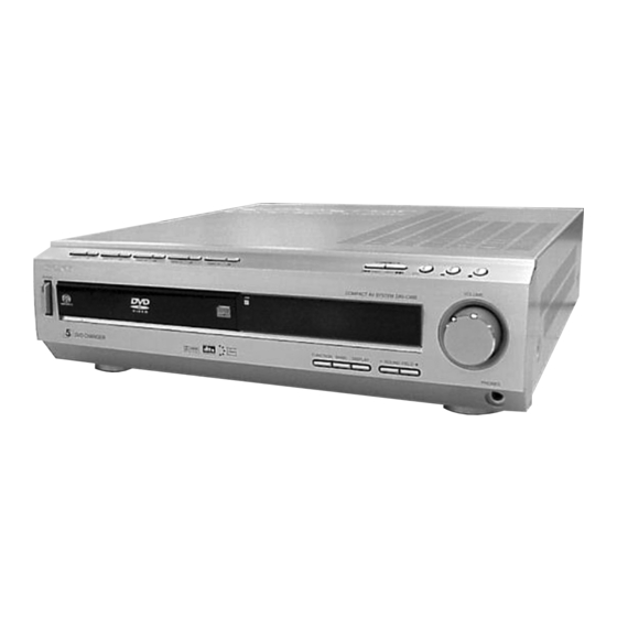
Sony HCD-C450 Service Manual
Compact av system
Hide thumbs
Also See for HCD-C450:
- Operating instructions manual (88 pages) ,
- Service manual (102 pages)
Table of Contents
Advertisement
SERVICE MANUAL
Ver 1.3 2003. 05
HCD-C450 is the amplifier, DVD/CD and tuner
section in DAV-C450.
AUDIO POWER SPECIFICATIONS
POWER OUTPUT AND TOTAL HARMONIC DISTORTION:
With 3 ohms loads, both channels driven, from 120 – 10,000 Hz; rated
80 watts per channel minimum RMS power, with no more than 10 %
total harmonic distortion from 250 milliwatts to rated output.
Amplifier section
Stereo mode
North American and Mexican models:
80 W + 80 W (3 ohms at 1 kHz, THD 10 %)
Other models:
70 W + 70 W (4 ohms at 1 kHz, THD 10 %)
Surround mode
North American and Mexican models:
Front: 80 W + 80 W
Center*: 80 W
Rear*: 80 W + 80 W (3 ohms at 1 kHz, THD 10 %)
Subwoofer*: 100 W (3 ohms at 100 Hz, THD 10 %)
Other models:
Front: 70 W + 70 W
Center*: 70 W
Rear*: 70 W + 70 W (4 ohms at 1 kHz, THD 10 %)
Subwoofer*: 100 W (3 ohms at 100 Hz, THD 10 %)
* Depending on the sound field settings and the source, there may be no sound output.
Inputs (Analog)
AUDIO 1, 2:
Sensitivity: 150 mV
Impedance: 50 kilohms
Inputs (Digital)
AUDIO 2 (optical):
Sensitivity: –
Outputs (Analog)
AUDIO 1 (AUDIO OUT):
Voltage: 2 V
Impedance: 1 kilohms
PHONES:
Accepts low and high-impedance headphones
Super Audio CD/DVD system
Laser
Semiconductor laser
(Super Audio CD/DVD: λ = 650 nm)
(CD: λ = 780 nm)
Emission duration: continuous
Signal format system
NTSC or NTSC/PAL
Frequency response (at 2 CH STEREO mode)
DVD (PCM): 2 Hz to 22 kHz (±1.0 dB)
CD: 2 Hz to 20 kHz (±1.0 dB)
Signal-to-noise ratio
More than 80 dB (AUDIO 1 (AUDIO) connectors only)
Harmonic distortion
Less than 0.03 %
Sony Corporation
9-874-002-04
2003E16-1
Home Audio Company
© 2003.05
Published by Sony Engineering Corporation
HCD-C450
Model Name Using Similar Mechanism
Mechanism Type
Base Unit Name
Optical Pick-up Name
SPECIFICATIONS
FM tuner section
System
North American model:
Other models:
Antenna
Antenna terminals
AM tuner section
System
Tuning range
North American model:
Middle Eastern, and Philipinne models:
Other models:
Antenna
Video section
Outputs
General
Power requirements
North American model:
Australian and Asian models:
Middle Eastern, and Philippine models:
Power consumption
Dimensions (approx.)
Mass (approx.)
Operating temperature
Operating humidity
Design and specifications are subject to change without notice.
US Model
Canadian Model
E Model
Australian Model
NEW
CDM53K-DVBU7
DVBU7
KHM-240AAA
PLL quartz-locked digital synthesizer system
87.5 – 108.0 MHz (100 kHz step)
87.5 – 108.0 MHz (50 kHz step)
FM wire antenna
75 ohms, unbalanced
Tuner section:
PLL quartz-locked digital synthesizer system
530 – 1,710 kHz (with the interval set at 10 kHz)
531 – 1,710 kHz (with the interval set at 9 kHz)
531 – 1,602 kHz (with the interval set at 9 kHz)
531 – 1,602 kHz (with the interval set at 9 kHz)
530 – 1,710 kHz (with the interval set at 10 kHz)
Loop antenna
VIDEO: 1 Vp-p 75 ohms
S-VIDEO: Y: 1 Vp-p 75 ohms
C: 0.286 Vp-p 75 ohms
COMPONENT: Y: 1 Vp-p 75 ohms
P
/C
, P
/C
: 0.7 Vp-p 75 ohms
B
B
R
R
120 V AC, 60 Hz
220 – 240 V AC, 50/60 Hz
110 – 240 V/ 220 – 240 V AC, 50/60 Hz
120 W (120 V AC), 120 W (230 V AC)
355 × 100 × 394 mm (14 × 4 × 15
5
/
inches) (w/h/d) incl. projecting parts
8
5.5 kg (12 lb 3 oz)
5˚C to 35˚C (41˚F to 95˚F)
5 % to 90 %
COMPACT AV SYSTEM
Advertisement
Table of Contents

Related Manuals for Sony HCD-C450


Summary of Contents for Sony HCD-C450
-
Page 1: Specifications
HCD-C450 SERVICE MANUAL US Model Canadian Model Ver 1.3 2003. 05 E Model Australian Model HCD-C450 is the amplifier, DVD/CD and tuner section in DAV-C450. Model Name Using Similar Mechanism Mechanism Type CDM53K-DVBU7 Base Unit Name DVBU7 Optical Pick-up Name... - Page 2 To prevent a malfunction, the front panel display. Refer to the following (xx is a number) system has performed the self- table. diagnosis function. , Contact your nearest Sony dealer or local authorized C:13:00 Sony service facility and give the 5-character service number.
- Page 3 HCD-C450 Ver 1.3 2003. 05 SAFETY CHECK-OUT Laser component in this product is capable of emitting radiation exceeding the limit for Class 1. After correcting the original service problem, perform the following safety checks before releasing the set to the customer: Check the antenna terminals, metal trim, “metallized”...
-
Page 4: Table Of Contents
CRITIQUES POUR LA SÉCURITÉ DE FONCTIONNEMENT. NE COMPONENTS WITH SONY PARTS WHOSE PART NUMBERS REMPLACER CES COMPOSANTS QUE PAR DES PIÈSES SONY APPEAR AS SHOWN IN THIS MANUAL OR IN SUPPLEMENTS DONT LES NUMÉROS SONT DONNÉS DANS CE MANUEL OU PUBLISHED BY SONY. -
Page 5: General
HCD-C450 SECTION 1 This section is extracted GENERAL from instruction manual. Index to Parts and Controls For more information, refer to the pages indicated in parentheses. Front Panel 1 POWER switch/indicator (32) 8 PHONES jack (32) 2 DISC 1 (play) / A (open/close)-DISC 5... - Page 6 HCD-C450 1 TV [/1 (on/standby) (62) Remote 2 Z OPEN/CLOSE (32) 3 NAME (65) 4 STEREO/MONO (64) 5 MEMORY (30) 6 CLEAR (39) 7 PLAY MODE (39) 8 AUDIO (47) 9 ANGLE (54) q; SUBTITLE (55) qa VOL +/– (62) qs ./>, PREV/NEXT, TV CH +/–,...
-
Page 7: Disassembly
HCD-C450 SECTION 2 DISASSEMBLY • The equipment can be removed using the following procedure. CASE (TOP) TUNER UNIT FRONT PANEL SECTION POWER BOARD MECHANISM DECK (CDM53K-DVBU7) RF-240 BOARD OPTICAL PICK UP (KHM-240AAA) FITTING BASE (MAGNET) ASSEMBLY DVD BASE UNIT (DVBU7) -
Page 8: Tuner Unit
HCD-C450 2-2. Tuner Unit 4 flexible flat cable (13core) 7 tuner unit 1 screw, +BVTP (3 × 8) 5 earth wire 6 two screws, +BVTP (3 × 8) 2 screw, +BVTP (3 × 8) 3 chassis 2-3. Front Panel Section... -
Page 9: Power Board
HCD-C450 2-4. POWER Board 5 two screws, +BVTP 6 wire (3 × 8) 7 two screws, +BVTP (3 × 8) 9 POWER board 2 connector (CN901) 8 hook 3 connector (CN902) 1 connector (CN905) 4 connector (CN904) 2-5. Mechanism Deck (CDM53K-DVBU7) -
Page 10: Board
HCD-C450 2-6. RF-240 Board 1 three screws +BVTP (2.6 × 8) 3 flexible flat cable (9 core) 4 RF-240 board (CN003) 2 flexible flat cable (26 core) (CN001) 2-7. Fitting Base (Magnet) Assembly 2 four screws +BVTP (2.6 × 8) -
Page 11: Dvd Base Unit (Dvbu7)
HCD-C450 2-8. DVD Base Unit (DVBU7) 1 two floating screws, + PTPWHM (2.6 × 6) 2 DVD base unit (DVBU7) 2-9. Optical Pick-up (KHM-240AAA) 1 step screw (L) 2 two step screws (S) 7 three insulators 8 optical pick-up (KHM-240AAA) -
Page 12: Clamp Motor Board
HCD-C450 2-10. CLAMP MOTOR Board, Motor (Clamp) Assembly 1 belt (mode) 5 motor (clamp) assembly (M701) 4 CLAMP MOTOR board 3 Remove the two solderings. 2 two screws +BVTP (2.6 × 8) 2-11. Fitting Base (Guide) Assembly, Bracket (Chassis) 2 four screws... -
Page 13: Tray (240)
HCD-C450 2-12. Tray (240) 1 Rotating the pulley (LD)-A , shift the slider (selection) in the arrow A direction. 2 Rotating the pulley (LD)-B in the arrow direction, adjust the tray (240) to be removed. 3 Rotating the pulley (LD)-A , shift the slider (selection) in the arrow B direction. -
Page 14: Load Motor Board, Motor (Loading) Assembly (M702)
HCD-C450 2-14. LOAD MOTOR Board, Motor (Loading) Assembly (M702) 1 belt (communication) 2 belt (loading) 3 belt (loading) 7 motor (loading) assembly (M702) 6 LOAD MOTOR board 5 Remove the two solderings. 4 two screws +BVTP (2.6 × 8) 2-15. Stocker Section... -
Page 15: Slider (Selection), Tension Spring (Shutter)
HCD-C450 2-16. Slider (Selection), Tension Spring (Shutter), Slider (Shutter) 1 two floating screws PRECAUTION DURING SLIDER +PTPWHM, (SELECTION) INSTALLATION (2) (2.6 x 6) 4 slider (selection), Insert the slider (selection) 2 washer, 8 tension spring (shutter), slider (shutter) into the portion A. -
Page 16: Gear (Gear A), Gear (Gear B), Gear (U/D Slider)
HCD-C450 2-17. Gear (Gear A), Gear (Gear B), Gear (U/D Slider) 5 gear (gear A) 6 gear (gear B) 7 screw +BVTP (2.6 × 8) 2 washer 3 compression spring 8 gear (U/D slider) 4 gear (selection) 1 gear (relay) -
Page 17: Gear (Chucking)
HCD-C450 2-18. Gear (Chucking) PRECAUTION DURING GEAR (CHUCKING) (2) rotary encoder gear 3 gear (chucking) (chucking) (S707) rotary encoder (S707) Align with the slot of rotary encoder. PRECAUTION DURING GEAR (CHUCKING) (1) rotary encoder (S707) Align marking. -
Page 18: Test Mode
HCD-C450 Ver 1.3 2003. 05 SECTION 3 TEST MODE Version Display Mode OSD Test Mode Procedure: Procedure: Press the A button on the main unit or ?/1 button on the Press the A button on the main unit or ?/1 button on the remote commander to turn the set on. - Page 19 HCD-C450 Syscon Diagnosis [PREV] Press x key to quit the diagnosis, or key to repeat the The same contents as board detail check by serial interface can be [NEXT] same item where an error occurred, or key to continue the checked from the remote commander.
- Page 20 HCD-C450 3. Peripheral (5-3) ARP to RAM Data Bus Data write → read, and accord check Error 09: ARP ←→ RAM data bus error (3-2) EEPROM Check Data write → read, and accord check Data 0x0001 to 0x8000 where one bit each is set to 1 are...
- Page 21 HCD-C450 6. AV Decoder Check Items List (6-2) 1930 RAM 2) Version Data write → read, and accord check (2-2) Revision Error 13: AVD RAM read data discord (2-3) ROM Check Sum The program code data stored in ROM (IC107 or IC108) (2-4) Model Type are copied to all areas oo»RAM (IC504, IC505) connected...
- Page 22 HCD-C450 Ver 1.3 2003. 05 Drive Auto Adjustment 1. DVD-SL (single layer) [ENTER] Select , insert DVD single layer disc, and press key, On the Test Mode Menu screen, press key on the remote and the adjustment will be made through the following steps, then commander, and the drive auto adjustment menu will be displayed.
- Page 23 HCD-C450 2. CD 3. DVD-DL (dual layer) [ENTER] [ENTER] Select , insert CD disc, and press key, and the Select , insert DVD dual layer disc, and press key, and adjustment will be made through the following steps, then adjusted the adjustment will be made through the following steps, then values will be written to the EEPROM.
- Page 24 HCD-C450 4. LCD Drive Manual Operation [ENTER] Select , insert SACD disc, and press key, and the On the Test Mode Menu screen, select , and the manual operation adjustment will be made through the following steps, then adjusted menu will be displayed. For the manual operation, each servo on/ values will be written to the EEPROM.
- Page 25 HCD-C450 0. Disc Check Memory Disc Type 1. Disc Type Auto Check Disc Check 2. DVD SL 12 cm 3. DVD DL 12 cm 4. CD 12cm 5. LCD 12 cm 1. SL Disc Check 6. DVD SL 8 cm 2.
- Page 26 HCD-C450 Reset SLED TILT Reset the Sled and Tilt to initial position. 6. Memory Check Turn ON/OFF the laser. EEPROM Data1 -– DL –- CD LCD Turn ON/OFF the spindle. Focus Gain xx xx TRK. Gain xx xx Focus Search the focus and turn on the focus.
- Page 27 HCD-C450 Emergency History 34: Focus gain adjustment error 35: Tilt servo adjustment error 36: RF equalizer adjustment error ### EMG. History ### 37: RF group delay adjustment error Laser Hours xxxxxxxh 38: Jitter value after adaptive servo operation is too large.
-
Page 28: Electrical Adjustment
HCD-C450 SECTION 4 ELECTRICAL ADJUSTMENT Adjustment Of Video System In making adjustment, refer to Adjustment Re- lated Parts Arrangement. 1. Video Level Adjustment (DVD BOARD) <Purpose> Note: During diagnostic check, the characters and color bars can This adjustment is made to satisfy the NTSC standard, and if not be seen only with the NTSC monitor. - Page 29 HCD-C450 3. Checking S Video Output S-C (DVD BOARD) Adjustment Related Parts Arrangement <Purpose> DVD BOARD (SIDE A) This checks whether the S-C satisfies the NTSC Standard. If it is not correct, the colors will be too dark or light.
-
Page 30: Diagrams
HCD-C450 SECTION 5 DIAGRAMS • Circuit Boards Location IN SW board CONNECTOR board SW 1179 board COMPONENT board I/O board DS 1179 board DDCON 1179 board Tuner UNIT DVD board FU 1179 board HP 1179 board CLAMP MOTOR board RF-240 board... - Page 31 HCD-C450 • Waveforms THIS NOTE IS COMMON FOR PRINTED WIRING – RF-240 Board – – DVD Board – – AMP Board – – COMPONENT Board – BOARDS AND SCHEMATIC DIAGRAMS. (In addition to this, the necessary note is printed in each block.) 1.5 Vp-p...
-
Page 32: Block Diagrams
HCD-C450 5-1. Block Diagrams – RF/Servo, Video Section – OPTICAL PICK-UP (KHM-240 AAA) IC503 IC001 AV DECODER DVD/CD RF AMP IC302 SERVO DSP DIGITAL SERVO RF IN RFIN1 HD8-15 DVD/CD SIGO D0-7 IC701 HD0-15 PDIC VIDEO AMP RFIN2 ADC0 COMP OUT... - Page 33 HCD-C450 – CPU Section – IC600 INPUT SEL J600 (1/2) IC603 AUDIO 1 IC606 DIGITAL AUDIO AUDIO 2 10 9 IC602 I/F RECEIVER OPTICAL AUDIO 2 DIGITAL DIN1 Q603 Q604 IC602 AUDIO RF/SERVO SPDIF DIN0 A/D CONV SECTION ASEL2 DOUT...
- Page 34 HCD-C450 – Power Section – IC305 IC301 J401 (1/2) STREAM PROCESSOR POWER DRIVER (F) L401,C451 DATA OUTL1+ OUTA FRONT OUTL2+ L401,C452 OUTB OUTR1+ R-CH L402,C453 OUTR2+ R-CH DIAG AUDIO-1 XFS1 REAR BCKO L402,C454 SECTION LRCKO LRCK RY301 SCDT +27V SCSHIFT...
-
Page 35: Printed Wiring Board - Rf Board
HCD-C450 5-2. Printed Wiring Board – RF Board – • See page 30 for Circuit Boards Location. CN009 IC001 • Semiconductor Location Ref. No. Location D001 D004 IC001 Q001 Q002... -
Page 36: Schematic Diagram - Rf Board
HCD-C450 5-3. Schematic Diagram – RF Board – • See page 31 for Wavefoms. • See page 65 for IC Block Diagrams. 6.3V IC B/D SPM+ SPM+ SPM- SPM- INLIM INLIM SLA- SLA- SLB- SLB- C N 0 0 3... -
Page 37: Printed Wiring Board - Dvd Board (Side A)
HCD-C450 5-4. Printed Wiring Board – DVD Board (Side A) – • See page 30 for Circuit Boards Location. IC302 EXCEPT US,CND EXCEPT US,CND IC106 IC503 N.C. IC103 IC903 • Semiconductor IC612 Location IC801 Ref. No. Location IC607 D901 D903... -
Page 38: Printed Wiring Board - Dvd Board (Side B)
HCD-C450 5-5. Printed Wiring Board – DVD Board (Side B) – • See page 30 for Circuit Boards Location. IC001 IC003 IC006 IC401 IC504 IC304 IC303 IC505 IC108 • Semiconductor IC102 Location Ref. No. Location D900 D902 IC001 IC003 IC006... -
Page 39: Schematic Diagram - Dvd Board (1/9)
HCD-C450 5-6. Schematic Diagram – DVD Board (1/9) – • See page 31 for Wavefoms. • See page 63 for IC Block Diagrams. (3/9) (4/9) (2/9) IC B/D (2/9) (5/9) R026 R028 R029 R031 R032 (1/2) R034 (2/9) (4/9) -
Page 40: Schematic Diagram - Dvd Board (2/9)
HCD-C450 5-7. Schematic Diagram – DVD Board (2/9) – • See page 31 for Wavefoms. • See page 63 for IC Block Diagrams. (4/9) (1/9) (4/9) (1/9) IC B/D (4/9) R656 R617 (1/9) DTA124EKA-T146 (8/9) uPC2926T-1-E1 DTA124EKA-T146 DTA124EKA-T146 (8/9) (4/9) -
Page 41: Schematic Diagram - Dvd Board (3/9)
HCD-C450 5-8. Schematic Diagram – DVD Board (3/9) – 6/9, 8/9, 9/9 8/9,9/9 6/9, 8/9 5/9,6/9,8/9,9/9 R532 6/9,8/9,9/9 6/9,8/9 6/9,8/9,9/9 6/9, 8/9 R508 R509 5/9, 6/9 5/9,6/9 4/9, 6/9 5/9,6/9,8/9... -
Page 42: Schematic Diagram - Dvd Board (4/9)
HCD-C450 5-9. Schematic Diagram – DVD Board (4/9) – 6 / 9 6 / 9 R024 6 / 9 , 7 / 9 R022 R002 R003 7 / 9 R004 2 / 9 R005 6 / 9 R006 R007 6 / 9 , 7 / 9... -
Page 43: Schematic Diagram - Dvd Board (5/9)
HCD-C450 5-10. Schematic Diagram – DVD Board (5/9) – • See page 73 for IC Pin Function Descriptions. R801 0 R802 R803 R804 R805 R806 R807 R808 R843 R846 R847 3/9, 6/9 3/9, 6/9 3/9, 6/9, 8/9 3/9, 6/9, 8/9, 9/9... -
Page 44: Schematic Diagram - Dvd Board (6/9)
HCD-C450 5-11. Schematic Diagram – DVD Board (6/9) – • See page 69 for IC Pin Function Descriptions. 3/9,5/9 R329 TO DVD BOARD (4/9,7/9,8/9,9/9) (Page 42) R330 0 (Page 45) (Page 46) R318 0 C352 (Page 47) R332 3/9,4/9 R320 0... -
Page 45: Schematic Diagram - Dvd Board (7/9)
HCD-C450 5-12. Schematic Diagram – DVD Board (7/9) – 8/9,9/9 4/9,6/9 4/9,6/9,8/9,9/9 R439 4/9,6/9 4/9, 9/9... -
Page 46: Schematic Diagram - Dvd Board (8/9)
HCD-C450 5-13. Schematic Diagram – DVD Board (8/9) – • See page 31 for Wavefoms. • See page 63 for IC Block Diagrams. • See page 66 for IC Pin Function Descriptions. 7/9,9/9 FGAINT R154 R150 15k (AUS,E32,MX) 3.3 (AUS) -
Page 47: Schematic Diagram - Dvd Board (9/9)
HCD-C450 5-14. Schematic Diagram – DVD Board (9/9) – 4/9,6/9,... -
Page 48: Printed Wiring Board - Amp Board (Side A)
HCD-C450 5-15. Printed Wiring Board – AMP Board (Side A) – • See page 30 for Circuit Boards Location. IC312 IC310 IC308 IC305 IC303 • Semiconductor Location IC300 Ref. No. Location D330 D331 D332 D333 D334 D335 D340 D341 D342... -
Page 49: Printed Wiring Board - Amp Board (Side B)
HCD-C450 5-16. Printed Wiring Board – AMP Board (Side B) – • See page 30 for Circuit Boards Location. IC311 IC304 IC307 • Semiconductor IC306 Location Ref. No. Location D310 D311 D312 D313 D314 IC309 D315 D320 D321 D322 D323... -
Page 50: Schematic Diagram - Amp Board (1/2)
HCD-C450 5-17. Schematic Diagram – AMP Board (1/2) – • See page 31 for Wavefoms. 220p 220p R338 0 R346 0 R347 0... -
Page 51: Schematic Diagram - Amp Board (2/2)
HCD-C450 5-18. Schematic Diagram – AMP Board (2/2) – TO HP 1179 CNP900 C441 0.01 C442 0.01 TP-HFE R476 FB365 2200 LI136V LI136V LI136V LI136V LI136V LI136V LI136V LI136V LI136V LI136V LI136V LI136V... -
Page 52: Printed Wiring Board - I/O Section
HCD-C450 5-19. Printed Wiring Board – I/O Section – • See page 30 for Circuit Boards Location. (SIDE B) (SIDE A) IC602 IC601 IC702 IC701 IC600 (SIDE A) (SIDE B) IC703 • Semiconductor Location Ref. No. Location Ref. No. Location Ref. No. Location... -
Page 53: Schematic Diagram - I/O Section (1/2)
HCD-C450 5-20. Schematic Diagram – I/O Section (1/2) – • See page 64 for IC Block Diagrams. R606,607 R609,612,618 5.1k(EXCEPT AUS) 10k(EXCEPT AUS) 5.6k(AUS) 33k(AUS) IC B/D SWITCH SWITCH... -
Page 54: Schematic Diagram - I/O Section (2/2)
HCD-C450 5-21. Schematic Diagram – I/O Section (2/2) – • See page 31 for Wavefoms. -
Page 55: Printed Wiring Board - Front Section
HCD-C450 5-22. Printed Wiring Board – FRONT Section – • See page 30 for Circuit Boards Location. IC801 IC802 • Semiconductor Location Ref. No. Location D806 D807 D808 D809 D810 Q803 Q804... -
Page 56: Schematic Diagram - Front Section
HCD-C450 5-23. Schematic Diagram – FRONT Section – • See page 64 for IC Block Diagrams. 1179 1179 1179 EXCEPT US,CND,MX FB806 FB806 US,CND,MX US,CND,MX FB80 7 FB80 7 IC B/D EXCEPT US,CND,MX R839 R845 US,CND,MX EXCEPT US, 1179 C901... -
Page 57: Printed Wiring Board - Sw Section
HCD-C450 5-24. Printed Wiring Board – SW Section – • See page 30 for Circuit Boards Location. IC800... -
Page 58: Schematic Diagram - Sw Section
HCD-C450 5-25. Schematic Diagram – SW Section – 1179 1179 2.2k 1.5k 4.7k 1179 1179 1179... -
Page 59: Printed Wiring Board - Cdm Section
HCD-C450 5-26. Printed Wiring Board – CDM Section – • See page 30 for Circuit Boards Location. DISC IN DETECT SENSOR IC 702 IC 701... -
Page 60: Schematic Diagram - Cdm Section
HCD-C450 5-27. Schematic Diagram – CDM Section – PT483F1 S-TP MTZJ-T-77-3.6B DVD BOARD(9/9) CN201 (Page 47) MTZJ-T-77-5.1B DVD BOARD(9/9) CN202 (Page 47 ) -
Page 61: Printed Wiring Board - Power Board
HCD-C450 Ver 1.2 2002.10 5-28. Printed Wiring Board – POWER Board – • See page 30 for Circuit Boards Location. AUS,E12,E32,SP,EA US,CND,MX,E32 US,CND,MX • Semiconductor Location Ref. No. Location D901 D902 D903 IC906 D904 D905 D906 D907 D908 IC903 D909... -
Page 62: Schematic Diagram - Power Board
HCD-C450 5-29. Schematic Diagram – POWER Board – • See page 64 for IC Block Diagrams. 3.3k 2SB1640 2200 2200 AUS,E12,E32,SP,EA SI-8050JF US,CND,MX 2200 2.2k MTZJ-T-77-24A 11EQS10-TA1 SI-8050JF 100V US,CND,MX,E32 2SD1616A-TP-LK TP-HFE US,CND,MX STR-F6676 MTZJ-T-77-24A 11ES04-TA1B PC901 5.6k IC B/D C901 0.047 (US,CND,MX) -
Page 63: Ic Block Diagrams
HCD-C450 5-30. IC Block Diagrams IC102 SM8707-G-E2 (DVD BOARD) IC606 LC89056W-E (DVD BOARD) AUDIO C BIT PA/PB DETECT DETECT EMPHA SAMPLING FREQUENCY MICROCOMPUTER INTERFACE XSEL LOCK XOUT CLOCK DETECT XMCK 19 DVDD MODE0 MODE 18 DGND SELECT MODE1 XSTATE DGND... - Page 64 HCD-C450 IC802 MSM9202-05GS-KDR1 (FP 1179 BOARD) IC600 MC14052BDR2 (I/O BOARD) Timing Timing Generator 2 Generator 1 64 VDD Duty Control Digit 63 DAT 8bit Control Shift 62 CLK Register 61 CS Port Control Driver Circuit 60 RST Command Decoder Read...
- Page 65 HCD-C450 IC001 SP3728AC (RF-240 BOARD) FULL WAVE CHARGE RECTIFIER PUMP RFIP SDEN PROGRAMABLE EQ FILTER RFIN SCLK BOTTOM LEVEL RF HOLD EN WOBLE BPF TZIN PHASE DETECTOR PHASE DETECTOR VREF SERIAL CONTROL PORT SIGNALS REGISTER BYP2 PEAK/ MIRR BOTTOM HOLD...
-
Page 66: Ic Pin Function Descriptions
HCD-C450 5-31. IC Pin Function Descriptions • IC103 MB91307APFV-G-BND-E1 (SYSTEM CONTROL) (DVD BOARD) Pin No. Pin Name Description 1 to 5 HA17 - 21 Address signal output HA22 Address signal output (Not used) I2C EEPROM write protect signal output TRM/XKRCS... - Page 67 HCD-C450 Pin No. Pin Name Description – Power supply CKSW1 Chucking switch (Tray SW1) signal input OCSW1 Open/Close switch (Tray SW2) signal input CS0X Chip select signal output to external ROM CS1X – Not used CS2X Chip select signal output to AVD SDRAM...
- Page 68 HCD-C450 • IC302 CXD9635R (SERVO DSP) (DVD BOARD) Pin No. Pin Name Description – Digital Ground CPU data VDD 3.3V – Digital power supply 3.3V CPU address – Digital Ground CPU address VDD 1.8V – Digital power supply 1.8V XINT...
- Page 69 HCD-C450 Pin No. Pin Name Description DRAM data – Digital Ground MD10 MD11 DRAM data MD12 MD13 MD14 MD15 VDD 3.3V – Digital power supply 3.3V DATA CDDA data BCLK CDDA bit clock – Digital Ground LRCK CDDA LR clock...
- Page 70 HCD-C450 Pin No. Pin Name Description ADO5 ADO6 ADC output ADO7 – Digital Ground VSSA4 – Analog Ground VCO control input VCO outside resistance 1 VCO outside resistance 2 VDDA4 3.3V – Analog power supply VSSA3 – Analog Ground OP amp positive input...
- Page 71 HCD-C450 Pin No. Pin Name Description VRTA ADC reference – Digital Ground TESTK0 TESTK1 Test terminal L TESTK2 XDSPRST DSP reset XARPRST Reset – Digital Ground MDS0 CLV speed error Motor on MDP0 CLV phase error DFCT Defect detection output...
- Page 72 HCD-C450 Pin No. Pin Name Description VDD 3.3V – Digital power supply 3.3V PDM0 PDM1 PDM output PDM2 PDM3 – Digital Ground CPU light CPU lead...
- Page 73 HCD-C450 • IC801 CXD2752R (PLAYBACK SIGNAL PROCESSOR) (DVD BOARD) Pin No. Pin Name Description VSCA0 – Ground XMSLAT Latch signal input for micom serial communication MSCK Shift clock input for micom serial communication MSDATI Data input for micom serial communication VDCA0 –...
- Page 74 HCD-C450 Pin No. Pin Name Description VDDSD0 – Power supply for DSD data output ZDFC Cch zero data detection flag signal output (open) DSAC Cch DSD data output ZDFLFE LFEch zero data detection flag signal output (open) DSALFE LFEch DSD data output VSDSD1 –...
- Page 75 HCD-C450 Pin No. Pin Name Description VSIOA3 – Ground for I/O (Not used) DCLK Clock output terminal for SDRAM DCKE Clock enable signal output for SDRAM Write enable signal output for SDRAM XCAS Column address strobe signal output for SDRAM...
-
Page 76: Exploded Views
HCD-C450 Ver 1.3 2003.05 SECTION 6 EXPLODED VIEWS NOTE: • -XX, -X mean standardized parts, so they may • Abbreviation The components identified by mark 0 or have some difference from the original one. AUS : Australian model. dotted line with mark 0 are critical for safety. -
Page 77: Chassis Section
HCD-C450 6-2. Chassis Section supplied F901 supplied Overall section supplied (CDM53K -DVBU7) supplied supplied supplied supplied Front panel section Ref. No. Part No. Description Remark Ref. No. Part No. Description Remark A-4726-404-A TUNER UNIT (US, CND) 1-823-083-11 CABLE, FLEXIBLE FLAT (9 CORE) -
Page 78: Front Panel Section
HCD-C450 6-3. Front Panel Section S901 supplied supplied supplied Supplied with S800 Ref. No. Part No. Description Remark Ref. No. Part No. Description Remark 4-234-934-21 PANEL (AL), FRONT A-4676-753-A FP 1179 BOARD, COMPLETE X-4954-752-2 WINDOW SUB ASSY (FL) 1-681-999-13 FU 1179 BOARD... -
Page 79: Overall Section (Cdm53K-Dvbu7)
HCD-C450 6-4. Overall Section (CDM53K-DVBU7) not supplied Chassis (mold) assembly section (CDM53K-DVBU7) not supplied Chassis section (CDM53K-DVBU7) Ref. No. Part No. Description Remark Ref. No. Part No. Description Remark 3-341-549-01 SCREW(2.6X12)(DIA.7.5),+PTP WH A-4672-872-A BASE (MAGNET) ASSY, FITTING 4-951-620-41 SCREW (2.6), +BVTP... - Page 80 HCD-C450 6-5. Chassis (Mold) Assembly Section (CDM53K-DVBU7) supplied M702 Ref. No. Part No. Description Remark Ref. No. Part No. Description Remark 4-951-620-41 SCREW (2.6), +BVTP 4-211-228-01 LEVER (GOOSENECK) 4-211-235-01 BELT (COMMUNICATION) 4-214-130-01 GEAR (TRAY) 4-211-236-01 BELT (LOADING) 4-211-209-12 CHASSIS (MOLD B)
-
Page 81: Chassis Section (Cdm53K-Dvbu7)
HCD-C450 6-6. Chassis Section (CDM53K-DVBU7) supplied Stocker (240) overall section S707 supplied Optical pick-up section M701 (DVBU7) Ref. No. Part No. Description Remark Ref. No. Part No. Description Remark 4-951-620-41 SCREW (2.6), +BVTP 4-211-217-02 GEAR (SELECTION) 4-230-548-11 SCREW (J), STEP... -
Page 82: Optical Pick-Up Section (Dvbu7)
HCD-C450 6-7. Stocker (240) Overall Section, Optical Pick-up Section (DVBU7) not supplied Ref. No. Part No. Description Remark Ref. No. Part No. Description Remark A-4726-883-A RF-240 MOUNTED BOARD, COMPLETE 4-236-579-01 SCREW (S), STEP X-4954-130-2 HOLDER (240) ASSY 4-234-047-01 TRAY (240) -
Page 83: Electrical Parts List
HCD-C450 SECTION 7 ELECTRICAL PARTS LIST Note: • Due to standardization, replacements in the • RESISTORS • CAPACITORS uF : µ F parts list may be different from the parts All resistors are in ohms specified in the diagrams or the components METAL: Metal-film resistor •... - Page 84 HCD-C450 Ref. No. Part No. Description Remarks Ref. No. Part No. Description Remarks C402 1-163-021-91 CERAMIC CHIP 0.01uF 10.00% 50V D324 8-719-073-82 DIODE SFPB-76V C403 1-126-948-11 ELECT 100uF 20.00% 35V D325 8-719-073-82 DIODE SFPB-76V C404 1-107-826-11 CERAMIC CHIP 0.1uF 10.00% 16V...
- Page 85 HCD-C450 CLAMP MOTOR COMPONENT Ref. No. Part No. Description Remarks Ref. No. Part No. Description Remarks IC310 6-700-279-01 IC CXD9634AQ R348 1-216-809-11 METAL CHIP 1/16W IC311 6-701-741-01 IC CXD9646A R349 1-216-809-11 METAL CHIP 1/16W IC312 8-759-834-30 IC MC74VHC1G08DFT1 R350 1-216-809-11 METAL CHIP 1/16W <...
- Page 86 HCD-C450 COMPONENT CONNECTOR DDCON 1179 DS 1179 Ref. No. Part No. Description Remarks Ref. No. Part No. Description Remarks < IC > < RESISTOR > IC703 8-759-522-11 IC BA7660FS-E2 R850 1-216-828-11 METAL CHIP 3.9K 1/16W R855 1-216-809-11 METAL CHIP 1/16W <...
- Page 87 HCD-C450 Ref. No. Part No. Description Remarks Ref. No. Part No. Description Remarks A-4676-740-A DVD BOARD, COMPLETE (US,CND) C317 1-164-947-11 CERAMIC CHIP 0.01uF A-4729-816-A DVD BOARD, COMPLETE (E12) A-4729-827-A DVD BOARD, COMPLETE (AUS) C318 1-164-947-11 CERAMIC CHIP 0.01uF A-4729-832-A DVD BOARD, COMPLETE (EA)
- Page 88 HCD-C450 Ref. No. Part No. Description Remarks Ref. No. Part No. Description Remarks C506 1-117-370-11 CERAMIC CHIP 10uF C623 1-164-850-11 CERAMIC CHIP 10PF 0.50PF 50V C508 1-164-947-11 CERAMIC CHIP 0.01uF C509 1-164-947-11 CERAMIC CHIP 0.01uF C624 1-107-820-11 CERAMIC CHIP 0.1uF...
- Page 89 HCD-C450 Ref. No. Part No. Description Remarks Ref. No. Part No. Description Remarks C802 1-164-947-11 CERAMIC CHIP 0.01uF < DIODE > C804 1-164-947-11 CERAMIC CHIP 0.01uF C808 1-164-947-11 CERAMIC CHIP 0.01uF D900 8-719-053-18 DIODE 1SR154-400TE-25 C812 1-126-209-11 ELECT CHIP 100uF 20.00% 4V...
- Page 90 HCD-C450 Ref. No. Part No. Description Remarks Ref. No. Part No. Description Remarks IC103 8-759-829-75 IC MB91307APFV-G-BND-E1 < RESISTOR > IC106 6-700-785-01 IC SN74AHCT32PWR R001 1-218-990-11 SHORT IC108 6-801-962-01 IC MR27V3202F-6ATPZ020 R002 1-218-990-11 SHORT IC201 6-700-740-01 IC LC22004A-RJ6-TBM-E R003 1-218-990-11 SHORT...
- Page 91 HCD-C450 Ref. No. Part No. Description Remarks Ref. No. Part No. Description Remarks R058 1-218-990-11 SHORT R154 1-218-967-11 RES-CHIP 1/16W R063 1-218-990-11 SHORT (AUS,E32,MX) R065 1-218-990-11 SHORT R068 1-218-990-11 SHORT R154 1-218-975-11 RES-CHIP 1/16W (EA) R069 1-218-990-11 SHORT R154 1-218-971-11 RES-CHIP...
- Page 92 HCD-C450 Ref. No. Part No. Description Remarks Ref. No. Part No. Description Remarks R309 1-218-961-11 RES-CHIP 4.7K 1/16W R423 1-208-719-11 METAL CHIP 0.5% 1/16W R310 1-218-961-11 RES-CHIP 4.7K 1/16W R424 1-208-719-11 METAL CHIP 0.5% 1/16W R425 1-208-943-11 METAL CHIP 220K 0.5%...
- Page 93 HCD-C450 Ref. No. Part No. Description Remarks Ref. No. Part No. Description Remarks R625 1-218-953-11 RES-CHIP 1/16W R696 1-218-945-11 RES-CHIP 1/16W R626 1-218-953-11 RES-CHIP 1/16W R699 1-218-941-81 RES-CHIP 1/16W R700 1-218-965-11 RES-CHIP 1/16W R627 1-218-957-11 RES-CHIP 2.2K 1/16W R701 1-218-953-11 RES-CHIP...
- Page 94 HCD-C450 FP 1179 Ref. No. Part No. Description Remarks Ref. No. Part No. Description Remarks R914 1-218-941-81 RES-CHIP 1/16W R982 1-218-965-11 RES-CHIP 1/16W R915 1-218-941-81 RES-CHIP 1/16W R983 1-218-965-11 RES-CHIP 1/16W R984 1-218-965-11 RES-CHIP 1/16W R916 1-218-941-81 RES-CHIP 1/16W R985...
- Page 95 HCD-C450 FP 1179 FU 1179 HP 1179 Ref. No. Part No. Description Remarks Ref. No. Part No. Description Remarks FB807 1-469-324-21 FERRITE 0UH (US,CND,MX) R873 1-216-813-11 METAL CHIP 1/16W FB807 1-216-864-11 METAL CHIP 1/16W (EXCEPT US,CND,MX) < ROTARY ENCODER/SWITCH >...
- Page 96 HCD-C450 Ref. No. Part No. Description Remarks Ref. No. Part No. Description Remarks A-4676-746-A I/O BOARD, COMPLETE (US,CND) C735 1-164-156-11 CERAMIC CHIP 0.1uF A-4729-822-A I/O BOARD, COMPLETE (E12,SP,EA) C737 1-124-261-00 ELECT 10uF A-4729-830-A I/O BOARD, COMPLETE (AUS) C738 1-164-156-11 CERAMIC CHIP 0.1uF...
- Page 97 HCD-C450 IN SW Ref. No. Part No. Description Remarks Ref. No. Part No. Description Remarks L702 1-469-525-91 INDUCTOR 10uH R618 1-216-839-11 METAL CHIP 1/16W L703 1-412-953-11 INDUCTOR 15uH (AUS) L705 1-412-953-11 INDUCTOR 15uH L707 1-469-525-91 INDUCTOR 10uH R619 1-216-821-11 METAL CHIP...
- Page 98 HCD-C450 IN SW INIT/COUNT SW LOAD MOTOR OUT SW POWER Ref. No. Part No. Description Remarks Ref. No. Part No. Description Remarks < SWITCH > 0 C901 1-117-699-11 CERAMIC 0.001uF 250V (E32) S703 1-771-218-11 SWITCH, MICRO (MID IN) 0 C902 1-165-528-11 MYLAR 0.1uF...
- Page 99 HCD-C450 Ver 1.2 2002.10 POWER Ref. No. Part No. Description Remarks Ref. No. Part No. Description Remarks C926 1-115-339-11 CERAMIC CHIP 0.1uF 10.00% 50V L902 1-419-253-11 INDUCTOR 100uH C927 1-115-339-11 CERAMIC CHIP 0.1uF 10.00% 50V L903 1-419-253-11 INDUCTOR 100uH C928...
- Page 100 HCD-C450 POWER PW 1179 RF-240 Ref. No. Part No. Description Remarks Ref. No. Part No. Description Remarks 0 R909 1-260-132-11 CARBON 560K 1/2W C006 1-162-966-11 CERAMIC CHIP 0.0022uF 10% (EXCEPT US,CND,MX) C007 1-162-966-11 CERAMIC CHIP 0.0022uF 10% 0 R910 1-215-884-31 METAL OXIDE...
- Page 101 HCD-C450 Ver 1.3 2003.05 RF-240 SENSOR SENSOR 2 SW 1179 Ref. No. Part No. Description Remarks Ref. No. Part No. Description Remarks < RESISTOR > S805 1-786-220-11 SWITCH, KEY BOARD (PRESET –/. PREV) ************************************************************** R002 1-216-809-11 METAL CHIP 1/16W R003...
- Page 102 HCD-C450 REVISION HISTORY Clicking the version allows you to jump to the revised page. Also, clicking the version at the upper right on the revised page allows you to jump to the next revised page. Ver. Date Description of Revision 2002.05...