Yamaha Stagepas 300 Service Manual
Hide thumbs
Also See for Stagepas 300:
- Service manual (55 pages) ,
- Owner's manual (2 pages) ,
- Owner's manual (112 pages)
Advertisement
STAGEPAS 300
SERVICE MANUAL
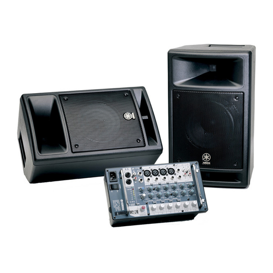
Speaker
Mixer
Speaker
CONTENTS(目次)
SPECIFICATIONS(総合仕様) ............................................... 3
PANEL LAYOUT(パネルレイアウト) .................................. 4
DIMENSIONS(寸法図) ......................................................... 4
CIRCUIT BOARD LAYOUT(ユニットレイアウト) .............. 5
DISASSEMBLY PROCEDURE(分解手順) ........................... 6
IC BLOCK DIAGRAM(ICブロック図) ................................. 15
CIRCUIT BOARDS(シート基板図) ..................................... 16
INSPECTIONS(検査) ......................................................... 23
TROUBLE SHOOTING(トラブルシューティング) ............ 26
BLOCK DIAGRAM(ブロックダイアグラム)
CIRCUIT DIAGRAM(回路図)
PA
011775
20050321-86100
HAMAMATSU, JAPAN
1
Copyright (c) Yamaha Corporation. All rights reserved. PDF-K9611
'05.04
Advertisement
Table of Contents

Related Manuals for Yamaha Stagepas 300


Summary of Contents for Yamaha Stagepas 300
-
Page 1: Table Of Contents
CIRCUIT BOARD LAYOUT(ユニットレイアウト) ....5 DISASSEMBLY PROCEDURE(分解手順) ......6 IC BLOCK DIAGRAM(ICブロック図) ......... 15 CIRCUIT BOARDS(シート基板図) ........16 INSPECTIONS(検査) ............23 TROUBLE SHOOTING(トラブルシューティング) .... 26 PARTS LIST BLOCK DIAGRAM(ブロックダイアグラム) CIRCUIT DIAGRAM(回路図) 011775 20050321-86100 HAMAMATSU, JAPAN Copyright (c) Yamaha Corporation. All rights reserved. PDF-K9611 ’05.04... - Page 2 IMPORTANT NOTICE This manual has been provided for the use of authorized Yamaha Retailers and their service personnel. It has been assumed that basic service procedures inherent to the industry, and more specifically Yamaha Products, are already known and understood by the users, and have therefore not been restated.
-
Page 3: Specifications
STAGEPAS 300 総合仕様 SPECIFICATIONS 一般仕様 General Specifications 最大出力 Maximum Output Power 150 W+150 W/6 Ω @10 % THD at 1 kHz (SPEAKER L/R) ≧150 W+150 W/6 Ω @10 % THD at 1 kHz (SPEAKER L/R) 100 W+100 W/6 Ω @1 % THD at 1 kHz (SPEAKER L/R) ≧100 W+100 W/6 Ω... -
Page 4: Panel Layout(パネルレイアウト
STAGEPAS 300 PANEL LAYOUT(パネルレイアウト) q [POWER] switch ([POWER]スイッチ) w [AC IN] jack ([AC IN]端子) e [SPEAKER L/R] jacks ([SPEAKER L/R]端子(付属のスピーカー用)) r [REC OUT L/R] jacks ([REC OUT L/R]端子) t [MONITOR OUT L(MONO)/R] jacks ([MONITOR OUT L(MONO)/R]端子) y Channel input jacks (CH 1 to 4) (チャンネル入力端子... -
Page 5: Circuit Board Layout(ユニットレイアウト
STAGEPAS 300 CIRCUIT BOARD LAYOUT(ユニットレイアウト)... -
Page 6: Disassembly Procedure
STAGEPAS 300 (分解手順) DISASSEMBLY PROCEDURE フロントグリル Ass'y Front Grille Assembly (所要時間:約 1 分) (Time required: About 1 minute) [120A]のネジ 4 本を外して、フロントグリル Ass'y Remove the four (4) screws marked [120A]. The を外します。 (図 1) front grille assembly can then be removed. (Fig.1) スピーカ... - Page 7 STAGEPAS 300 Speaker HF (Tweeter) Speaker LF (Woofer) (スピーカHF(ツィーター)) (スピーカLF(ウーファー)) Wire LF (Red) Wire LF (Black) Wire HF (Blue) Wire HF (Yellow) (束線LF(赤)) (束線LF(黒)) (束線HF(青)) (束線HF(黄)) Photo 1 ( 写真 1) Photo 2 ( 写真 2) Speaker HF (Tweeter) スピーカHF (ツィーター)...
- Page 8 STAGEPAS 300 ミキサー Ass'y、カバーモールド Ass'y Mixer Assembly, Cover Mold Assembly (所要時間:約 1 分) (Time required: About 1 minute) Rotate the two (2) straight slots on the fastener コインドライバーまたはマイナスドライバーで、 heads with a coin driver or minus driver until each ファスナーヘッドのマイナス形溝 2 箇所を OPEN straight slot is in alignment with the OPEN position.
- Page 9 STAGEPAS 300 ミキサーAss'y (パネル側、 リアケース側) Mixer Assembly (Panel Assembly, Rear Case Assembly) (所要時間:約 3 分) (Time required: About 3 minutes) ミキサー Ass'y を外します。 (6 項参照) Remove the mixer assembly. (See procedure 6) [340]のネジ 8 本を外して、 ミキサーAss'y からパネ Remove the eight (8) screws marked [340], and ル側とリアケース側を別けます。...
- Page 10 STAGEPAS 300 VR シート VR Circuit Board (所要時間:約 10 分) (Time required: About 10 minutes) 10-1 INPUT シートを外します。 (9 項参照) 10-1 Remove the INPUT circuit board. (See procedure 9) 10-2 パネル印刷面から[130]のノブ VR(白)6 個、 [140] 10-2 Remove the six (6) volume knobs (white) marked のノブ...
- Page 11 STAGEPAS 300 [120B] Volume knob (S) (Blue) [100B] Volume knob (S) (White) (ノブVR(S)(青)) (ノブVR(S)(白)) [110A] Volume knob (S) (Green) X 12 (ノブVR(S)(緑)) [90] Push button X 5 (プッシュボタン) Fig.11 ( 図 11) FILTER Circuit Board FILTER シート (所要時間:約 4 分)...
- Page 12 STAGEPAS 300 Panel (パネル) Earth wire (green) (brown) (アース線 (緑)) (茶) Connector assembly (2P) (blue) (束線 2P) (青) Power switch Connector assembly (1P) (brown) (電源スイッチ) (束線 1P (茶)) AC inlet (ACインレット) Soldering (半田付け) Fig.14 ( 図 14) Panel (パネル) Panel (パネル) Claw (ツメ)
- Page 13 STAGEPAS 300 [260] X 7 [270A] POWER [270B] Power amplifier unit B (パワーアンプユニットB) Power amplifier unit A (パワーアンプユニットA) [CN5] [CN6] [CN4] [CN7] Rear case assembly (リアケースAss'y、リアケース側) [260]: Bind Head Tapping Screw-B ( +バインド B タイト ) 3.0X8 CR3 (AAX61980) [270]: Bind Head Tapping Screw-B (+バインドBタイト) 3.0X10 NI-BL (AAX61710) Fig.17 ( 図...
- Page 14 STAGEPAS 300 ファン(小) Fan (Small) (所要時間:約 7 分) (Time required: About 7 minutes) 15-1 Remove the POWER circuit board. 15-1 POWER シートを外します。 (14 項参照) (See procedure 14) 15-2 ファン(小)と共にシールドケースを外します。 15-2 Remove the shield case together with the fan (図 20)...
-
Page 15: Ic Block Diagram
STAGEPAS 300 (ICブロック図) IC BLOCK DIAGRAM M65850FP (AAX62760) Digital Echo FILTER: IC602 CLOCK OP2 IN OP2 OUT LPF2 IN LPF2 OUT LPF2 OSCILLATOR D / A LPF1 IN 1/2 Vcc LPF1 OUT CLOCK CLOCK OP1 OUT AUTO MAIN CONTROL RESET... -
Page 16: Circuit Boards
STAGEPAS 300 (シート基板図) CIRCUIT BOARDS FILTER Circuit Board (6469-40) ............... 22 INPUT Circuit Board (6469-40) ..............16 JACK1A Circuit Board (8143-40) ............. 22 JACK1B Circuit Board (8143-40) ............. 22 JACK2 Circuit Board (6469-40) ..............22 NETWORK1 Circuit Board (8143-40) ............17 NETWORK2 Circuit Board (8143-40) ............ - Page 17 STAGEPAS 300 NETWORK1 Circuit Board Component side(部品側) Pattern side(パターン側) 407751, 407752 407750 NETWORK2 Circuit Board Component side Component side(部品側) Pattern side(パターン側) 407751, 407752 407750...
- Page 18 STAGEPAS 300 POWER Circuit Board Component side(部品側) 407751, 407752...
- Page 19 STAGEPAS 300 POWER Circuit Board Pattern side(パターン側) 407750...
- Page 20 STAGEPAS 300 VR Circuit Board Component side(部品側) 407747...
- Page 21 STAGEPAS 300 VR Circuit Board Pattern side(パターン側) 407744...
- Page 22 STAGEPAS 300 FILTER Circuit Board Component side(部品側) Pattern side(パターン側) 407747 407744 JACK1A Circuit Board JACK1B Circuit Board JACK2 Circuit Board to NETWORK1-CN10 to NETWORK2-CN8 NETWORK1-CN10 NETWORK2-CN8 Component side(部品側) Component side(部品側) Component side(部品側) 407747 407751, 407752 407751, 407752 to POWER-CN9 Pattern side(パターン側)...
-
Page 23: Inspections(検査
STAGEPAS 300 (検査) INSPECTIONS Test Conditions(試験条件) Measuring Voitage(測定電圧): AC 100 V 50/60 Hz (J) AC 120 V 60 Hz (U, C, V) AC 240 V 50 Hz (A) AC 230 V 50 Hz (B, H, W) AC 220 V 60 Hz (K) AC 220 V 50 Hz (O) 6 Ω... - Page 24 STAGEPAS 300 ITEM INPUT CONDITIONS OUTPUT CONDITIONS NOMINAL LIMIT (項目) (入力条件) (出力条件) (標準値) (限界値) INPUT SENSITIVITY INPUT 1, 2, 3, 4 (Each) SP OUT: L, R -23 dBu -23 dBu±3 dB (入力感度) INPUT=XLR REF: 100 W OUTPUT INPUT-SW=LINE MONITOR OUT: -31 dBu -31 dBu±3 dB...
- Page 25 STAGEPAS 300 ITEM INPUT CONDITIONS OUTPUT CONDITIONS NOMINAL LIMIT (項目) (入力条件) (出力条件) (標準値) (限界値) CROSSTALK INPUT 1, 2, 3, 4, 5, 6, 7, 8 to SP OUT: 75 dB >70 dB (クロストーク) Adjacent INPUT REF: 100 W OUTPUT (隣接 CH 間)...
-
Page 26: Trouble Shooting(トラブルシューティング
STAGEPAS 300 (トラブルシューティング) TROUBLE SHOOTING ∗ Points marked by “ ” to “ ” in the figure of circuit board are the points to be checked as indicated by the same marks in the flowchart on the next page or after. - Page 27 STAGEPAS 300 • Trouble Shooting (POWER circuit board) START [ No Load ] F1 (Fuse) < Fuse :Primary > OPEN ? CN4: 7 pin < Power Supply :+VB > +VB = +38 V (DC) CN4: 5 pin < Power Supply :-VB >...
- Page 28 STAGEPAS 300 < Power LED > Connect the circuit boards(INPUT,FILTER,VR)and two fans. < Signal Path > INPUTシート、FILTERシート、VRシート及びFANを接続 < FAN > Q822:ON Power LED = ON Remove the Power Amplifier Unit. パワーアンプユニットを外す CN9: 2 pin(4 pin) Power LED = ON OUTPUT OK Q808:OFF Replace the Power Amplifier Unit.
-
Page 29: Parts List
PARTS LIST CONTENTS (目次) OVERALL ASSEMBLY (総組立)..........2 MIXER ASSEMBLY (ミキサーAss’ y) ........5 REAR CASE ASSEMBLY (リアケースAss’ y) ......7 ELECTRICAL PARTS (電気部品) ......... 8-20 Notes : DESTINATION ABBREVIATIONS A : Australian model M : South African model B : British model O : Chinese model C : Canadian model Q : South-east Asia model... - Page 30 STAGEPAS 300 (総組立) OVERALL ASSEMBLY ∗ Rear cabinet unit (リアキャビネット部) Bracket fastner assembly [With mixer] (ブラケットファスナーAss'y) Mixer assembly: See page 5. (ミキサーAss'y) Rear cabinet assembly (リアキャビネットAss'y) Bracket mount assembly (マウントブラケットAss'y) 140a SER.No. [Blank] Cover mold assembly (カバーモールドAss'y) R100 Network assembly (ネットワークAss'y)
- Page 31 STAGEPAS 300 PART NO. DESCRIPTION 部 品 名 REMARKS REF NO. RANK OVERALL ASSEMBLY STAGEPAS 300 総 組 立 Overall Assembly 総 組 立 Overall Assembly 総 組 立 Overall Assembly 総 組 立 Overall Assembly 総 組 立 Overall Assembly 総...
- Page 32 STAGEPAS 300 PART NO. DESCRIPTION 部 品 名 REMARKS REF NO. RANK Mount Bracket マ ウ ン ト ブ ラ ケ ッ ト Cushion 12X150X2 ク ッ シ ョ ン AAX68660 Bracket Fastner Assembly ブラケットF Ass’y Fastner Bracket フ ァ ス ナ ー ブ ラ ケ ッ ト...
- Page 33 STAGEPAS 300 (ミキサーAss’ y) MIXER ASSEMBLY 190b 190a P100 P110 P130 P70e P70f P140 P120 220a Rear case assembly: See page 7. (リアケースAss'y) P70d P70a P70c P120 P70b AC-IN connector assembly (ACインレットAss'y) Panel assembly (パネルAss'y) AC-IN connector assembly (ACインレットAss'y) Rear view...
- Page 34 STAGEPAS 300 PART NO. DESCRIPTION 部 品 名 REMARKS REF NO. RANK MIXER ASSEMBLY ミ キ サ ー A s s ’ y STAGEPAS 300 Mixer Assembly ミ キ サ ー A s s ’ y J,U,C,V Mixer Assembly ミ キ サ ー A s s ’ y...
- Page 35 STAGEPAS 300 (リアケースAss’ y) REAR CASE ASSEMBLY 100a 1) The screws are for transportations only. Remove the screws during assembly. 1) 輸送用ネジです。組立時は取り外してください。 PART NO. DESCRIPTION 部 品 名 REMARKS REF NO. QTY RANK REAR CASE ASSEMBLY リ ア ケ ー ス A s s ’ y...
- Page 36 STAGEPAS 300 (電気部品) ELECTRICAL PARTS PART NO. DESCRIPTION 部 品 名 REMARKS REF NO. RANK ELECTRICAL PARTS 電 気 部 品 STAGEPAS 300 AAX62660 Circuit Board FILTER F I L T E R シ ー ト (6469-40) AAX61930 Circuit Board INPUT I...
- Page 37 STAGEPAS 300 PART NO. DESCRIPTION 部 品 名 REMARKS REF NO. RANK R136 AAX63820 Carbon Resistor (chip) チ ッ プ 抵 抗 R140 AAX62790 Carbon Resistor (chip) 1.5K J チ ッ プ 抵 抗 R141 AAX62800 Carbon Resistor (chip) 47K J チ...
- Page 38 STAGEPAS 300 PART NO. DESCRIPTION 部 品 名 REMARKS REF NO. RANK C222 AAX62970 Electrolytic Cap. (chip) 47/25V チ ッ プ ケ ミ コ ン C229 AAX62980 Ceramic Capacitor (chip) 220P 50V J チ ッ プ セ ラ コ ン...
- Page 39 STAGEPAS 300 PART NO. DESCRIPTION 部 品 名 REMARKS REF NO. RANK L202 AAX63090 Coil MMZ1608S102AT T LF コ イ ル L211 AAX63090 Coil MMZ1608S102AT T LF コ イ ル -213 AAX63090 Coil MMZ1608S102AT T LF コ イ ル L301...
- Page 40 STAGEPAS 300 PART NO. DESCRIPTION 部 品 名 REMARKS REF NO. RANK R418 AAX63110 Carbon Resistor (chip) 3.3K J チ ッ プ 抵 抗 R419 AAX63160 Carbon Resistor (chip) 120K J チ ッ プ 抵 抗 R420 AAX63160 Carbon Resistor (chip) 120K J チ...
- Page 41 STAGEPAS 300 PART NO. DESCRIPTION 部 品 名 REMARKS REF NO. RANK Wire Yellow + HF SP-TW 205N 束 線 H F 黄 Wire Blue - HF SP-TW 110N 束 線 H F 青 AAX68670 Circuit Board POWER P...
- Page 42 STAGEPAS 300 PART NO. DESCRIPTION 部 品 名 REMARKS REF NO. RANK C999 AAX62730 Ceramic Capacitor (chip) 0.01 50V K チ ッ プ セ ラ コ ン AAX42460 Connector Base Post 2P B2B-EH コ ネ ク タ 2 P...
- Page 43 STAGEPAS 300 PART NO. DESCRIPTION 部 品 名 REMARKS REF NO. RANK Q808 AAX45980 Transistor (chip) 2SC2412K QRS T146 ト ラ ン ジ ス タ Q809 AAX45980 Transistor (chip) 2SC2412K QRS T146 ト ラ ン ジ ス タ Q810 AAX63710...
- Page 44 STAGEPAS 300 PART NO. DESCRIPTION 部 品 名 REMARKS REF NO. RANK R868 AAX63820 Carbon Resistor (chip) 56K J チ ッ プ 抵 抗 R869 AAX62810 Carbon Resistor (chip) 1K J チ ッ プ 抵 抗 R870 AAX62880 Carbon Resistor (chip) 10K J チ...
- Page 45 STAGEPAS 300 PART NO. DESCRIPTION 部 品 名 REMARKS REF NO. RANK C246 AAX62720 Ceramic Capacitor (chip) 47P 50V J チ ッ プ セ ラ コ ン C311 AAX63000 Ceramic Capacitor (chip) 100P 50V J チ ッ プ セ ラ コ ン...
- Page 46 STAGEPAS 300 PART NO. DESCRIPTION 部 品 名 REMARKS REF NO. RANK C909 AAX63360 Electrolytic Cap. 10/50V ケ ミ コ ン C915 AAX63030 Ceramic Capacitor (chip) 4.7/25V チ ッ プ セ ラ コ ン C916 AAX63030 Ceramic Capacitor (chip) 4.7/25V チ...
- Page 47 STAGEPAS 300 PART NO. DESCRIPTION 部 品 名 REMARKS REF NO. RANK R226 AAX62780 Carbon Resistor (chip) 33K J チ ッ プ 抵 抗 R227 AAX62880 Carbon Resistor (chip) 10K J チ ッ プ 抵 抗 R228 AAX62810 Carbon Resistor (chip) 1K J チ...
- Page 48 STAGEPAS 300 PART NO. DESCRIPTION 部 品 名 REMARKS REF NO. RANK R629 AAX62880 Carbon Resistor (chip) 10K J チ ッ プ 抵 抗 R630 AAX62880 Carbon Resistor (chip) 10K J チ ッ プ 抵 抗 R632 AAX62910 Carbon Resistor (chip) 15K J チ...
- Page 49 STAGEPAS 300 STAGEPAS 300 BLOCK DIAGRAM (ブロックダイアグラム) 100W/6ohms JACK1A NETWORK1 JACK1B NETWORK2 JACK2 POWER Power Amplifier Unit Speaker HF FILTER (1/2) (Lch) P12(P6) INPUT (Lch) (TWEETER) CH1: IC102 VR105 IC103 CH1: IC102 CH1: R124 CN5(9P) IC107 NETWORK CH2: IC202 LEVEL...
- Page 50 STAGEPAS 300 CIRCUIT DIAGRAM 1/5 (POWER (1/2) ) STAGEPAS 300 REGULATOR +15V POWER (1/2) REGULATOR +5V to Page 2/5: A-2 Power Transformer to Page 2/5: A-2 Switching Controller to Page 2/5: B-2 Primary Secondary to Page 2/5: B-2 to Page 2/5: G-3...
- Page 51 STAGEPAS 300 CIRCUIT DIAGRAM 2/5 (JACK1A, JACK1B, JACK2, NETWORK1, NETWORK2, POWER (2/2) ) STAGEPAS 300 Power Amplifier Unit Power Amplifier Unit 1101 1100 1101 1100 POWER (2/2) from Page 1/5: H-3 from Page 1/5: H-1 from Page 1/5: H-2 from Page 1/5: H-1...
- Page 52 STAGEPAS 300 CIRCUIT DIAGRAM 3/5 (INPUT) STAGEPAS 300 INPUT LINE LINE OP AMP NJM2068M CH5/6 NJM2068M OP AMP LINE LINE OP AMP NJM2068M CH7/8 NJM2068M OP AMP LINE LINE NJM2068M OP AMP POWERED SP L (MONO) +15V LINE LINE POWERED SP R ZA1E5A00305 –15V...
- Page 53 STAGEPAS 300 CIRCUIT DIAGRAM 4/5 (VR) STAGEPAS 300 OP AMP NJM2068M OP AMP to FILTER-CN28 NJM2068M REVERB LEVEL LEVEL (Page 5/5: E-5) HIGH HIGH CH 5/6 OP AMP NJM2068M OP AMP NJM2068M REVERB LEVEL REVERB (CH1~4) HIGH LEVEL HIGH OP AMP...
- Page 54 STAGEPAS 300 CIRCUIT DIAGRAM 5/5 (FILTER) STAGEPAS 300 FILTER OP AMP NJM2068M NJM2068M OP AMP NJM2068M OP AMP OP AMP NJM2068M DIGITAL ECHO OP AMP NJM2068M OP AMP OP AMP NJM2068M NJM2068M NJM2068M OP AMP ZA1E5A00505 to VR-CN31(Page 4/5: A-5) to VR-CN27(Page 4/5: H-1) Note: See parts list for details of circuit board component parts.