Table of Contents
Advertisement
HCD-GX470/GX570
QQ
3 7 63 1515 0
SERVICE MANUAL
Ver. 1.3 2008.09
• HCD-GX470 is the amplifier, CD player, tape
deck and tuner section in MHC-GX470.
• HCD-GX570 is the amplifier, CD player, tape
deck and tuner section in MHC-GX570.
TE
L 13942296513
Main unit
AUDIO POWER SPECIFICATIONS
POWER OUTPUT AND TOTAL HARMONIC
DISTORTION: (The United States model only)
With 6 ohm loads, both channels driven, from
120 − 10,000 Hz; rated 125 watts per channel
minimum RMS power, with no more than 10%
total harmonic distortion from 250 milliwatts to
rated output.
Amplifier section
GX470
Front speaker
Continuous RMS power output
(reference): 125 + 125 watts (6 ohms at
1 kHz, 10% THD)
Total harmonic distortion: less than 0.07%
(6 ohms at 1 kHz, 80 W)
Subwoofer
Continuous RMS power output
(reference): 150 watts (6 ohms at 80 Hz,
10% THD)
Total harmonic distortion: less than 0.07%
(6 ohms at 80 Hz, 90 W)
GX570
Front speaker:
Continuous RMS power output (reference):
145 + 145 W (6 ohms at 1 kHz, 10% THD)
Total harmonic distortion: less than 0.07%
(6 ohms at 1 kHz, 80 W)
www
.
Sony Corporation
9-887-123-04
Audio&Video Business Group
2008I05-1
Published by Sony Techno Create Corporation
© 2008.09
http://www.xiaoyu163.com
Subwoofer:
Continuous RMS power output (reference):
170 W (6 ohms at 80 Hz, 10% THD)
Total harmonic distortion: less than 0.07%
(6 ohms at 80 Hz, 90 W)
Inputs
AUDIO IN (stereo mini jack): voltage 250 mV,
impedance 47 kilohms
Outputs
PHONES (stereo mini jack):
accepts headphones of 8 ohms or more
SPEAKER: accepts impedance of 6 to 16 ohms
SUBWOOFER OUT:
accepts impedance of 6 to 16 ohms
Inputs:
AUDIO IN (stereo mini jack): voltage
250 mV, impedance 47 kilohms
Outputs:
PHONES (stereo mini jack): accepts
headphones of 8 ohms or more
SPEAKER: accepts impedance of 6 to
16 ohms
SUBWOOFER OUT: accepts
impedance of 6 to 16 ohms
x
ao
u163
y
i
http://www.xiaoyu163.com
2 9
8
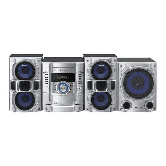
Photo: HCD-GX470
Model Name Using Similar Mechanism
CD
CD Mechanism Type
Section
Base Unit Name
Optical Pick-up Block Name
TAPE
Model Name Using Similar Mechanism
Section
Tape Transport Mechanism Type
Q Q
3
6 7
1 3
1 5
SPECIFICATIONS
COMPACT DISC DECK RECEIVER
co
.
9 4
2 8
US Model
Canadian Model
HCD-GX555
CDM74KF-K6BD83S
BU-K6BD83S-WOD
KSM-213DCP
NEW
CWN42FF609
0 5
8
2 9
9 4
2 8
CD player section
System: Compact disc and digital audio system
Laser Diode Properties
Emission duration: continuous
Laser Output*: Less than 44.6µW
*This output is the value measurement at a
distance of 200mm from the objective lens
surface on the Optical Pick-up Block with 7mm
aperture.
Frequency response: 20 Hz − 20 kHz
Signal-to-noise ratio: More than 90 dB
Dynamic range: More than 90 dB
Tape deck section
Recording system: 4-track 2-channel, stereo
Frequency response: 50 − 13,000 Hz (±3 dB),
using Sony TYPE I cassettes
– Continued on next page –
m
9 9
9 9
Advertisement
Table of Contents

Related Manuals for Sony HCD-GX470


Summary of Contents for Sony HCD-GX470
- Page 1 3 7 63 1515 0 SERVICE MANUAL US Model Canadian Model Ver. 1.3 2008.09 • HCD-GX470 is the amplifier, CD player, tape deck and tuner section in MHC-GX470. • HCD-GX570 is the amplifier, CD player, tape deck and tuner section in MHC-GX570. Photo: HCD-GX470...
-
Page 2: Leakage Test
THE PARTS LIST ARE CRITICAL TO SAFE OPERATION. FONCTIONNEMENT. NE REMPLACER CES COM- POSANTS REPLACE THESE COMPONENTS WITH SONY PARTS WHOSE QUE PAR DES PIÈCES SONY DONT LES NUMÉROS SONT PART NUMBERS APPEAR AS SHOWN IN THIS MANUAL OR DONNÉS DANS CE MANUEL OU DANS LES SUPPLÉMENTS IN SUPPLEMENTS PUBLISHED BY SONY. -
Page 3: Table Of Contents
HCD-GX470/GX570 3 7 63 1515 0 TABLE OF CONTENTS SERVICING NOTES EXPLODED VIEWS ..........4 8-1. Case Section ..............63 GENERAL 8-2. PANEL Board Section ............. 64 ..............5 8-3. Lid (Top) Section ............. 65 8-4. Front Panel Section ............66 DISASSEMBLY 8-5. -
Page 4: Servicing Notes
HCD-GX470/GX570 SECTION 1 SERVICING NOTES 3 7 63 1515 0 MODEL IDENTIFICATION NOTES ON HANDLING THE OPTICAL PICK-UP – Back Panel – BLOCK OR BASE UNIT Model number label The laser diode in the optical pick-up block may suffer electrostatic break-down because of the potential difference generated by the charged electrostatic load, etc. -
Page 5: General
HCD-GX470/GX570 SECTION 2 This section is extracted from instruction manual. GENERAL 3 7 63 1515 0 – GX470 – Guide to parts and AUDIO IN button qa PHONES jack Press to select the AUDIO IN function. Connect the headphones. -
Page 6: Basic Operations
HCD-GX470/GX570 3 7 63 1515 0 – GX570 – To turn on the subwoofer How to Subscribe Basic Operations XM $12.95 monthly service subscription sold separately. XM Press SUBWOOFER 5 on the unit repeatedly until Connect and Play (TM) antenna required to receive XM service (sold “SUB ON”... -
Page 7: Playing A Tape
HCD-GX470/GX570 3 7 63 1515 0 Notes on playing MP3 discs To select a channel using the number Notes on the display information • Do not save other types of files or unnecessary folders on a disc that • The following are not displayed;... -
Page 8: Other Operations
HCD-GX470/GX570 3 7 63 1515 0 Other Operations Recording onto a tape Using the Timers You can record on a TYPE I (normal) tape in two ways: The system offers three timer functions. You cannot activate both the Play Timer and the Rec Timer at the... -
Page 9: Disassembly
HCD-GX470/GX570 SECTION 3 DISASSEMBLY 3 7 63 1515 0 • This set can be disassembled in the order shown below. 3-1. DISASSEMBLY FLOW 3-2. CASE (SIDE-L), CASE (SIDE-R) (Page 10) 3-3. CASE (TOP) (Page 10) 3-4. LID (CD) (Page 10) 3-5. -
Page 10: Case (Side-L), Case (Side-R)
HCD-GX470/GX570 3 7 63 1515 0 Note: Follow the disassembly procedure in the numerical order given. 3-2. CASE (SIDE-L), CASE (SIDE-R) 3 case (side-L) 2 two screws (B3) 1 three screws (case 3 TP2) 6 case (side-R) 5 two screws... -
Page 11: Lid (Cd)
HCD-GX470/GX570 3 7 63 1515 0 3-4. LID (CD) 3 four claws 4 lid (CD) 1 Turn the gear (loading A) to the direction of the arrow. L 13942296513 3-5. CD MECHANISM DECK (CDM74KF-K6BD83S) 4 CD mechanism deck (CDM74KF-K6BD83S) -
Page 12: Front Panel Block
HCD-GX470/GX570 3 7 63 1515 0 3-6. FRONT PANEL BLOCK 1 flexible flat cable (19 core) (CN991) 5 front panel block 3 two connectors (CN301, CN302) 2 flexible flat cable (9 core) (CN061) L 13942296513 4 four screws (BVTP3 × 8) 3-7. -
Page 13: Back Panel Section
HCD-GX470/GX570 3 7 63 1515 0 3-8. BACK PANEL SECTION 5 back panel section 1 flexible flat cable (9 core) (tuner (FM/AM)) 3 flexible flat cable (15 core) (CN001) (GX570) 4 four screws 2 connector (B3) (CN041) 4 two screws... -
Page 14: Cd Board
HCD-GX470/GX570 3 7 63 1515 0 3-10. CD BOARD 1 two screws (BVTP2.6 × 8) 2 cover (OP) 5 CD board 4 Remove soldering from the four points. 3 flexible flat cable (16 core) (CN101) L 13942296513 3-11. DRIVE BOARD, SW BOARD 1 two screws (BTTP (M2.6)) -
Page 15: Optical Pick-Up Block
HCD-GX470/GX570 3 7 63 1515 0 3-12. OPTICAL PICK-UP BLOCK 1 floating screw (PTPWH M2.6) 5 two insulators 2 h older (213) assy qg optical pick-up block 4 two coil springs (insulator) 8 two insulators 7 two coil springs... -
Page 16: Motor (Tb) Board
HCD-GX470/GX570 3 7 63 1515 0 3-14. MOTOR (TB) BOARD 2 stopper 1 stopper 7 t able motor assy (M741) 3 wire (flat type) (5 core) (CN742) 8 MOTOR (TB) board 6 Remove the two solderings of motor. 5 two screws L 13942296513 (BTTP (M2.6)) -
Page 17: Test Mode
HCD-GX470/GX570 SECTION 4 TEST MODE 3 7 63 1515 0 COLD RESET AMP TEST MODE (GX470 ONLY) The cold reset clears all data including preset data stored in the This mode is used to display the parameter of amplifier IC and RAM to initial conditions. - Page 18 HCD-GX470/GX570 3 7 63 1515 0 VERSION DISPLAY MODE The 5th and 6th digit from the left indicates: (Present status display) This mode is used to check the model, destination and software The 5th and 6th digit from the left indicates which operating status version.
- Page 19 HCD-GX470/GX570 3 7 63 1515 0 2. Optical Pick-up Error Code Mode 5 REPEAT LIMIT CANCEL MODE When this mode is entered, optical pick-up error code is displayed Number of repeat for CD playback is 5 times when the repeat mode with the 8-character format on the fluorescent indicator tube.
-
Page 20: Mechanical Adjustments
HCD-GX470/GX570 SECTION 5 MECHANICAL ADJUSTMENTS 3 7 63 1515 0 PRECAUTION 1. Clean the following parts with a denatured-alcohol-moistened swab : record/playback head pinch roller erase head rubber belts capstan idlers 2. Demagnetize the record/playback head with a head demagnetizer. -
Page 21: Electrical Adjustments
HCD-GX470/GX570 SECTION 6 ELECTRICAL ADJUSTMENTS 3 7 63 1515 0 4. After the adjustments, apply suitable locking compound to DECK SECTION 0 dB=0.775 V the pats adjusted. 1. Demagnetize the record/playback head with a head Adjustment Location: Playback Head (DECK-A) demagnetizer. - Page 22 HCD-GX470/GX570 3 7 63 1515 0 Connecting Location: CD SECTION – CD Board (Conductor Side) – Note: 1. CD Block is basically constructed to operate without adjustment. 2. Use YEDS-18 disc (3-702-101-01) unless otherwise indicated. 3. Use an oscilloscope with more than 10 MΩ impedance.
-
Page 23: Diagrams
HCD-GX470/GX570 SECTION 7 3 7 6 3 1 5 1 5 0 DIAGRAMS 7-1. BLOCK DIAGRAM – CD SERVO Section – DETECTOR +3.3V CD-L (Page 24) 58 B AOUT1 RFACO 71 RFACI PCMD 4 PCMDI 59 C AOUT2 R-CH... -
Page 24: Block Diagram - Main Section
HCD-GX470/GX570 7-2. BLOCK DIAGRAM – MAIN Section – 3 7 6 3 1 5 1 5 0 (GX570) J001 XM RECEIVER D/A CONVERTER IC001 IC041 (XM) LINE AMP COMM_RX_P I2S_DA SDTI AOUTL IC051 D– COMM_RX_N AOUTR R-CH I2S_CLK BICK... -
Page 25: Block Diagram - Amp Section
HCD-GX470/GX570 3 7 6 3 1 5 1 5 0 7-3. BLOCK DIAGRAM – AMP Section – HP IN (Page 24) BASS AGC (Page 24) R-CH J701 PHONES R-CH JK441 –1 BUFFER POWER AMP (Page 24) IC251 IC441 –... -
Page 26: Block Diagram - Panel, Power Supply Section
HCD-GX470/GX570 3 7 6 3 1 5 1 5 0 7-4. BLOCK DIAGRAM – PANEL, POWER SUPPLY Section – PT901 MAIN POWER FLUORESCENT INDICATOR TUBE TRANSFORMER /LED DRIVER SYSTEM CONTROLLER IC701 (2/2) IC901 (4/4) I-VFD-DATA O-VFD-DATA D908 –27V S1 – S21... - Page 27 HCD-GX470/GX570 3 7 6 3 1 5 1 5 0 • Note For Printed Wiring Boards and Schematic Diagrams • Circuit Boards Location Note on Printed Wiring Board: Note on Schematic Diagram: • X : parts extracted from the component side.
-
Page 28: Printed Wiring Board - Cd Board
HCD-GX470/GX570 3 7 6 3 1 5 1 5 0 • See page 27 for Circuit Boards Location. 7-5. PRINTED WIRING BOARD – CD Board – : Uses unleaded solder. CD BOARD (COMPONENT SIDE) CD BOARD M401 (SPINDLE) (CONDUCTOR SIDE) -
Page 29: Schematic Diagram - Cd Board
HCD-GX470/GX570 3 7 6 3 1 5 1 5 0 • See page 51 for Waveforms. • See page 53 for IC Block Diagrams. • See page 56 for IC Pin Function Description. 7-6. SCHEMATIC DIAGRAM – CD Board –... -
Page 30: Printed Wiring Boards - Changer Section
HCD-GX470/GX570 3 7 6 3 1 5 1 5 0 • See page 27 for Circuit Boards Location. 7-7. PRINTED WIRING BOARDS – CHANGER Section – : Uses unleaded solder. • Semiconductor Location Ref. No. Location D701 D711 MOTOR (LD) BOARD... -
Page 31: Schematic Diagram - Changer Section
HCD-GX470/GX570 3 7 6 3 1 5 1 5 0 • See page 53 for IC Block Diagrams. 7-8. SCHEMATIC DIAGRAM – CHANGER Section – LOADING MOTOR DRIVE IC701 BA6956AN R702 R701 CN721 CN704 LM-2 LM-2 D701 M751 C751... -
Page 32: Printed Wiring Board - Deck Board
HCD-GX470/GX570 3 7 6 3 1 5 1 5 0 • See page 27 for Circuit Boards Location. 7-9. PRINTED WIRING BOARD – DECK Board – : Uses unleaded solder. • Semiconductor Location Ref. No. Location D301 D401 IC301... -
Page 33: Schematic Diagram - Deck Board
HCD-GX470/GX570 3 7 6 3 1 5 1 5 0 • See page 51 for Waveforms. 7-10. SCHEMATIC DIAGRAM – DECK Board – Q405,406,408 DECK-A/B SELECT SWITCH, REC/PB SELECT SWITCH R350 C315 R309 R489 (PB) (DECK-A) R306 R305 Q301... -
Page 34: Printed Wiring Board - Main Board
HCD-GX470/GX570 • See page 27 for Circuit Boards Location. 7-11. PRINTED WIRING BOARD – MAIN Board – : Uses unleaded solder. 3 7 6 3 1 5 1 5 0 • Semiconductor Location Ref. No. Location MAIN BOARD D001... -
Page 35: Schematic Diagram - Main Board (1/3)
HCD-GX470/GX570 • See page 51 for Waveforms. • See page 56 for IC Pin Function Description. 7-12. SCHEMATIC DIAGRAM – MAIN Board (1/3) – 3 7 6 3 1 5 1 5 0 (1/3) (GX570) C391 M+9V M-GND M-GND... -
Page 36: Schematic Diagram - Main Board (2/3)
HCD-GX470/GX570 3 7 6 3 1 5 1 5 0 • See page 53 for IC Block Diagrams. 7-13. SCHEMATIC DIAGRAM – MAIN Board (2/3) – (GX570) R304 R307 R306 Q302 (2/3) 470k 2.2k 2SC3052 Q303 CN333 (GX470) C308... -
Page 37: Schematic Diagram - Main Board (3/3)
HCD-GX470/GX570 3 7 6 3 1 5 1 5 0 7-14. SCHEMATIC DIAGRAM – MAIN Board (3/3) – (3/3) R265 Q261 R285 RT1P141C-TP-1 C259 R251 R274 R276 ∗R250,253 MUTING CONTROL SWITCH C265 4.7k Q271 4.7k(GX470) R263 R268 2SC3052 2.2k 4.7k... -
Page 38: Printed Wiring Board - Xm Board (Gx570)
HCD-GX470/GX570 3 7 6 3 1 5 1 5 0 • See page 27 for Circuit Boards Location. 7-15. PRINTED WIRING BOARD – XM Board (GX570) – : Uses unleaded solder. MAIN BOARD XM BOARD XM BOARD (COMPONENT SIDE) -
Page 39: Schematic Diagram - Xm Board (Gx570)
HCD-GX470/GX570 3 7 6 3 1 5 1 5 0 • See page 51 for Waveforms. • See page 53 for IC Block Diagrams. • See page 56 for IC Pin Function Description. 7-16. SCHEMATIC DIAGRAM – XM Board (GX570) –... -
Page 40: Printed Wiring Board - Mic. Aux. Hp Board
HCD-GX470/GX570 Ver. 1.2 3 7 6 3 1 5 1 5 0 • See page 27 for Circuit Boards Location. 7-17. PRINTED WIRING BOARD – MIC. AUX. HP Board – : Uses unleaded solder. (Page 34) MAIN BOARD MIC. AUX. HP BOARD... -
Page 41: Schematic Diagram - Mic. Aux. Hp Board
HCD-GX470/GX570 3 7 6 3 1 5 1 5 0 7-18. SCHEMATIC DIAGRAM – MIC. AUX. HP Board – R827 R823 2.2k J702 R825 O-HP/AUX AUDIO IN D-GND R826 R824 C820 C821 R832 R831 AUX-IN-RCH 1000p 1000p 470k 470k... -
Page 42: Printed Wiring Board - Power Board
HCD-GX470/GX570 3 7 6 3 1 5 1 5 0 • See page 27 for Circuit Boards Location. 7-19. PRINTED WIRING BOARD – POWER Board – : Uses unleaded solder. • Semiconductor TRANSFORMER (Page 49) BOARD Location CN903 Ref. No. Location... -
Page 43: Schematic Diagram - Power Board
HCD-GX470/GX570 3 7 6 3 1 5 1 5 0 7-20. SCHEMATIC DIAGRAM – POWER Board – R447 C441 R441 JW401 2.2k L441 R461 R411 R413 R412 IC441(1/2) STK403-130 L442 R434 C445 100p R462 R414 R497 R466 R465 Q481,482... -
Page 44: Printed Wiring Boards - Sub Woofer Section
HCD-GX470/GX570 3 7 6 3 1 5 1 5 0 • See page 27 for Circuit Boards Location. 7-21. PRINTED WIRING BOARDS – SUB WOOFER Section – : Uses unleaded solder. SW-SP BOARD (Page 42) POWER SUB WOOFER BOARD... -
Page 45: Schematic Diagram - Sub Woofer Section
HCD-GX470/GX570 3 7 6 3 1 5 1 5 0 7-22. SCHEMATIC DIAGRAM – SUB WOOFER Section – POWER AMP IC501 STK404-130 Q507 2SC3052 TEMPERATURE DETECT R511 R506 0.22 R530 R507 C508 4.7k 220p JW521 R510 0.22 R508 C507 4.7k... -
Page 46: Printed Wiring Board - Panel Board
HCD-GX470/GX570 Ver. 1.2 • See page 27 for Circuit Boards Location. 7-23. PRINTED WIRING BOARD – PANEL Board – : Uses unleaded solder. 3 7 6 3 1 5 1 5 0 • Semiconductor Location Ref. No. Location D711... -
Page 47: Printed Wiring Boards - Key Section
HCD-GX470/GX570 Ver. 1.2 • See page 27 for Circuit Boards Location. 7-24. PRINTED WIRING BOARDS – KEY Section – : Uses unleaded solder. 3 7 6 3 1 5 1 5 0 KEY LEFT BOARD KEY RIGHT BOARD D611 S601 –... -
Page 48: Schematic Diagram - Panel Section
HCD-GX470/GX570 Ver. 1.2 3 7 6 3 1 5 1 5 0 • See page 51 for Waveforms. • See page 56 for IC Pin Function Description. 7-25. SCHEMATIC DIAGRAM – PANEL Section – R745 4.7k FL701 R746 IC610... -
Page 49: Printed Wiring Board - Transformer Board
HCD-GX470/GX570 3 7 6 3 1 5 1 5 0 • See page 27 for Circuit Boards Location. 7-26. PRINTED WIRING BOARD – TRANSFORMER Board – : Uses unleaded solder. TRANSFORMER BOARD (AC IN) POWER BOARD CN442 (Page 42) -
Page 50: Schematic Diagram - Transformer Board
HCD-GX470/GX570 3 7 6 3 1 5 1 5 0 7-27. SCHEMATIC DIAGRAM – TRANSFORMER Board – R902 2.2M F904 1/2W (Page 43) CN903 T8AL 250V 240V F905 T8AL 250V C907 C908 220V F906 W901 T3.15A 250V JW909 JW902... -
Page 51: Http://Www.xiaoyu163.Com
HCD-GX470/GX570 3 7 63 1515 0 • Waveforms – CD Board – – DECK Board – – MAIN Board – Q453 (Base) (REC mode) IC201 1 (LRCK), 2 (LRCKI) IC901 qa (XT2 (32.768KHZ)) (CD play mode) 3 Vp-p 3.3 Vp-p 1.3 Vp-p... -
Page 52: Http://Www.xiaoyu163.Com
HCD-GX470/GX570 3 7 63 1515 0 – XM Board – – PANEL Board – IC001 wh (OSC_OUT) IC701 4 (X2) (XM mode) 3.5 Vp-p 3 Vp-p 22.2 ns 239 ns 1 V/DIV, 10 ns/DIV 1 V/DIV, 100 ns/DIV IC001 el (I2S_CLK) (XM mode) 4.5 Vp-p... -
Page 53: Http://Www.xiaoyu163.Com
HCD-GX470/GX570 3 7 63 1515 0 • IC Block Diagrams – CD Board – IC203 BH18LB1WG-TR VIN 1 THERMAL PROTECTION OVER CURRENT PROTECTION – VOLTAGE GND 2 REFERENCE VOUT CONTROL STBY 3 BLOCK IC402 BA5947FM-E2 MUTING L 13942296513 + –... -
Page 54: Http://Www.xiaoyu163.Com
HCD-GX470/GX570 3 7 63 1515 0 – MAIN Board – IC101 R2S15207FP 29 28 TONE CONTROL (BASS, TREBLE, MID) TONE RECOUT VOCALCUT ON/OFF ON/OFF VOLIN1 INA1 31 VOLUME INPUT SELECTOR BB11 GND 32 BB21 TONE ATT BASSBOOST ON/OFF REFIN 33... -
Page 55: Http://Www.xiaoyu163.Com
HCD-GX470/GX570 3 7 63 1515 0 – XM Board – IC041 AK4384ET-E2 DZFL DZFR CLOCK DE-ENPHASIS MCLK DRIVER CONTROL VCOM ∆Σ AOUTL BICK INTERPOLATOR MODULATOR AUDIO SDTI DATA INTERFACE LRCK ∆Σ AOUTR INTERPOLATOR MODULATOR SMUTE/CSN µP ACKS/CCLK INTERFACE DIF0/CDTI... -
Page 56: Http://Www.xiaoyu163.Com
HCD-GX470/GX570 3 7 63 1515 0 • IC Pin Function Description CD BOARD IC201 CXD3014A-201R (CD DSP) Pin No. Pin Name Description LRCK L/R sampling clock signal output terminal LRCKI L/R sampling clock signal input terminal PCMD Serial data output terminal... -
Page 57: Http://Www.xiaoyu163.Com
HCD-GX470/GX570 3 7 63 1515 0 Pin No. Pin Name Description FRDR Focus servo drive signal (-) output terminal IOVDD1 Power supply terminal (+3.3V) AVDD0 Power supply terminal (+3.3V) AVSS0 Ground terminal E signal input from the optical pick-up block... -
Page 58: Http://Www.xiaoyu163.Com
HCD-GX470/GX570 3 7 63 1515 0 Pin No. Pin Name Description SVDD Power supply terminal (+2.5V) JTAGTCK Clock signal input terminal (for JTAG) Not used JTAGTDI Data input terminal (for JTAG) Not used JTAGTDO Data output terminal (for JTAG) Not used... -
Page 59: Http://Www.xiaoyu163.Com
HCD-GX470/GX570 3 7 63 1515 0 MAIN BOARD IC901 uPD78F0547GC (S)-UBT-A (SYSTEM CONTROLLER) Pin No. Pin Name Description I-AC-PULSE AC power detection signal input terminal O-REC/PB Recording/playback selection signal output terminal "L": playback, "H": recording O-REC-MUTE Recording muting on/off control signal output terminal "L": muting on O-BIAS Recording bias on/off control signal output terminal "H": bias on... -
Page 60: Http://Www.xiaoyu163.Com
HCD-GX470/GX570 3 7 63 1515 0 Pin No. Pin Name Description I-SCOR Subcode sync (S0+S1) detection signal input from the CD DSP I-XM-IRQ Interrupt request signal input from the XM receiver (GX570) O-LC23003-CE Chip enable signal output to the tuner (FM/AM) -
Page 61: Http://Www.xiaoyu163.Com
HCD-GX470/GX570 3 7 63 1515 0 PANEL BOARD IC701 uPD780232GC-509-8BT-A (FLUORESCENT INDICATOR TUBE/LED DRIVER, TAPE MECHANISM DECK CONTROLLER) Pin No. Pin Name Description VDD1 Power supply terminal (+3.3V) VSS1 Ground terminal System clock input terminal (4.19 MHz) System clock output terminal (4.19 MHz) Input terminal for the IC test Normally: fixed at "L"... - Page 62 HCD-GX470/GX570 3 7 63 1515 0 XM BOARD IC001 F2602E-01-TR (XM RECEIVER) (GX570) Pin No. Pin Name Description LSDP_TXRX Not used Ground terminal SC_XT_OUT Serial data output to the system controller Power supply terminal (+3.3V) SC_RX_IN Serial data input from the system controller...
-
Page 63: Exploded Views
HCD-GX470/GX570 SECTION 8 EXPLODED VIEWS 3 7 63 1515 0 NOTE: • -XX and -X mean standardized parts, so they • Items marked “*” are not stocked since they The components identified by mark 0 or dotted line with mark 0 are may have some difference from the original are seldom required for routine service. -
Page 64: Panel Board Section
HCD-GX470/GX570 3 7 63 1515 0 8-2. PANEL BOARD SECTION lid (top) section L 13942296513 Ref. No. Part No. Description Remark Ref. No. Part No. Description Remark 2-658-294-11 KNOB (JOG) 2-658-281-01 KEY (JOG) 2-658-293-01 KNOB (VOL B) (GROOVE, SURROUND, ENTER, EQ BAND) -
Page 65: Lid (Top) Section
HCD-GX470/GX570 3 7 63 1515 0 8-3. LID (TOP) SECTION not supplied not supplied L 13942296513 front panel section Ref. No. Part No. Description Remark Ref. No. Part No. Description Remark 2-658-285-13 REFLECTOR (VOL) 2-658-287-11 KEY (CENTER R) (s, L TUNING +,... -
Page 66: Front Panel Section
HCD-GX470/GX570 3 7 63 1515 0 8-4. FRONT PANEL SECTION not supplied not supplied supplied not supplied not supplied not supplied L 13942296513 Ref. No. Part No. Description Remark Ref. No. Part No. Description Remark 2-658-304-01 SPRING (CASS R) 4-951-620-01 SCREW (2.6X8), +BVTP... -
Page 67: Main Board Section
HCD-GX470/GX570 3 7 63 1515 0 8-5. MAIN BOARD SECTION (GX570) supplied M001 POWER board, SUB WOOFER board section not supplied (SW-SP board) L 13942296513 chassis section Ref. No. Part No. Description Remark Ref. No. Part No. Description Remark... -
Page 68: Power Board, Sub Woofer Board Section
HCD-GX470/GX570 3 7 63 1515 0 8-6. POWER BOARD, SUB WOOFER BOARD SECTION not supplied not supplied not supplied L 13942296513 not supplied not supplied Ref. No. Part No. Description Remark Ref. No. Part No. Description Remark u163 A-1163-222-A POWER BOARD, COMPLETE (GX570) -
Page 69: Chassis Section
HCD-GX470/GX570 3 7 63 1515 0 8-7. CHASSIS SECTION F904 PT901 F907 F905 F906 not supplied L 13942296513 supplied supplied not supplied Ref. No. Part No. Description Remark Ref. No. Part No. Description Remark 0 F904 1-533-949-33 FUSE, CYLINDRICAL (TIME LUG) (T8AL/250V) -
Page 70: Cd Mechanism Deck Section-1 (Cdm74Kf-K6Bd83S)
HCD-GX470/GX570 3 7 63 1515 0 8-8. CD MECHANISM DECK SECTION-1 (CDM74KF-K6BD83S) L 13942296513 M741 CD mechanism deck section-2 Ref. No. Part No. Description Remark Ref. No. Part No. Description Remark 4-218-253-62 SCREW (M2.6), +BTTP 4-243-820-01 GEAR (TABLE) 1-828-938-51 WIRE (FLAT TYPE) (5 CORE) -
Page 71: Cd Mechanism Deck Section-2 (Cdm74Kf-K6Bd83S)
HCD-GX470/GX570 3 7 63 1515 0 8-9. CD MECHANISM DECK SECTION-2 (CDM74KF-K6BD83S) S711 M751 included in 579 included in 579 (spinlde motor L 13942296513 (sled motor (M401)) (M402)) S101 Ref. No. Part No. Description Remark Ref. No. Part No. -
Page 72: Electrical Parts List
HCD-GX470/GX570 SECTION 9 3 7 63 1515 0 ELECTRICAL PARTS LIST NOTE: • Due to standardization, replacements in the • Items marked “*” are not stocked since they The components identified by mark are seldom required for routine service. - Page 73 HCD-GX470/GX570 DECK 3 7 63 1515 0 Ref. No. Part No. Description Remark Ref. No. Part No. Description Remark A-1171-482-A DECK BOARD, COMPLETE < TRANSISTOR > ********************* Q321 6-551-120-01 TRANSISTOR 2SA2119K < CAPACITOR/RESISTOR > < RESISTOR/FERRITE BEAD > C301 1-162-964-11 CERAMIC CHIP 0.001uF...
- Page 74 HCD-GX470/GX570 DECK 3 7 63 1515 0 Ref. No. Part No. Description Remark Ref. No. Part No. Description Remark < CONNECTOR > R306 1-216-849-11 METAL CHIP 220K 1/10W R307 1-216-829-11 METAL CHIP 4.7K 1/10W CN008 1-568-830-11 CONNECTOR, FFC 11P...
- Page 75 HCD-GX470/GX570 Ver. 1.2 DECK DRIVER KEY LEFT 3 7 63 1515 0 Ref. No. Part No. Description Remark Ref. No. Part No. Description Remark R445 1-216-864-11 SHORT CHIP < TRANSISTOR > R446 1-216-864-11 SHORT CHIP Q731 8-729-029-66 TRANSISTOR DTC114ESA...
- Page 76 HCD-GX470/GX570 KEY RIGHT MAIN 3 7 63 1515 0 Ref. No. Part No. Description Remark Ref. No. Part No. Description Remark C063 1-164-156-11 CERAMIC CHIP 0.1uF A-1159-681-A KEY RIGHT BOARD, COMPLETE C064 1-162-964-11 CERAMIC CHIP 0.001uF ************************** C065 1-162-964-11 CERAMIC CHIP 0.001uF...
- Page 77 HCD-GX470/GX570 Ver. 1.3 MAIN 3 7 63 1515 0 Ref. No. Part No. Description Remark Ref. No. Part No. Description Remark C260 1-124-261-00 ELECT 10uF < CONNECTOR > C263 1-126-935-11 ELECT 470uF C264 1-162-964-11 CERAMIC CHIP 0.001uF * CN031...
- Page 78 HCD-GX470/GX570 MAIN 3 7 63 1515 0 Ref. No. Part No. Description Remark Ref. No. Part No. Description Remark R006 1-216-829-11 METAL CHIP 4.7K 1/10W < JUMPER RESISTOR > R008 1-216-833-11 METAL CHIP 1/10W JR101 1-216-864-11 SHORT CHIP (GX570)
- Page 79 HCD-GX470/GX570 MAIN 3 7 63 1515 0 Ref. No. Part No. Description Remark Ref. No. Part No. Description Remark R253 1-216-829-11 METAL CHIP 4.7K 1/10W R125 1-216-829-11 METAL CHIP 4.7K 1/10W R126 1-216-829-11 METAL CHIP 4.7K 1/10W (GX470) R253...
- Page 80 HCD-GX470/GX570 MAIN 3 7 63 1515 0 Ref. No. Part No. Description Remark Ref. No. Part No. Description Remark R901 1-216-845-11 METAL CHIP 100K 1/10W R316 1-216-809-11 METAL CHIP 1/10W R317 1-216-809-11 METAL CHIP 1/10W R902 1-216-864-11 SHORT CHIP...
- Page 81 HCD-GX470/GX570 MAIN MIC. AUX. HP MOTOR (LD) MOTOR (TB) PANEL 3 7 63 1515 0 Ref. No. Part No. Description Remark Ref. No. Part No. Description Remark R978 1-216-809-11 METAL CHIP 1/10W (GX570) < CAPACITOR > R979 1-216-809-11 METAL CHIP...
- Page 82 HCD-GX470/GX570 PANEL POWER 3 7 63 1515 0 Ref. No. Part No. Description Remark Ref. No. Part No. Description Remark R773 1-216-821-11 METAL CHIP 1/10W < RESISTOR > R774 1-216-833-11 METAL CHIP 1/10W R775 1-216-821-11 METAL CHIP 1/10W R607...
- Page 83 HCD-GX470/GX570 POWER SENSOR 3 7 63 1515 0 Ref. No. Part No. Description Remark Ref. No. Part No. Description Remark R441 1-216-825-11 METAL CHIP 2.2K 1/10W < CONNECTOR > R442 1-216-825-11 METAL CHIP 2.2K 1/10W R443 1-216-841-11 METAL CHIP...
- Page 84 HCD-GX470/GX570 SENSOR SUB WOOFER SW-SP TRANSFOMER 3 7 63 1515 0 Ref. No. Part No. Description Remark Ref. No. Part No. Description Remark 0 R505 < IC > 1-215-873-00 METAL OXIDE 4.7K (GX470) IC731 6-600-022-01 IC RPI-576 0 R505 1-215-896-00 METAL OXIDE 4.7K...
- Page 85 HCD-GX470/GX570 TRANSFOMER 3 7 63 1515 0 Ref. No. Part No. Description Remark Ref. No. Part No. Description Remark C910 1-126-968-11 ELECT 100uF C018 1-162-915-11 CERAMIC CHIP 10PF 0.5PF C911 1-126-942-61 ELECT 1000uF C019 1-162-915-11 CERAMIC CHIP 10PF 0.5PF...
- Page 86 HCD-GX470/GX570 3 7 63 1515 0 Ref. No. Part No. Description Remark Ref. No. Part No. Description Remark R002 1-216-845-11 METAL CHIP 100K 1/10W 1-832-404-21 CABLE, FLEXIBLE FLAT (16 CORE) R003 1-216-845-11 METAL CHIP 100K 1/10W 0 579 A-4735-357-A OPTICAL PICK-UP BLOCK (KSM-213DHAP)
- Page 87 HCD-GX470/GX570 3 7 63 1515 0 US Model Canadian Model SERVICE MANUAL Ver. 1.1 2006.04 SUPPLEMENT-1 File this supplement with the service manual. Subject: Change of DECK board (Suffix-12) In this set, DECK board has been changed in the midway of production.
- Page 88 HCD-GX470/GX570 3 7 63 1515 0 DIAGRAMS • Note for Printed Wiring Boards and Schematic Diagrams Note on Printed Wiring Board: Note on Schematic Diagram: • X : parts extracted from the component side. • All capacitors are in µF unless otherwise noted. (p: pF) •...
- Page 89 HCD-GX470/GX570 3 7 6 3 1 5 1 5 0 • Semiconductor 2-1. PRINTED WIRING BOARD – DECK Board – : Uses unleaded solder. Location Ref. No. Location D301 D401 IC301 IC401 (Refer to page 34 on service manual)
- Page 90 HCD-GX470/GX570 3 7 6 3 1 5 1 5 0 2-2. SCHEMATIC DIAGRAM – DECK Board – Q405,406,408 Q301 DECK-A/B SELECT SWITCH, 2SJ460 PB SWITCH REC/PB SELECT SWITCH R350 C315 R309 (DECK-A) R489 (PB) (DECK-A) R306 R305 CN301 220k...
- Page 91 HCD-GX470/GX570 DECK 3 7 63 1515 0 ELECTRICAL PARTS LIST NOTE: • Due to standardization, replacements in the • Items marked “*” are not stocked since they When indicating parts by reference number, please include the board. parts list may be different from the parts are seldom required for routine service.
- Page 92 HCD-GX470/GX570 DECK 3 7 63 1515 0 Ref. No. Part No. Description Remark Ref. No. Part No. Description Remark R407 1-216-829-11 METAL CHIP 4.7K 1/10W < TRANSISTOR > R408 1-216-829-11 METAL CHIP 4.7K 1/10W Q301 6-550-290-01 FET 2SJ460-T R409...
- Page 93 HCD-GX470/570 HCD-GX470/GX570 3 7 6 3 1 5 1 5 0 DIAGRAMS • Note for Printed Wiring Boards and Schematic Diagrams Note on Printed Wiring Board: Note on Schematic Diagram: • X : parts extracted from the component side.
- Page 94 HCD-GX470/GX570 2-1. PRINTED WIRING BOARD – MAIN Board – :Uses unleaded solder. 3 7 6 3 1 5 1 5 0 • Semiconductor Location MAIN BOARD Ref. No. Location D001 D002 (GX570) JW107 D003 JW109 ANTENNA D004 JW113 D005 FM75Ω...
- Page 95 HCD-GX470/GX570 3 7 6 3 1 5 1 5 0 2-2. SCHEMATIC DIAGRAM – MAIN Board (1/3) – (1/3) (GX570) C391 M+9V M-GND M-GND C-LR LM-R C-LF LM-F C-TR TM-R C-TF TM-F R952 C-E1 CN991 C-E2 C-E3 (GX570) C-SE...
- Page 96 HCD-GX470/GX570 3 7 6 3 1 5 1 5 0 2-3. SCHEMATIC DIAGRAM – MAIN Board (2/3) – (GX570) R304 R307 R306 Q302 (2/3) 470k 2.2k 2SC3052 Q303 CN333 (GX470) C308 RT1P141C-TP-1 R327 R311 R313 R357 MUTING CONTROL R360...
- Page 97 HCD-GX470/GX570 3 7 6 3 1 5 1 5 0 2-4. SCHEMATIC DIAGRAM – MAIN Board (3/3) – (3/3) R265 Q261 R285 RT1P141C-TP-1 C259 R251 R274 R276 ∗R250,253 MUTING CONTROL SWITCH C265 4.7k Q271 4.7k(GX470) R263 R268 2SC3052 2.2k 4.7k...
- Page 98 HCD-GX470/GX570 3 7 6 3 1 5 1 5 0 2-5. PRINTED WIRING BOARD – KEY RIGHT Board – :Uses unleaded solder. 2-6. SCHEMATIC DIAGRAM – KEY RIGHT Board – TO PANEL BOARD CN604 KEY RIGHT BOARD CN605 S624, S631 –...
- Page 99 HCD-GX470/GX570 KEY RIGHT MAIN 3 7 63 1515 0 ELECTRICAL PARTS LIST NOTE: • Due to standardization, replacements in the • Items marked “*” are not stocked since they The components identified by mark 0 or dotted line with mark 0 are parts list may be different from the parts are seldom required for routine service.
- Page 100 HCD-GX470/GX570 MAIN 3 7 63 1515 0 Ref. No. Part No. Description Remark Ref. No. Part No. Description Remark C141 1-126-964-11 ELECT 10uF C332 1-126-960-11 ELECT C142 1-126-964-11 ELECT 10uF (GX570) C143 1-137-374-11 MYLAR 0.047uF C385 1-162-927-11 CERAMIC CHIP...
- Page 101 HCD-GX470/GX570 Ver. 1.3 MAIN 3 7 63 1515 0 Ref. No. Part No. Description Remark Ref. No. Part No. Description Remark Q045 8-729-120-28 TRANSISTOR 2SC1623-L5L6 D031 8-719-988-61 DIODE 1SS355TE-17 D035 8-719-000-08 DIODE MC2838 Q046 8-729-045-62 FET 2SK2158-T2B D036 8-719-000-07 DIODE MC2836...
- Page 102 HCD-GX470/GX570 MAIN 3 7 63 1515 0 Ref. No. Part No. Description Remark Ref. No. Part No. Description Remark R157 1-216-849-11 METAL CHIP 220K 1/10W R056 1-216-833-11 METAL CHIP 1/10W R057 1-216-821-11 METAL CHIP 1/10W 0 R059 1-215-892-11 METAL OXIDE...
- Page 103 HCD-GX470/GX570 MAIN 3 7 63 1515 0 Ref. No. Part No. Description Remark Ref. No. Part No. Description Remark R354 1-216-837-11 METAL CHIP 1/10W R289 1-216-845-11 METAL CHIP 100K 1/10W (GX470) R290 1-216-821-11 METAL CHIP 1/10W R291 1-216-817-11 METAL CHIP...
- Page 104 HCD-GX470/GX570 MAIN 3 7 63 1515 0 Ref. No. Part No. Description Remark Ref. No. Part No. Description Remark R948 1-216-825-11 METAL CHIP 2.2K 1/10W R949 1-216-833-11 METAL CHIP 1/10W R950 1-216-829-11 METAL CHIP 4.7K 1/10W R952 1-216-841-11 METAL CHIP...
- Page 105 HCD-GX470/GX570 3 7 63 1515 0 MEMO L 13942296513 u163 http://www.xiaoyu163.com...
- Page 106 HCD-GX470/GX570 3 7 63 1515 0 REVISION HISTORY Clicking the version allows you to jump to the revised page. Also, clicking the version at the top of the revised page allows you to jump to the next revised page.