Table of Contents
Advertisement
Quick Links
SERVICE MANUAL
4
2006
MA254
KD-AVX2J,KD-AVX2E,KD-AVX2EU,
KD-AVX2EE,KD-AVX2U,KD-AVX2UN,
Lead free solder used in the board (material : Sn-Ag-Cu, melting point : 219 Centigrade)
1
PRECAUTIONS . . . . . . . . . . . . . . . . . . . . . . . . . . . . . . . . . . . . . . . . . . . . . . . . . . . . . . . . . . . . . . . . . . . . . . . 1-4
2
SPECIFIC SERVICE INSTRUCTIONS . . . . . . . . . . . . . . . . . . . . . . . . . . . . . . . . . . . . . . . . . . . . . . . . . . . . . . 1-7
3
DISASSEMBLY . . . . . . . . . . . . . . . . . . . . . . . . . . . . . . . . . . . . . . . . . . . . . . . . . . . . . . . . . . . . . . . . . . . . . . . 1-8
4
ADJUSTMENT . . . . . . . . . . . . . . . . . . . . . . . . . . . . . . . . . . . . . . . . . . . . . . . . . . . . . . . . . . . . . . . . . . . . . . . 1-23
5
TROUBLESHOOTING . . . . . . . . . . . . . . . . . . . . . . . . . . . . . . . . . . . . . . . . . . . . . . . . . . . . . . . . . . . . . . . . . 1-33
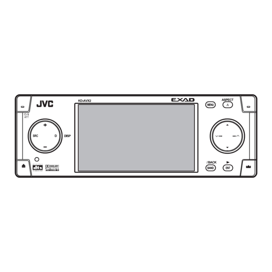
DVD/CD RECEIVER
KD-AVX2A
TABLE OF CONTENTS
COPYRIGHT © 2006 Victor Company of Japan, Limited
A
No.MA254
2006/4
Advertisement
Table of Contents

Related Manuals for JVC KD-AVX2J


Summary of Contents for JVC KD-AVX2J
-
Page 1: Table Of Contents
SERVICE MANUAL DVD/CD RECEIVER MA254 2006 KD-AVX2J,KD-AVX2E,KD-AVX2EU, KD-AVX2EE,KD-AVX2U,KD-AVX2UN, KD-AVX2A Lead free solder used in the board (material : Sn-Ag-Cu, melting point : 219 Centigrade) TABLE OF CONTENTS PRECAUTIONS ............... 1-4 SPECIFIC SERVICE INSTRUCTIONS . - Page 2 SPECIFICATION AUDIO AMPLIFIER SECTION × Ω Power Output Only the United States 20 W RMS 4 Channels at 4 and [< or =] 1% THD+N Ω Signal to Noise Ratio Only the United States 80 dBA (reference: 1 W into 4 In countries other than the United States 70 dB Maximum Power Output...
- Page 3 DVD/CD PLAYER SECTION Signal Detection System Non-contact optical pickup (semiconductor laser) Number of Channels 2 channels (stereo) Frequency Response DVD fs=48 kHz 16 Hz to 22 000 Hz DVD fs=192 kHz 16 Hz to 88 000 Hz VCD, CD 16 Hz to 20 000 Hz Dynamic Range 93 dB Signal-to-Noise Ratio...
-
Page 4: Precautions
SECTION 1 PRECAUTIONS Safety Precautions Burrs formed during molding may be left over on some parts of the chassis. Therefore, pay attention to such burrs in the case of preforming repair of this system. Please use enough caution not to see the beam directly or touch it in case of an adjustment or operation check. - Page 5 Preventing static electricity Electrostatic discharge (ESD), which occurs when static electricity stored in the body, fabric, etc. is discharged, can destroy the laser diode in the traverse unit (optical pickup). Take care to prevent this when performing repairs. 1.2.1 Grounding to prevent damage by static electricity Static electricity in the work area can destroy the optical pickup (laser diode) in devices such as laser products.
- Page 6 Important for laser products 5.CAUTION : If safety switches malfunction, the laser is able 1.CLASS 1 LASER PRODUCT to function. 2.DANGER : Invisible laser radiation when open and inter 6.CAUTION : Use of controls, adjustments or performance of lock failed or defeated. Avoid direct exposure to beam. procedures other than those specified here in may result in 3.CAUTION : There are no serviceable parts inside the hazardous radiation exposure.
-
Page 7: Specific Service Instructions
SECTION 2 SPECIFIC SERVICE INSTRUCTIONS This service manual does not describe SPECIFIC SERVICE INSTRUCTIONS. (No.MA254)1-7... -
Page 8: Disassembly
SECTION 3 DISASSEMBLY Main body section 3.1.1 Removing the panel assembly (See Fig.1) (1) Push the button(detach) in the lower right part of the panel assembly. Panel assembly (2) Remove the panel assembly. Button(detach) Fig.1 3.1.2 Removing the side heat sink (See Fig.2) Reference: Remove the panel assembly as required. - Page 9 3.1.3 Removing the top chassis assembly (See Figs.3 to 6) • Remove the panel assembly and side heat sink. (1) From the top side of the main body, remove the two screws Bottom chassis assembly C attaching the top chassis assembly. (See Fig.3.) (2) From the both sides of the main body, remove the two screws D attaching the top chassis assembly.
-
Page 10: Top Chassis Assembly Fig
3.1.4 Removing the front chassis assembly (See Fig.7 and 8) • Remove the panel assembly, side heat sink and top chassis assembly. Top chassis assembly (1) From the both sides of the top chassis assembly, remove the two screws E attaching the front chassis assembly. (See Fig.7 and 8.) (2) Remove the front chassis assembly from the top chassis assembly. - Page 11 3.1.6 Removing the connection control board (See Fig.10) • Remove the panel assembly, side heat sink, top chassis as- sembly and DVD mechanism assembly. Connection control board (1) From the top side of the DVD mechanism assembly, re- lease the lock of the connector CN965 on the connection CN965...
- Page 12 3.1.7 Removing the rear bracket (See Fig.11 to 13) • Remove the panel assembly, side heat sink and top chassis assembly. Wire holder Rear bracket (1) Remove the screw J, screw J', two screws K and screw M attaching the rear bracket. (See Fig. 11.) Reference: When attaching the screw J', attach the wire holder with it as before.
- Page 13 3.1.9 Removing the front door mechanism assembly (See Fig.14) • Remove the front panel assembly, side heat sink, top chassis assembly main board and rear bracket. Front door mechanism assembly (1) From the top side of the bottom chassis assembly, remove Bottom chassis the screw Q attaching the FPC guide to the bottom chassis.
- Page 14 DVD mechanism assembly 3.2.1 Removing the mechanism control board (See Fig.1) Caution: Before disconnecting the flexible wire extending from the DVD Lug wire Flexible wire pickup, solder the short-circuit point on the flexible wire using Feed motor a grounding soldering iron. If you do not follow this instruction, Double tape the DVD pickup may be damaged.
- Page 15 3.2.2 Removing the top cover (See Fig.2) (1) Remove the two screws D attaching the top cover on the back of the body. (2) Remove the top cover upward. Reference: When reassembling, set part b of the top cover under the bending part c of the chassis frame.
- Page 16 3.2.4 Removing the clamper unit (See Fig.5 to 7) • Remove the top cover and the mechanism section. (1) Remove the clamper2 spring on the bottom of the mecha- Clamper2 spring nism section. (See Figs.5.and 6.) (2) Release the part d of the clamper spring from the bending part of the chassis base assembly.
- Page 17 Clamper unit Clamper spring Fig.8 Clamper unit Notch Fig.9 (No.MA254)1-17...
- Page 18 3.2.6 Removing the front unit (See Fig.10 to 12) • Remove the top cover and the mechanism section. (1) Disconnect the flexible wire from connector CN202 on the mechanism control board at the bottom of the body. (See Front unit Fig.10.) (2) Remove the screw G attaching the front unit on the top of the body.
- Page 19 3.2.7 Removing the loading arm assembly (See Fig.13 , 14) • Remove the top cover, the mechanism section and the front unit. (1) From the top of the body, move the loading arm assembly from the front side upward, and release the bosses from the right and left joints k and m of the chassis base assem- bly.
- Page 20 3.2.8 Removing the rod (L)(R)/roller assembly (See Fig.15 and 16) • Remove the top cover, the mechanism section, the front unit and the loading arm assembly. Collar Collar (1) Release the rod (L) and (R) from the joints q at the bottom of the loading arm assembly (See Fig.15.) (2) Remove the roller assembly from the loading arm assem- bly.
- Page 21 3.2.9 Removing the DVD pickup assembly (See Fig.17 to 19) • Remove the mechanism control board. (1) From the bottom of the body, turn the feed gear in the di- Feed gear rection of the arrow to move the DVD pickup outwards. (See Fig.17.) (2) Remove the screw J attaching the thrust spring.
- Page 22 3.2.10 Removing the spindle motor (See Fig.20) • Remove the mechanism control board. Remove the two screws L attaching the spindle motor on the Spindle motor bottom of the body. Caution: Perform adjustment when reattaching the spindle motor. Fig.20 3.2.11 Removing the feed motor assembly (See Fig.21 and 22) •...
-
Page 23: Adjustment
SECTION 4 ADJUSTMENT Test instruments required for adjustment Standard measuring conditions (1) Digital oscilloscope (100MHz) Power supply voltage DC14.4V(11 to 16V) (2) Jitter meter 4 Ω (2 Speakers connection) Load impedance (3) Digital tester 20K Ω Line Output (4) Electric voltmeter (5) Tracking offset meter Caution: (6) Test Disc : VT501 or VT502... - Page 24 Adjustment method for jitter After replacing the pickup, set the unit in the service mode to display a jitter value on the LCD. Confirm that the jitter value measured with a jitter meter is within 12% of the jitter value displayed on the LCD. If it is within 12%, then adjustment is not necessary.
- Page 25 Jitter value conversion table Load the test DVD and set the unit to the service mode. A jitter value converted to the hex value is displayed on the LCD. Refer to the corresponding decimal notation value shown in the following Jitter Conversion Table. The adjustment is OK if the jitter value measured with a jitter meter is within 12% of the jitter value displayed on the LCD.
- Page 26 Service mode 4.6.1 Service mode 1 (Indication of a service mode 1 is nothing.) Keep this state more 2 seconds while continuing pressing the [STANDBY/ON ATTENUATOR] button and [EJECT] button sequentially. Screen indication Exchanging it operate a menu of a service mode with the [UP] button and NO EJECT? [DOWN] button.
- Page 27 INITIALIZE (Initialization of a user area of each EEPROM Main micon EEPROM initialization (a user entry domain and picture adjustment data) DVD unit EEPROM initialization (except a permanent domain) After clear completion, a screen returns to service mode indication after OK indication was displayed for three seconds.
- Page 28 DVD NTSC/PAL DVD picture change NTSC JD4 output picture setting (NTSC) JD4 output picture setting (PAL) DVD CHECK MODE See "DVD CHECK MODE" for details. ERROR READ DVD ERROR READ CH ERROR READ MECHA ERROR READ READ ALL DVD ERROR READ Reading of a DVD unit error history CH ERROR READ Reading of a CD changer error history...
- Page 29 DVD check mode DVD CHECK MODE DVD CHECK MODE DVD CHECK MODE NORMAL PLAY EEPROM DATA DISP STOP EF OUT-TRACKING OFF EEPROM DATA CLEAR OPEN EF IN-TRACKING OFF TEMPERATURE CD-LASER ON SEARCH & JITTER DVD-LASER ON MONITOR DVDx1 JITTER MODE PLAY Exchanging it operate a menu of a service mode with the [UP] button.
- Page 30 Error code tables 4.8.1 Mechanism error code Error contents Details Error code Detailed error code Disc loading error B1 time out 0x09 0x0011 C1 time out 0x09 0x0012 D1 time out 0x09 0x0013 C2 time out 0x09 0x0014 B2 time out 0x09 0x0015 A2 time out...
- Page 31 Running mode Indication Explanation Operation contents of 1 cycle In mecha error In mecha error RUNNING1 MECHA Door mecha running 1 Panel close Panel open RUNNING2 MECHA Door mecha running 2 Panel close Panel open Panel detach position RETRY Retry Panel angle 3 position Panel angle 1...
- Page 32 4.10 Monitor adjustment * When adjusting, switch on the main unit and insert a test disc (VT-501). And play the test disc and pause it. (1) Set the service mode 4. (2) Exchanging it operate a menu of a service mode with the [UP] button and [DOWN] button. (3) Change data with the [B.SKIP]/[F.SKIP] buttons.
-
Page 33: Troubleshooting
SECTION 5 TROUBLESHOOTING Feed section Is 4V present at both Check the feed motor. sides of the feed motor? Check the connections Is the voltage output at between the feed motor pin 17 and pin 18 of IC201? and IC201. Is the power supply Is the voltage input at pin present at pin 14... - Page 34 Spindle section Is the disk rotated? Is the voltage output at Check the connection between pins 20,22,24 of IC251? the CN201 and card wire. Is the power supply Is the voltage input at pin present at pin 14 Check IC251. 17 of IC251? of IC251? Check the voltage output...
- Page 35 Signal processing section Is the sound output from Normal both channels (L, R)? Is the audio signal (including sampling Is the audio signal output No sound from either Is 9V present at pin 42 output components) at pins 28,29,32,33 of channel.
- Page 36 16 PIN CORD DIAGRAM (for KD-AVX2J,KD-AVX2U,KD-AVX2UN,KD-AVX2A) GN/BK WH/BK Black Green VI/BK GY/BK Violet Gray Blue White Yellow BL/WH L. GN Orange Brown OR/WH L.GN Light Green GN/BK WH/BK VI/BK GY/BK BL/WH REMOTE TEL MUTING OR/WH ILLUMINATION CONTROL Choking Coil MEMORY L.GN...
- Page 37 16 PIN CORD DIAGRAM (for KD-AVX2E,KD-AVX2EU,KD-AVX2EE) Black Green GN/BK WH/BK Violet VI/BK GY/BK Gray Blue White Yellow Orange Brown BL/WH L. GN L.GN Light Green OR/WH BL/WH OR/WH Choking Coil MEMORY REMOTE BL/WH OR/WH VI/BK GY/BK WH/BK GN/BK L.GN PARKING PARKING BRAKE REVERS...
- Page 38 Victor Company of Japan, Limited Mobile Entertainment Business Group Mobile Entertainment Category 10-1,1chome,Ohwatari-machi,Maebashi-city,Gumma-ken, 371-8543,Japan (No.MA254) Printed in Japan...
- Page 39 SCHEMATIC DIAGRAMS DVD/CD PLAYER KD-AVX2J,KD-AVX2E,KD-AVX2EU KD-AVX2EE,KD-AVX2U,KD-AVX2UN KD-AVX2A CD-ROM No.SML200604 Lead free solder used in the board (material : Sn-Ag-Cu, melting point : 219 Centigrade) Contents Block diagram Standard schematic diagrams Printed circuit boards 2-8 to 10 No.MA254SCH COPYRIGHT 2006 Victor Company of Japan, Limited.
-
Page 40: Safety Precaution
Safety precaution Burrs formed during molding may be left over on some parts of the chassis. Therefore, pay attention to such burrs in the case of preforming repair of this system. Please use enough caution not to see the beam directly or touch it in case of an adjustment or operation check. -
Page 41: Block Diagram
I/O, BUSINT EEP_DAI AV BUS SW4,SW5 SW1,SW4 IC721 BUSSO, BUSSCK EEP_DAO IC941 L-END SW EPROM SI/SO REST SW JVC BUS CN871 IC731 ST_REM RESET OE REMOTE RESET PNL_KEY Used for Area suffix J/E/EU/EE IC741 D991,Q701 KEYDATA LCD & Key control section... -
Page 42: Standard Schematic Diagrams
Standard schematic diagrams SUB.W.OUT LINE IN CENTER.OUT D312 C N 3 1 1 Q G A 2 5 0 1 C 1 - 0 6 MA111-X Mian section (1) C 3 4 5 R 3 4 7 R 3 4 4 2nd AUDIO C E N T E R MUTING... - Page 43 C - P A N E L R 9 9 2 3 RB051L-40-X 0 . 0 1 SWREG3.3V IC824 BD9781HFP-W PANEL.DRIVER JVC BUS IC881 R 9 9 2 4 BA6956AN R 9 4 5 R 9 9 2 1 4 7 0 1 0 k...
- Page 44 Panel section (1) R T 1 N 1 4 1 C 1 0 K 1 0 K 2 4 2 3 2 2 2 1 2 0 1 9 1 8 1 7 1 6 1 5 1 4 1 3 1 2 1 1 1 0 R T 1 P 1 4 1 C 1 0 K I C 6 4 1...
- Page 45 Panel section (2) D 5 0 0 1 U D Z W 2 4 B - X D 5 0 0 2 U D Z W 5 . 6 B - X D 5 0 2 0 U D Z W 5 . 6 B - X D 5 0 0 3 U D Z W 5 .
- Page 46 Connection section R 9 0 6 1 2 2 k C 9 0 2 1 R 9 0 1 8 0 . 0 0 1 8 R 9 0 6 2 4 . 7 k 4 . 7 k R 9 0 5 8 R 9 0 1 9 R 9 0 4 3 1 0 0...
- Page 47 DVD section D3.3V P3.3V R300 IC303 IC399 EDS1232AATA-75 R301 P3.3V K301 C391 K399 IC398 SG32M90TFIR3 MDQ0 0.1/16 MDQ15 NQR0502-001X C381 MDQ1 0.1/16 MDQ14 EXADT15 EXADR16 MDQ2 MDQ13 EXADT14 R399 C388 EXADT13 P3.3V MDQ3 0.1/16 MDQ12 EXADT12 EXDAT15 MDQ4 MDQ11 D1.2V EXADT11 EXDAT7 C382...
- Page 48 Printed circuit boards Main board Lead free solder used in the board (material : Sn-Ag-Cu, melting point : 219 Centigrade) Forward side Reverse side C802 CN860 C362 IC801 CN860 CN901 C901 CN361 C252 TP10 CN361 C866 R903 C174 IC801 C809 C343 D311 C811...
- Page 49 Panel-A board Lead free solder used in the board (material : Sn-Ag-Cu, melting point : 219 Centigrade) Forward side S451 S463 Q406 Q408 D401 D402 Q401 IC585 R482 R483 Q452 Q453 Q451 C484 S461 R464 R484 R488 IC521 Q407 R486 R487 D414 D471 R485...
- Page 50 DVD board Lead free solder used in the board (material : Sn-Ag-Cu, melting point : 219 Centigrade) R251 C264 IC303 Forward side R255 C263 R233 R386 C360 C213 R300 R235 C366 C262 C261 C260 R231 R301 C254 C253 R253 C305 Q231 C301 C452...
- Page 51 < M E M O >...
- Page 52 Victor Company of Japan, Limited Mobile Entertainment Business Group Mobile Entertainment Category 10-1,1chome,Ohwatari-machi,Maebashi-city,Gumma-ken,371-8543,Japan Printed in Japan (No.MA254SCH)
-
Page 53: Parts List
PARTS LIST KD-AVX2J KD-AVX2E,KD-AVX2EU,KD-AVX2EE KD-AVX2U,KD-AVX2UN,KD-AVX2A * All printed circuit boards and its assemblies are not available as service parts. - Contents - 3- 2 Exploded view of general assembly and parts list (Block No.M1) 3- 6 DVD mechanism assembly and parts list (Block No.MJ) 3- 9 Electrical parts list (Block No.01~05) - Page 54 Exploded view of general assembly and parts list Block No. Connection control board Panel B control board Panel A control board...
- Page 55 U,UN,A J,E,EU,EE Main board ontrol board...
- Page 56 LV36636-001A BUTTON (EJECT) LV36637-001A BUTTON (T/P) LV36630-001A BUTTON(OK) LV36631-001A BUTTON(MENU) LV36628-001A BUTTON(DETACH) LV36629-001A BUTTON(RESET) LV44055-001A COMPRESSION SPRING LV43184-002A JVC BADGE VKZ4777-010 MINI SCREW (x6) VKZ4777-011 MINI SCREW (x3) QYSPSPU1730ZA SCREW M1.7 x 3mm(x3) LV22260-001A EARTH PLATE LV36835-001A INSULATOR LV44569-001A SW PWB SHEET...
- Page 57 Symbol No. Part No. Part Name Description Local LV44644-001A STATIC SHEET LV44646-002A SPACER(PWB) (x2) QLD0400-001 LCD MODULE LV22262-001A TFT CASE LV22263-001A TFT HOLDER LV44645-002A EMC SHEET LV44613-001A SPACER(FPC) WJT0206-001A-E E-CARD WIRE LV36761-001A NAME PLATE LV36762-003A NAME PLATE LV36950-001A NAME PLATE EU,EE LV36763-001A NAME PLATE...
- Page 58 DVD mechanism assembly and parts list Block No. FMU-JD6-31D Grease = JVS-1003 = MOBIL-1 = JVG-31N = JC-803B = 1401C = FG-87HS INSIDE OUTSIDE BACK SIDE AFTER SET PICK UP SA. APPLY GREASE INSIDE The parts without symbol number are not service.
- Page 59 DVD mechanism Block No. [M][J][M][M] Symbol No. Part No. Part Name Description Local VKZ4539-056 MINI SCREW (x2) QYSPSFT2040ZA TAP SCREW M2 x 4mm LV43481-001A COOLING RUBBER (x2) LV10674-001A CHASSIS FRAME LV30225-0J6A SPACER (x2) VKZ4539-056 MINI SCREW VYSA1R4-056 SPACER LV35272-001A DAMPER(F) (x2) LV35273-001A...
- Page 60 Symbol No. Part No. Part Name Description Local LV43010-001A L.S.GEAR LV43063-001A L.S.COLLAR LV43011-001A THRUST SPRING QYSPSFT2040ZA TAP SCREW M2 x 4mm LV33624-001A HOLDER(M) VKZ4539-056 MINI SCREW (x2) LV22130-001A HOLDER(S) 2 VKZ4539-056 MINI SCREW (x2) LV43064-001A ROD(M) LV43065-001A ROD(S) LV43066-001A SUB SHAFT VKZ4730-002 SPECIAL SCREW...
-
Page 61: Electrical Parts List
Electrical parts list Main board Symbol No. Part No. Part Name Description Local Block No. [0][1] D301 MC2836-X DIODE Symbol No. Part No. Part Name Description Local D302 MA8180/M/-X Z DIODE D311 MA111-X SI DIODE D311 or 1SS355-X DIODE C.M E,EU, D312... - Page 62 Symbol No. Part No. Part Name Description Local Symbol No. Part No. Part Name Description Local D974 UDZW6.2B-X Z DIODE C261 QERF1EM-475Z E CAPACITOR 4.7uF 25V M D974 or MA8062-X Z DIODE C262 NDC31HJ-101X C CAPACITOR 100pF 50V J D975 UDZW6.2B-X Z DIODE...
- Page 63 Symbol No. Part No. Part Name Description Local Symbol No. Part No. Part Name Description Local C820 QERF1CM-226Z E CAPACITOR 22uF 16V M C8814 NCB31HK-103X C CAPACITOR 0.01uF 50V K C821 NBE21CM-106X TA E CAPACITOR 10uF 16V M C8815 NCB11EK-105X C CAPACITOR...
- Page 64 Symbol No. Part No. Part Name Description Local Symbol No. Part No. Part Name Description Local R230 NRSA63J-102X MG RESISTOR 1kΩ 1/16W J R715 NRSA63J-102X MG RESISTOR 1kΩ 1/16W J R240 NRSA63J-102X MG RESISTOR 1kΩ 1/16W J R716 NRSA63J-472X MG RESISTOR 4.7kΩ...
- Page 65 Symbol No. Part No. Part Name Description Local Symbol No. Part No. Part Name Description Local R812 NRSA63J-272X MG RESISTOR 2.7kΩ 1/16W J R946 NRSA63J-104X MG RESISTOR 100kΩ 1/16W J R813 NRSA63J-272X MG RESISTOR 2.7kΩ 1/16W J R947 NRSA63J-331X MG RESISTOR 330Ω...
- Page 66 Symbol No. Part No. Part Name Description Local Symbol No. Part No. Part Name Description Local L811 NQLD7EM-220X COIL 22uH M C9031 NDC31HJ-471X C CAPACITOR 470pF 50V J L822 NQLD7EM-220X COIL 22uH M C9032 NDC31HJ-471X C CAPACITOR 470pF 50V J L824 NQL79GM-220X COIL...
- Page 67 Symbol No. Part No. Part Name Description Local Symbol No. Part No. Part Name Description Local R9073 NRSA63J-103X MG RESISTOR 10kΩ 1/16W J D413 NECBB205/WPQR/X R9074 NRSA63J-123X MG RESISTOR 12kΩ 1/16W J D414 LSQ971/KL/-X R9075 NRSA63J-123X MG RESISTOR 12kΩ...
- Page 68 Symbol No. Part No. Part Name Description Local Symbol No. Part No. Part Name Description Local C618 NCB31HK-103X C CAPACITOR 0.01uF 50V K R407 NRSA63J-102X MG RESISTOR 1kΩ 1/16W J C619 NCB31HK-103X C CAPACITOR 0.01uF 50V K R409 NRSA63J-471X MG RESISTOR 470Ω...
- Page 69 Symbol No. Part No. Part Name Description Local Symbol No. Part No. Part Name Description Local R512 NRSA63J-471X MG RESISTOR 470Ω 1/16W J R653 NRSA63J-105X MG RESISTOR 1MΩ 1/16W J R513 NRSA63J-471X MG RESISTOR 470Ω 1/16W J R654 NRSA63J-300X MG RESISTOR 30Ω...
- Page 70 Symbol No. Part No. Part Name Description Local Symbol No. Part No. Part Name Description Local L471 NQL79GM-220X COIL 22uH M D5015 UDZW5.6B-X Z DIODE L472 NQL085J-470X COIL 47uH J D5015 or MA8056-X Z DIODE L473 NQL085J-150X COIL 15uH J D5016 UDZW5.6B-X...
- Page 71 Symbol No. Part No. Part Name Description Local Symbol No. Part No. Part Name Description Local NCB31CK-104X C CAPACITOR 0.1uF 16V K C358 NDC31HJ-5R0X C CAPACITOR 5pF 50V J NCB31CK-104X C CAPACITOR 0.1uF 16V K C359 NDC31HJ-5R0X C CAPACITOR 5pF 50V J NCB31CK-104X C CAPACITOR...
- Page 72 Symbol No. Part No. Part Name Description Local Symbol No. Part No. Part Name Description Local R252 NRSA63J-103X MG RESISTOR 10kΩ 1/16W J CN101 QGF0501F8-30X CONNECTOR FFC/FPC (1-30) R253 NRSA63J-0R0X MG RESISTOR 0Ω 1/16W J CN201 QGF1038F2-11X CONNECTOR FFC/FPC (1-11) R254 NRSA63J-103X...
- Page 73 <MEMO> 3-21...
- Page 74 Packing materials and accessories parts list Block No. No additional / supplemental order of WARRANTY CARDs are available. A22 A24 A23(E only) A25 E,EU E,EU,EE E,EU,U A16(U only) U,UN,A KIT: A3 A4 A5 A6 A7 A8 3-22...
- Page 75 Packing and Accessories Block No. [M][3][M][M] Symbol No. Part No. Part Name Description Local LVT1454-001A INST BOOK ENG SPA FRE LVT1455-001A INST BOOK ENG GER FRE DUT LVT1455-003A INST BOOK ENG SPA FRE LVT1455-005A INST BOOK ENG RUS LVT1456-001A INST BOOK ENG CHA(TAIWAN) THA LVT1456-004A...