Table of Contents
Advertisement
Notes: This model's CD mechanism changer unit is CRS1. Please refer to the original Service Manual
(Order No. MD0509368C0) for this mechanism.
Specifications
n AMPLIFIER SECTION
RMS output power
THD 10%, both channels driven
1 kHz
(Low channel)
10 kHz
(High channel)
Total Bi-Amp power
n FM/AM TUNER, TERMINALS SECTION
Preset station
Frequency Modulation (FM)
Frequency range
Sensitivity
S/N 26 dB
Antenna terminal(s)
Amplitude Modulation (AM)
Frequency range
Sensitivity
S/N 20 dB (at 999 kHz)
115 W per channel (3 Ω)
115 W per channel (3 Ω)
460 W
FM 20 stations
AM 15 stations
87.50 to 108.00 MHz (50 kHz step)
4.0 µV (IHF)
2.2 µV
75 Ω (unbalanced)
522 to 1629 kHz (9 kHz step)
520 to 1630 kHz (10 kHz step)
560 µV/m
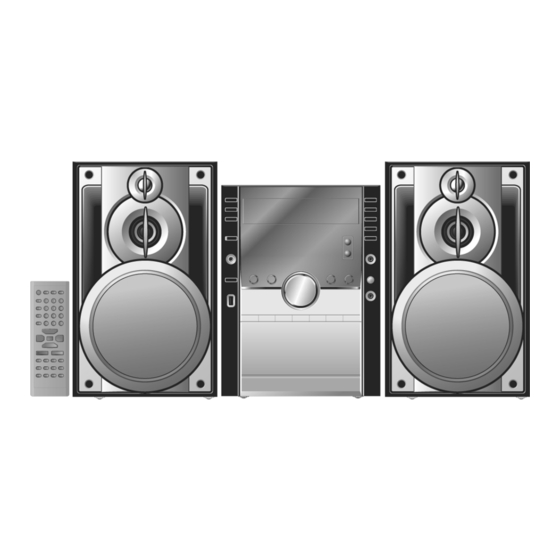
SA-AK450GCP
Colour
(K)... Black Type
Audio performance (Amplifier)
Input sensitivity/Input impedance
Aux
Music Port input jack
Terminal
Sensitivity
Phone jack
Terminal
MIC jack
Terminal
Sensitivity
n CASSETTE DECK SECTION
Track system
Heads
Record/playback
Erasure
Motor
Recording system
Erase system
Tape speed
Overall frequency response (+3, -6 dB) at DECK OUT
NORMAL
© 2007 Matsushita Electric Industrial Co. Ltd.. All
rights
reserved.
distribution is a violation of law.
ORDER NO. MD0703009CE
CD Stereo System
250mV, 14.7 kΩ
Stereo, 3.5 mm jack
100 mV, 4.7 kΩ
Stereo, 3.5 mm jack
Mono, 3.5 mm jack
0.7 mV, 680 Ω
4 track, 2 channel
Solid permalloy head
Double gap ferrite head
DC servo motor
AC bias 100 kHz
AC erase 100 kHz
35 Hz to 14 kHz
Unauthorized
copying
4.8 cm/s
and
Advertisement
Table of Contents

Related Manuals for Panasonic SA-AK450GCP


Summary of Contents for Panasonic SA-AK450GCP
-
Page 1: Specifications
ORDER NO. MD0703009CE CD Stereo System SA-AK450GCP Colour (K)... Black Type Notes: This model’s CD mechanism changer unit is CRS1. Please refer to the original Service Manual (Order No. MD0509368C0) for this mechanism. Specifications n AMPLIFIER SECTION Audio performance (Amplifier) -
Page 2: Table Of Contents
SA-AK450GCP S/N Ratio 50 dB (A weighted) USB memory port Wow and flutter 0.18 % (WRMS) Maximum current 500 mA Fast forward and rewind time Approx. 120 seconds with Bit rate C-60 cassette tape 32 kbps to 320 kbps n DISC SECTION... - Page 3 SA-AK450GCP 10.4. Disassembly of Top Cabinet 16 Wiring Connection Diagram 10.5. Disassembly of CD Changer Unit (CRS1) 17 Block Diagram 10.6. Disassembly of Rear Panel 17.1. CD Servo Diagram 10.7. Disassembly of Main P.C.B. 17.2. Deck/ Deck Mechanism Diagram 10.8. Disassembly of Transformer P.C.B.
-
Page 4: Safety Precautions
SA-AK450GCP 1 Safety Precautions 1.1. General Guidelines 1. When servicing, observe the original lead dress. If a short circuit is found, replace all parts which have been overheated or damaged by the short circuit. 2. After servicing, ensure that all the protective devices such as insulation barriers and insulation papers shields are properly installed. -
Page 5: Safety Part Information
SA-AK450GCP · No sound is heard when the power is turned on. · Sound stops during a performance. The function of this circuitry is to prevent circuitry damage if, for example, the positive and negative speaker connection wires are “shorted”, or if speaker systems with an impedance less than the indicated rated impedance of the amplifier are used. - Page 6 SA-AK450GCP together of your clothes fabric or the lifting of your foot from a carpeted floor can generate static electricity (ESD) sufficient to damage an ES device).
-
Page 7: Handling Precautions For Traverse Deck
SA-AK450GCP 3 Handling Precautions For Traverse Deck The laser diode in the traverse deck (optical pickup) may break down due to potential difference caused by the static electricity of clothes or our human body. So, be careful of electrostatic breakdown during repair of the traverse deck (optical pickup). - Page 8 SA-AK450GCP...
-
Page 9: Precaution Of Laser Diode
SA-AK450GCP 4 Precaution of Laser Diode Caution : This product utilizes a laser diode with the unit turned "ON", invisible laser radiation is emitted from the pick up lens. Wavelength : 785 nm(CD)/662 nm(DVD) Maximum output radiation power from pick up : 100 µW/VDE Laser radiation from pick up unit is safety level, but be sure the followings: 1. -
Page 10: Warning
SA-AK450GCP 5 Warning 5.1. Service caution based on legal restrictions 5.1.1. General description about Lead Free Solder (PbF) The lead free solder has been used in the mounting process of all electrical components on the printed circuit boards used for this equipment in considering the globally environmental conservation. -
Page 11: Accessories
SA-AK450GCP 6 Accessories Remote Control FM Antenna Wire AC Cord AM Loop Antenna AC Plug Adapter... -
Page 12: Operating Procedures
SA-AK450GCP 7 Operating Procedures 7.1. Main Unit Key Buttons Operations... -
Page 13: Remote Control Key Buttons Operations
SA-AK450GCP 7.2. Remote Control Key Buttons Operations... -
Page 14: New Features
SA-AK450GCP 8 New Features 8.1. Using the Music Port and USB Mass Storage Class Device This feature enables you to enjoy music from a portable audio equipment. - Page 15 SA-AK450GCP With reference to page 15 of the operating instruction manual. With reference to page 16 of the operating instruction manual.
-
Page 16: Self Diagnosis And Special Mode Setting
SA-AK450GCP 9 Self diagnosis and special mode setting This unit is equipped with functions for checking and inspecting namely: Self-Diagnostic and Test Mode. 9.1. Service Mode Summary Table The service modes can be activated by pressing various button combination on the main unit and remote control unit. Below is the... - Page 17 SA-AK450GCP Item FL Display Key Operation Mode Name Description Front Key Doctor Mode To enter into Doctor (Display 1) In any mode: Mode for checking of 1. Press [ ] button on main unit various items and follow by [4] and [7] on remote control.
- Page 18 SA-AK450GCP Item FL Display Key Operation Mode Name Description Front Key Tape Eject Test To check on the tape In doctor mode: eject function (For deck 1. Press [0] button on remote control. 1/2) FL Display Test To check In doctor mode:...
-
Page 19: Reliability Test Mode (Crs1 Mechanism)
SA-AK450GCP Note: Microprocessor firmware refers to version number for microprocessor IC located on PANEL P.C.B.. It is subject to change which would be updated accordingly. ROM correction checksum refers to the HEX code that is displayed upon key buttons pressed if an EEPROM is loaded in the unit. -
Page 20: Error Code Table Display
SA-AK450GCP 9.4. Error code Table Display Self-Diagnosis Function (refer Section 9.2) provides information on any problems occuring for the unit and its respective components by displaying the error codes. These error code such as U**, H** and F** are stored in memory and held unless it is... - Page 21 SA-AK450GCP The error code is automatically display after entering into self-diagnostic mode. 9.4.1. Error Code Table for Deck Mechanism Error Code Diagnosis Contents Description of error Automatic FL Display Remarks Mode SW, plunger Normal operation during For deck mechanism unit.
- Page 22 SA-AK450GCP Error Code Diagnosis Contents Description of error Automatic FL Display Remarks HOME Cam gear/gear Cam gear does not move to For CD changer unit (CRS1). Press [SINGLE CHANGE] on main assembly abnormal “HOME” position under following conditions unit for next error.
- Page 23 SA-AK450GCP · Only the first 5 errors will be memorized (in backup memory). The subsequence error shall be ignored and not memorize. For system with EEPROM as memory backup,memory space in EEPROM is neccesary. 2. To display all error code memorized In CRS1 Self-Diagnostic mode, press [SINGLE CHANGE] to display subsequence error code.
-
Page 24: Assembling And Disassembling
SA-AK450GCP 10 Assembling and Disassembling 10.1. Caution Special Note: This model uses a new CD changer unit CRS1. In this following section does not contain the necessary disassembly & assembly information for the CD changer unit (CRS1) except the disasembly & assembly of traverse unit. Kindly refer to the original service manual for the CD changer unit. -
Page 25: Disassembly Flow Chart
SA-AK450GCP 10.2. Disassembly flow chart The following chart is the procedure for disassembling the casing and inside parts for internal inspection when carrying out the servicing. To assemble the unit, reverse the steps shown in the chart as below. -
Page 26: Main Parts Location
SA-AK450GCP 10.3. Main Parts Location... -
Page 27: Disassembly Of Top Cabinet
SA-AK450GCP 10.4. Disassembly of Top Cabinet Step 1 Remove 3 screws on both sides on top cabinet. Step 2 Remove 5 screws at the rear. Step 3 Lift the sides of top cabinet outwards. Step 4 Push the top cabinet backwards to release catches. -
Page 28: Disassembly Of Rear Panel
SA-AK450GCP Step 4 Lift the CD changer unit upwards to remove it. · Disassembly of Mecha Chassis Step 5 Remove 2 screws. Step 6 Remove the Mecha Chassis. Note: For disassembly & assembly of traverse unit, please refer to section 10.16 of this service manual.Please refer to original Service Manual for the Disassembly and Assembly of the CD Changer Unit (CRS1). - Page 29 SA-AK450GCP Step 2 Detach cable CN2810 at Main P.C.B.. Step 3 Detach FFC cables (CN2801 & CN2805) at Main P.C.B.. Step 4 Remove rear panel.
-
Page 30: Disassembly Of Main P.c.b
SA-AK450GCP 10.7. Disassembly of Main P.C.B. · Follow the (Step 1) - (Step 5) of Item 10.4 · Follow the (Step 1) - (Step 4) of Item 10.5 · Follow the (Step 1) - (Step 4) of Item 10.6 Step 1 Detach FFC cables (CN2803, CN2806 & CN3200) at Main P.C.B.. -
Page 31: Disassembly Of Power P.c.b
SA-AK450GCP 10.9. Disassembly of Power P.C.B. · Follow the (Step 1) - (Step 5) of Item 10.4 · Follow the (Step 1) - (Step 4) of Item 10.5 · Follow the (Step 1) - (Step 4) of Item 10.6 · Follow the (Step 1) - (Step 3) of Item 10.7 Step 1 Remove the 5 screws on Power P.C.B.. -
Page 32: Disassembly Of Front Panel Unit
SA-AK450GCP Step 3 Remove up the heat sink sub assembly (with IC5501). Step 4 Remove screw and IC clip. Step 5 Remove IC5501 from the sub assembly. Caution: During assembly of the heat sink sub assembly (with IC5501) all soldering points is touch-up to avoid dry- joints. -
Page 33: Disassembly For Panel P.c.b
SA-AK450GCP Step 5 Remove the front panel unit. Note: Ensure 2 claws located at the bottom chassis is seated into the 2 slots at bottom of front panel at 2 catches (one on each side) of bottom chassis to be aligned to front panel’s slot. -
Page 34: Disassembly Of Tact Switch P.c.b
SA-AK450GCP Step 2 Remove Lid. Note: Do not misplace the spring. 10.12. Disassembly of Tact Switch P.C.B. · Follow the (Step 1) - (Step 5) of Item 10.4 · Follow the (Step 1) - (Step 4) of Item 10.5 · Follow the (Step 1) - (Step 5) of Item 10.10 Step 1 Remove 4 screws at Tact Switch P.C.B.. -
Page 35: Disassembly Of Deck Mechanism Unit
SA-AK450GCP Step 4 Unsolder 4 points. Step 5 Remove USB P.C.B.. 10.14. Disassembly of Deck mechanism unit · Follow the (Step 1) - (Step 5) of Item 10.4 · Follow the (Step 1) - (Step 4) of Item 10.5 · Follow the (Step 1) - (Step 5) of Item 10.10 Step 1 Remove the 4 screws. -
Page 36: Disassembly Of Traverse Unit
SA-AK450GCP Step 3 Remove Deck P.C.B. Step 2 Desolder wire at deck motor terminals. 10.16. Disassembly of Traverse Unit · Follow the (Step 1) - (Step 5) of Item 10.4 · Follow the (Step 1) - (Step 4) of Item 10.5 Important notes: Ensure all the trays are in the “STOCK”... -
Page 37: Disassembly For Deck Mechanism
SA-AK450GCP Step 3: Remove the traverse unit as arrow shown. · Assembly of Traverse Unit Step 2: Push the traverse slide plate as arrow shown to lock the traverse unit. Step 1: Turn over the unit and install the traverse unit. - Page 38 SA-AK450GCP 10.17.1. Replacement of Pinch Roller and Head Block...
- Page 39 SA-AK450GCP 10.17.2. Replacement of Motor, Capstan Belt A, Capstan Belt B, and Winding Belt...
-
Page 40: Disassembly Of Deck Mechanism P.c.b
SA-AK450GCP 10.18. Disassembly of Deck Mechanism P.C.B. · Follow the (Step 1) - (Step 4) of Item 10.4 · Follow the (Step 1) - (Step 4) of Item 10.5 · Follow the (Step 1) - (Step 5) of Item 10.10 ·... -
Page 41: Disassembly Of Cassette Lid
SA-AK450GCP 10.19. Disassembly of cassette lid · Follow the (Step 1) - (Step 4) of Item 10.4 · Follow the (Step 1) - (Step 4) of Item 10.5 · Follow the (Step 1) - (Step 5) of Item 10.10 · Follow the (Step 1) - (Step 3) of Item 10.14 Step 1 Lift up the lever upward, open the cassette deck. - Page 42 SA-AK450GCP Step 2 Push the lever upward and open the cassette lid. Remove the cassette tape. Note: Follow 10.19 Disassembly of cassette lid (Step1) to (Step 3). Remove the cassette tape.
-
Page 43: Service Fixture And Tools
SA-AK450GCP 11 Service Fixture and Tools Service Tools Extension FFC (A) Deck P.C.B. - Main P.C.B. REEX0485 (14 Pins) 12 Service Positions Note: For description of the disassembly procedures, see the Section 10. 12.1. Checking and Repairing of Main P.C.B. -
Page 44: Checking And Repairing Of Transformer P.c.b
SA-AK450GCP 12.2. Checking and Repairing of Transformer P.C.B. 12.3. Checking and Repairing of Panel, Deck & Deck Mechanism P.C.B. -
Page 45: Checking And Repairing Of Power P.c.b
SA-AK450GCP 12.4. Checking and Repairing of Power P.C.B. -
Page 46: Procedure For Checking Operation Of Individual Parts Of Deck Mechanism Unit
SA-AK450GCP 13 Procedure for Checking Operation of Individual Parts of Deck Mechanism Unit 13.1. Operation Check with Cassette Tape 1. Pull up the EJECT lever using a rubber band. (Fig. 6) 2. Supply DC5V to MOTOR. (→ MOTOR rotates.) (Fig. 5) 3. - Page 47 SA-AK450GCP...
-
Page 48: Measurement And Adjustments
SA-AK450GCP 14 Measurement And Adjustments 14.1. Cassette Deck Section 14.1.1. Requirements · Test tape (QZZCFM) (QZZCWAT) · Normal blank cassette tape (QZZCRA) · Digital frequency counter · Oscilloscope · Electrical voltmeter · Headphone jack output jig (Fig 8) 14.1.2. Setting of Unit ·... - Page 49 SA-AK450GCP Fig. 10 Fig. 11 14.1.5. Bias Voltage Check 1. Connect an electrical voltmeter. (Fig 12) (Fig 9 for location of test points) 2. Set the function to “TAPE” position. 3. Insert a normal blank cassette tape (QZZCRA). 4. While pressing and holding down [REC( )] button, press [TAPE( )] button to pause the recording mode.
-
Page 50: Voltage And Waveform Chart
SA-AK450GCP 15 Voltage and Waveform Chart Note: Circuit voltage and waveform described herein shall be regarded as reference information when probing defect point, because it may differ from an actual measuring value due to difference of Measuring instrument and its measuring condition and product itself. -
Page 51: Main P.c.b
SA-AK450GCP 15.2. Main P.C.B. 15.3. Panel P.C.B. -
Page 52: Power P.c.b. & Transformer P.c.b
SA-AK450GCP 15.4. Power P.C.B. & Transformer P.C.B. 15.5. CD Servo P.C.B. -
Page 53: Waveform Chart
SA-AK450GCP 15.6. Waveform Chart... -
Page 54: Wiring Connection Diagram
SA-AK450GCP 16 Wiring Connection Diagram JK2803 9 ..1 CN3601 H5104 CN2810 TUNER MOTOR PACK CN2809 POWER P.C.B. SOLDER SIDE CN2801 MAIN P.C.B. SOLDER SIDE RIGHT SPEAKERS TO CRS1 JK5101 CN3200 (CN1) LEFT SPEAKERS CN2808 CN2805 CN5103 1 . -
Page 55: Block Diagram
SWITCH PROCESSOR/ TO MAIN CN7002 CN2801 (1/2) DIGITAL FILTER 3.3V 3.3V 3.3V 3.3V D/A CONVERTER MUTE PC1 4 CN7002 CN2801 [CH1] LCH OUT 3.3V TO MAIN CN7002 CN2801 (2/2) RCH OUT MUTE PC2 2 [CH2] SA-AK450GCP CD SERVO BLOCK DIAGRAM... -
Page 56: Deck/ Deck Mechanism Diagram
: CD SIGNAL LINE : CD-DA (AUDIO/VIDEO) SIGNAL LINE : MAIN SIGNAL LINE : AM SIGNAL LINE : FM/AM/XM SIGNAL LINE : FM SIGNAL LINE : AUX/IPOD SIGNAL LINE ( ) Indicates the Pin No. of Right Channel. SA-AK450GCP DECK/DECK MECHANISM BLOCK DIAGRAM... -
Page 57: Main Diagram
FROM DECK Q2501 D2503 LM.1 LEVEL METER CONTROL SWITCH ASPDA ASPCLK IDCDET Q2942 FAN MOTOR ON/OFF SWITCH TO FAN D2947 Q2943 FAN SUPPLY FROM POWER CONTROL SWITCH Q2949 Q2948 D2946 DC DETECT DC DETECT SWITCH SWITCH SA-AK450GCP MAIN 1/2 DIAGRAM... - Page 58 CONTROLSWITCH QR3105 QR3106 Q2803 SWITCH SWITCH IC4000 C0DBZGC00067 RESET (MICRO-P) 3.3 REGULATOR SWITCH Q3601 STBY SWITCH Q2950 D2936 DECK SUPPLY DVREF CONTROL SWITCH IC2872 C0CBAHG00011 VOLTAGE Q2950 REGULATOR DECK SUPPLY CONTROL SWITCH 3.3V D2811 D2813 D3400 SA-AK450GCP MAIN 2/2 DIAGRAM...
-
Page 59: Panel Diagram
Q6502 VR6511 VOLUME TO MAIN (1/2) JK6751 M.PORT S6201-S6207 TO MAIN (2/2) JK6551 HEADPHONE TO MAIN (1/2) SUB PANEL CIRCUIT S6301-S6309 VR6491 +VREF MIC VOLUME +VREF TO MAIN (2/2) S6106-S6108 S6101-S6105 QR6457 MOT10V DRIVE SUB PANEL P.C.B SA-AK450GCP PANEL DIAGRAM... -
Page 60: Power Diagram
FAN ON/OFF SWITCH SWITCH D5126 TO MAIN (1/2) Q5111 Q5101,Q5110 +15V REGULATOR Q5102 Q5108,Q5109 CURRENT CONTROL SWITCH TO TRANSFORMER Q5112,Q5114 Q5113 CURRENT STABLISER CURRENT LMIITER 11V REGULATOR SWITCH IC5101 TO MAIN C0DAZYY00005 (2/2) REGULATOR IC D5130 5.6V 3.3V SA-AK450GCP POWER DIAGRAM CTRL... -
Page 61: Usb/ Transformer Diagram
STCLK 59 6 USBD+ CD_DATA 58 CD_STAT 57 Q5953 RL5950 CD_CLK 56 PCONT SWITCH TO PANEL I2C_REQ/WR_START Q5952 T5951 VERR 50 SYNCHRONISATION SWITCH D5966 JK5950 L5950 Z5950 D5951, Q5950 Q5950 D5952 D5963 CURRENT VOLTAGE LIMITING REGULATOR SWITCH SA-AK450GCP USB/TRANSFORMER DIAGRAM... - Page 62 SA-AK450GCP...
-
Page 63: Notes Of Schematic Diagram
SA-AK450GCP 18 Notes Of Schematic Diagram (All schematic diagrams may be modified at any time with : CD Signal line the development of new technology) : Main Signal line Notes: S971: Mode switch. : FM/AM Signal line S972: Half switch. - Page 64 SA-AK450GCP...
-
Page 65: A) Cd Servo Circuit
12 11 R7220 R7330 W7002 W7004 5.6K C7335 IC7002 X7201 C7315 H2B169500005 0.47 BA5948FPE2 C7334 4 CH DRIVE IC C7338 10V220 0.056 R7331 R7323 3.3k R7315 R7325 3.3k R7332 R7335 M7301 M7302 TRAVERSE MOTOR SPINDLE MOTOR SA-AK450GCP CD SERVO CIRCUIT... -
Page 66: B) Main Circuit
SA-AK450GCP 19.2. (B) Main Circuit SCHEMATIC DIAGRAM - 2 MAIN CIRCUIT : TAPE PLAYBACK SIGNAL LINE : FM/AM SIGNAL LINE : MAIN SIGNAL LINE : AUX SIGNAL LINE : MIC SIGNAL LINE : +B SIGNAL LINE : CD SIGNAL : TAPE RECORD SIGNAL LINE... -
Page 67: Main Circuit
SUBW C3709 W586 K3705 R2456 R3711 180k +15V R2417 C3707 R2423 C2423 R2428 C3710 R2418 0.015 R2429 R2426 100k 0.1u R3709 3.3K R3712 Q2417 R2416 W654 2.2k C2421 R2421 C2425 16V10 C2943 50V2.2 TO MAIN SECTION (4/4) SA-AK450GCP MAIN CIRCUIT... - Page 68 SA-AK450GCP SCHEMATIC DIAGRAM - 4 MAIN CIRCUIT : +B SIGNAL LINE : CD SIGNAL LINE : FM/AM SIGNAL LINE : MAIN SIGNAL LINE : AUX SIGNAL LINE : USB SIGNAL LINE W658 D2811 B0ADCJ000020 R2894 R2121 3.3k TO MAIN SECTION (1/4) C2121 +3.3V...
- Page 69 W615 Q2937 Q2936 28 27 25 24 21 20 12 11 11 12 13 14 B1ACKD000006 CD SUPPLY CONTROL SWITCH Q2937 B1GBCFJJ0051 CHANGER PLUNGER CN2806 CN2805 ON/OFF SWITCH TO CRSI (CN1) PANEL CIRCUIT (CN6601) IN SCHEMATIC DIAGRAM-6 SA-AK450GCP MAIN CIRCUIT...
-
Page 70: C) Panel Circuit
C6502 R6753 W901 Q6501 L6501 C6510 C6504 R6751 3.3K 3.3K MUSIC PORT L6502 C6509 R6509 W910 C6753 C6751 C6503 0.01 0.01 R6503 0.047 C6506 R6506 C6505 0.01 W1004 2.2K 0.22 W1000 JK6501 JK6751 VR6511 EVUF2AF15B14 MIC VOLUME SA-AK450GCP PANEL CIRCUIT... -
Page 71: D) Sub Panel Circuit & (G) Deck Mechanism Circuit
S6305 R6306 2.2K R6491 R6107 S6306 R6307 2.7K S6108 2.7K M.EQ+ C6492 C6491 100P 100P HARD R6108 BASS S6307 4.7K R6308 R6310 MANUAL 4.7K S6308 COM B R6309 6.8K M.EQ- S6309 VR6491 EVEKE2F3024B VOLUME JOG SA-AK450GCP SUB PANEL/DECK MECHANISM CIRCUIT... -
Page 72: E) Power Circuit
100P IC5201 Q5202 100P Q5201 Q5103,Q5104 X5202 B1ADCF000063 B1ABCF000176 FREQUENCY HOPPING R5207 FAN ON/OFF SWITCH SWITCH 6.8K Q5104 Q5202 Q5103 X5201 H2A415300001 R5209 C5204 100P AGND C5205 C5208 X5202 6.3V220u 0.1u H2A375300003 AGND D5126 R5150 B0ACCK000005 220K SA-AK450GCP POWER CIRCUIT... - Page 73 R5105 IN SCHEMATIC R5110 MUTE_F 2.2K mUTE-F_HOP C5133 DIAGRAM-5 MOTOR12V 6.3V100 D5103 C5113 MOTOR 12V B0BA5R100004 50V33 D5109 XM5.3V R5132 XM5.3V B0BA01100004 -9V AGND AGND Q5109 Q5114 +3.3V 2SB0709AHL CN5103 B1ABCF000176 VOLTAGE REGULATOR 11V REGULATOR E5103 K9ZZ00001279 SA-AK450GCP POWER CIRCUIT...
-
Page 74: F) Deck Circuit
R1337 R1332 B0ACCK000005 MOTOR_GND MOTOR_H C1311 C1320 16V47 50V1 R1331 DECK MECHANISM (CS971) Q1315 CN1305 7.5K ON SCHEMATIC DIAGRAM-7 Q1314 R1344 R1342 R1341 R1374 R1343 3.3K Q1316 WR1903 R1345 2SD09650RA SWITCH Q1314 Q1315 B1GDCFGH0002 B1ACKD000006 SWITCH SWITCH SA-AK450GCP DECK CIRCUIT... -
Page 75: H) Transformer Circuit
C5964 R5954 PCONT SWITCH 0.01u 820K C5951 JK5950 0.01u C5953 AC IN 0.01u 110V-127V/220V-240V R5952 Z5950 250V T4AL 4.7K ERZV10V511CS 50Hz/60Hz D5969 B0AAFK000004 R5958 C5963 50V4.7 Q5952 B1GACFJJ0018 C5962 C5952 SYNCHRONISATION SWITCH 16V220 C5954 R5957 10V47 0.01 SA-AK450GCP TRANSFORMER CIRCUIT... -
Page 76: I) Usb Circuit
LB938 MAIN CIRCUIT CD_DATA (CN3200) IN DGND SCHEMATIC J0JAC0000021 LB840 STCLK DIAGRAM-4 TERR J0JAC0000021 LB841 STREQ J0JAC0000021 LB843 STIN J0JAC0000021 LB845 CD_MLD J0JAC0000021 LB846 CD_NRST J0JAC0000021 LB848 M_NRST DGND J0JHC0000045 LB850 LB852 D3.3V DGND J0JHC0000045 MMOD P901 SA-AK450GCP USB CIRCUIT... -
Page 77: Printed Circuit Board
SA-AK450GCP 20 Printed Circuit Board Note: Circuit board diagrams may be modified at any time with the development of new technology. - Page 78 SA-AK450GCP 20.1. (A) CD Servo P.C.B., (F) Deck P.C.B. & (G) Deck Mechanism P.C.B. CD SERVO P.C.B (REPV0111A) DECK P.C.B (REPV0134B) (RF) TP51 C7227 W1930 TP19 W7014 Q1309 CN1305 Q1310 TP14 C7204 W7015 W1909 W1935 C7226 R7212 TP18 TP50 C7228...
-
Page 79: B) Main P.c.b
SA-AK450GCP 20.2. (B) Main P.C.B. MAIN P.C.B (REPV0130H) AUX IN W565 W574 L2996 R2447 C2705 R2702 R2941 W566 W573 R2446 W570 C2941 C2312 C2240 Q2441 R2145 W572 R2705 R2703 W277 R2241 C2983 W567 W569 R2944 C2981 R2315 C2703 C2944 C2441... -
Page 80: C) Panel P.c.b
SA-AK450GCP 20.3. (C) Panel P.C.B. PANEL P.C.B (REPV0131E) S6103 S6201 (CD1) (OPEN/CLOSE) R6481 QR6461 R6202 R6105 R6760 S6202 S6102 (CD2) R6759 (MULTI CHANGE) QR6462 W807 R6632 W808 W809 S6203 R6758 R6102 (CD3) J6553 R6756 W909 S6104 J6551 (SINGLE CHANGE) R6755... -
Page 81: D) Sub Panel P.c.b. & (I) Usb P.c.b. (Side A & B)
SA-AK450GCP 20.4. (D) Sub Panel P.C.B. & (I) USB P.C.B. (Side A & B) SUB PANEL P.C.B (REPV0131E) USB P.C.B (REPV0101A) JW6001 D6462 (VOL. LED) S6304 S6305 R6302 R6303 (TUNER/FM/AM) (EXT_IN) D 6 4 6 1 R6457 VR6491 R6304 S6302... -
Page 82: E) Power P.c.b. 20.6. (H) Transformer P.c.b
SA-AK450GCP 20.5. (E) Power P.C.B. POWER P.C.B (REPV0133B) H5104 W701 C5171 W602 C5102 W716 C5103 C5172 R5203 W662 W697 R5201 W698 R5202 Q5202 C5204 W700 C5203 W691 C5202 W737 W638 R5207 Q5201 C5301 C5302 R5522 C5332 C5330 R5206 W639 R5302... -
Page 83: H) Transformer P.c.b
SA-AK450GCP 20.6. (H) Transformer P.C.B. TRANSFORMER P.C.B (REPV0132E) T5951 250V T4AL R5954 (SUB TRANSFORMER) Q5954 D5968 C5953 Q5950 J5955 R5952 Z5950 C5951 C5952 D5952 RL5950 C5954 250V T2AL JK5950 Q5952 W5914 Q5953 W5915 CN5951 R5958 AC IN ~ W5905 R5951... - Page 84 SA-AK450GCP...
-
Page 85: Illustration Of Ics, Transistors And Diodes
SA-AK450GCP 21 Illustration of ICs, Transistors and Diodes C0AABB000125 C0ABBB000244 (8P) C0CBAHG00011 C1AA00000612 C1BB00001121 (100P) MN6627954MA (100P) C2CBYY000423 (100P) C0HBB0000057 (44P) MNZSFB5KJM1 (64P) C0DAZYY00005 C0JBAB000011(14P) AN7326K (26P) C0DBZGC00067 BA5948FPE2 C0GAG0000007 C1BA00000487 (24P) CNB13030R2AU C3EBEG000072 (8P) B1AAKD000014 2SD09650RA B1GACFJJ0018 B1DEGM000026 B1ACKD000006... -
Page 86: Terminal Function Of Ic's
SA-AK450GCP 22 Terminal Function of IC's 22.1. IC7001 (MN6627954MA) Servo Processor,Digital Signal Processor/Digital filter and D/A Converter Pin No. Mark Function Pin No. Mark Function DRAM address signal O/P 11 DSLF Loop Filter Terminal (For DSL) DRAM address signal O/P 9... -
Page 87: Ic7002 (Ba5948Fpe2) Ic 4Ch Drive
SA-AK450GCP 22.2. IC7002 (BA5948FPE2) IC 4CH Drive Pin No. Mark Function Pin No. Mark Function Motor Driver 92 Input Motor Drive (3) reverse - action output Turntable Motor Drive Signal (“L”:ON) Motor Drive (3) forward - action output Motor Drive (1) Input... - Page 88 SA-AK450GCP Pin No. Mark Function /Reset_SW CD Limit Switch Input for the most Inner Point (Active Low) HOME_SW Home Switch for CRS1 CD_RST CD Reset output CLOSE_SW CLOSE switch for CRS1 OPEN_SW Open switch for CRS1 CRS1 motor CW CRS1 motor CCW...
-
Page 89: Exploded Views
SA-AK450GCP 23 Exploded Views 23.1. Cabinet Parts Location... - Page 90 SA-AK450GCP...
-
Page 91: Deck Mechanism Parts Location (Raa4403-S)
SA-AK450GCP 23.2. Deck Mechanism Parts Location (RAA4403-S) -
Page 92: Packaging
SA-AK450GCP 23.3. Packaging... -
Page 93: Replacement Parts List
SA-AK450GCP 24 Replacement Parts List Notes: · Important safety notice: Components identified by mark have special characteristics important for safety. Furthermore, special parts which have purposes of fire-retardent (resistors), high-quality sound (capacitors), low noise (resistors), etc are used. When replacing any of these components, be sure to use only manufacturer’s specified parts shown in the parts list. - Page 94 SA-AK450GCP Ref. No. Part No. Part Name & Description Remarks Ref. No. Part No. Part Name & Description Remarks RXQ0470-2 PLUNGER ASS’Y Q2142 B1ABCF000176 TRANSISTOR RMC0061 PACK SPRING Q2242 B1ABCF000176 TRANSISTOR RXF0061-1 FLYWHEEL F ASS’Y Q2311 B1ABGC000005 TRANSISTOR RXG0040 FF RELAY GEAR ASS’Y...
- Page 95 SA-AK450GCP Ref. No. Part No. Part Name & Description Remarks Ref. No. Part No. Part Name & Description Remarks D5107 B0BA01500003 DIODE S6303 EVQ21405RJ SW TAPE D5109 B0BA01100004 DIODE S6304 EVQ21405RJ SW TUNER/FM/AM D5121 B0EAKP000134 DIODE S6305 EVQ21405RJ SW EXT IN...
- Page 96 SA-AK450GCP Ref. No. Part No. Part Name & Description Remarks Ref. No. Part No. Part Name & Description Remarks LB951 J0JHC0000045 CHIP INDUCTOR W580 ERJ3GEY0R00V CHIP JUMPER LB952 J0JHC0000045 CHIP INDUCTOR W581 ERJ3GEY0R00V CHIP JUMPER LB7262 D0GBR00JA008 CHIP JUMPER W582...
- Page 97 SA-AK450GCP Ref. No. Part No. Part Name & Description Remarks Ref. No. Part No. Part Name & Description Remarks W655 ERJ6GEY0R00V CHIP JUMPER W7013 D0GBR00JA008 CHIP JUMPER W656 ERJ6GEY0R00V CHIP JUMPER W7014 D0GBR00JA008 CHIP JUMPER W657 ERJ6GEY0R00V CHIP JUMPER W7015...
- Page 98 SA-AK450GCP Ref. No. Part No. Part Name & Description Remarks Ref. No. Part No. Part Name & Description Remarks R1203 D0GB183JA008 18K 1/16W R2245 D0GB102JA008 1K 1/16W R1204 D0GB103JA008 10K 1/16W R2246 D0GB102JA008 1K 1/16W R1205 D0GB222JA007 2.2K 1/16W R2247...
- Page 99 SA-AK450GCP Ref. No. Part No. Part Name & Description Remarks Ref. No. Part No. Part Name & Description Remarks R2507 D0GB104JA007 100K 1/16W R2924 D0GB102JA008 1K 1/16W R2508 D0GB102JA008 1K 1/16W R2927 D0GB102JA008 1K 1/16W R2509 D0GB561JA007 560 1/16W R2936...
- Page 100 SA-AK450GCP Ref. No. Part No. Part Name & Description Remarks Ref. No. Part No. Part Name & Description Remarks R5201 D0GB102JA008 1K 1/16W R6481 ERJ3GEY0R00V 0 1/16W R5202 D0GB104JA007 100K 1/16W R6491 D0GB223JA041 22K 1/16W R5203 D0GB103JA008 10K 1/16W R6492...
- Page 101 SA-AK450GCP Ref. No. Part No. Part Name & Description Remarks Ref. No. Part No. Part Name & Description Remarks C908 F1G1H220A565 22P 50V C2182 F1H1A105A025 1 10V C911 F1G1C104A083 0.1 16V C2183 ECJ1VB1C224K 0.22 16V C912 F1G1C104A083 0.1 16V C2191 F2A1H4R7A234 4.7 50V...
- Page 102 SA-AK450GCP Ref. No. Part No. Part Name & Description Remarks Ref. No. Part No. Part Name & Description Remarks C2701 F1H1H103A219 0.01 50V C5157 F1H1H103A219 0.01 50V C2702 F2A1C101A234 100 16V C5159 F1H1H103A219 0.01 50V C2703 F1H1H471A219 470P 50V C5171...
- Page 103 SA-AK450GCP Ref. No. Part No. Part Name & Description Remarks Ref. No. Part No. Part Name & Description Remarks C5425 ECJ1VB1H104K 0.1 50V C7217 ECJ1VB1C104K 0.1 16V C5426 ERJ3GEY0R00V 0 1/16W C7218 ECJ1VB1C823K 0.082 16V C5427 ECQV1H474JL3 0.47 50V C7223 F2A1H4R70037 4.7 50V...