Table of Contents
Advertisement
Quick Links
Advertisement
Table of Contents

Related Manuals for Panasonic KX-T7603X


Summary of Contents for Panasonic KX-T7603X
- Page 1 ORDER NO. KMS0303669C8 Add on Key Module KX-T7603X (for Asia, MiddleNear East, Africa, Oceania, Latin America, Russia, Europe) 2003 Panasonic Communications Co., Ltd. All rights reserved. Unauthorized copying and distribution is a violation of law.
-
Page 2: About Lead Free Solder (Pbf: Pb Free)
IMPORTANT INFORMATION ABOUT LEAD FREE, (PbF), SOLDERING If lead free solder was used in the manufacture of this product the printed circuit boards will be marked PbF. Standard leaded, (Pb), solder can be used as usual on boards without the PbF mark. When this mark does appear please read and follow the special instructions described in this manual on the use of PbF and how it might be permissible to use Pb solder during service and repair work. -
Page 3: For Service Technicians
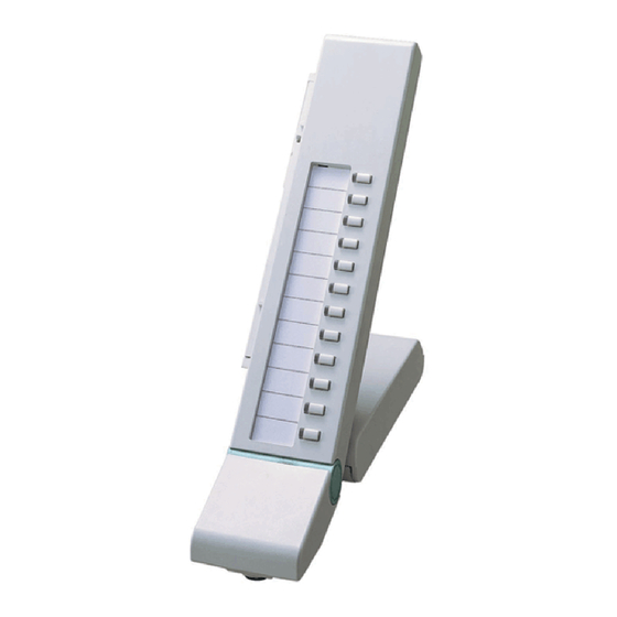
1.1. SUGGESTED PbF SOLDER There are several types of PbF solder available commercially. While this product is manufactured using Tin, Silver, and Copper, (Sn+Ag+Cu), you can also use Tin and Copper, (Sn+Cu), or Tin, Zinc, and Bismuth, (Sn+Zn+Bi). Please check the manufac turer’s specific instructions for the melting points of their products and any precautions for using their product with other materials. - Page 4 Jacks: TEL Jack Dimensions: 255 (D)mm [Operate] × 47 (W)mm × 94 (H)mm Angle: 206 (D)mm [Operate] × 47 (W)mm × 178 (H)mm High 213 (D)mm [Base] Angle: Weight: 210g Design and specifications are subject to change without notice. 4. INSTALLING For KX-T7633 / KX-T7636 The Add-on Key Module has 12 CO buttons.
- Page 5 Open the cover. Attach the KX-T7603 to your telephone with screws. Insert the flat cable into the connector.
- Page 6 Close the cover. 5. DISASSEMBLY INSTRUCTIONS 1. Remove Two Screws (A). 2. Remove the Connect Plate. 3. Remove Screw (A). 4. Remove the Bottom Cabinet and Top Cabinet (Base).
-
Page 7: How To Replace A Flat Package Ic
5. Remove Two Screws (A). 6. Remove the Bottom Cabinet (Oper). 7. Remove the Main Board from the Top Cabinet. 6. HOW TO REPLACE A FLAT PACKAGE IC 6.1. PREPARATION - PbF (: Pb free) Solder - Soldering Iron Tip Temperature of 700°F ± 20°F (370°C ± 10°C) Note: We recommend a 30 to 40 Watt soldering iron. - Page 8 6.2. PROCEDURE 1. Tack the flat pack IC to the PCB by temporarily soldering two diagonally opposite pins in the correct positions on the PCB. Be certain each pin is located over the correct pad on the PCB. 2. Apply flux to all of the pins on the IC. 3.
-
Page 9: Troubleshooting Guide
7. TROUBLESHOOTING GUIDE CROSS REFERENCE: WAVEFORM 8. BLOCK DIAGRAM 9. CIRCUIT OPERATIONS... - Page 10 9.1. LED CIRCUIT AND KEY INPUT CIRCUIT Circuit Operation: A drive pulse wave, as in Fig.1, is output by IC1. That signal goes through the drive digital transistor and connects the key button and LED cathode. By pressing the key, the drive pulse wave is input to Pin9~Pin11.
- Page 11 Pin No. Terminal Name I/O Setting Description LED-K6 Not used Vss Connection Not used Vss Connection P47/KR07 LED-C1 P46/KR06 LED-C2 P45/KR05 LED-C3 P44/KR04 LED-C4 P43/KR03 Not used Vss Connection P42/KR02 KEY-IN3 P41/KR01 KEY-IN2 P40/KR00 KEY-IN1 P31/BZO90 Not used Vss Connection OSC(4MHz) OSC(4MHz) Vss0...
-
Page 12: Terminal Guide Of Ics, Transistors And Diodes
Pin No. Terminal Name I/O Setting Description Not used Vss Connection Not used Vss Connection Not used Vdd Connection Not used Vdd Connection Vdd1 Vss1 LED-K1 LED-K2 LED-K3 LED-K4 LED-K5 11. TERMINAL GUIDE OF ICs, TRANSISTORS AND DIODES 12. CABINET AND ELECTRICAL PARTS LOCATION... -
Page 13: Accessories And Packing Materials
13. ACCESSORIES AND PACKING MATERIALS... -
Page 14: Replacement Parts List
14. REPLACEMENT PARTS LIST 1. RTL (Retention Time Limited) Note: The marking (RTL) indicates that the Retention Time is limited for this item. After the discontinuation of this assembly in production, the item will continue to be available for a specific period of time. The retention period of availability is dependent on the type of assembly, and in accordance with the laws governing parts and product retention. - Page 15 3. The S mark means the part is one of some identical parts. For that reason, it may be different from the installed part. 4. ISO code (Example: ABS-HB) of the remarks column shows quality of the material and a flame resisting grade about plastics. 5.
- Page 16 Ref. No. Part No. Part Name & Description Remarks XTW3+S12P TAPPING SCREW, STEEL PSZKT7603X GIFT BOX ASS'Y XZB34X48A05 PROTECTION COVER XZB05X08A03 PROTECTION COVER 14.3. MAIN BOARD PARTS Ref. No. Part No. Part Name & Description Remarks PCB1 PSWPT7603X P. C. BOARD ASS'Y (RTL) (IC) C2BBFD000372 (TRANSISTORS)
-
Page 17: For The Schematic Diagram
Ref. No. Part No. Part Name & Description Remarks 15. FOR THE SCHEMATIC DIAGRAM Note: 1. DC voltage measurements are taken with an oscilloscope or a tester with a ground. 2. The schematic diagrams and circuit board may be modified at any time with the development of new technology. - Page 18 PSUP1378Z Marked PbF...
- Page 19 LED drive +3.3V Q1~3 LED drive+ CO1~12 (2color) Key-out Q4, Q5 IC1 CPU SCLK, TxD, RxD,BUSY ROM F 16kB RESET RAM F 512B Function Key 12 OPDET(TO DPT) Key-out Key-in 4MHz KX-T7603X : BLOCK DIAGRAM...
- Page 20 CO10 CO11 CO12 SW10 SW11 SW12 CO10 CO11 CO12 TP10 TP16 TP17 TP18 (10) TP19 (11) TP20 (12) 1.2K (13) (14) (15) (16) KX-T7603X : MAIN BOARD (1/2)
- Page 21 TP23 TP33 (11) TP22 TP32 (12) TP21 TP28 TP35 BUSY (13) BUSY (14) Rx_RDY (15) 10 P41 Tx_EN (16) 11 P40 TP29 TP30 OSYNC TP11 OCK2M TP31 RESET SIDE_CONNECT Z0.1 Z0.01 100K 4MHz 6.3V 100u KX-T7603X : MAIN BOARD (2/2)
- Page 22 (1) Between DPT and T7603 Communication waveform Pin29 of IC1 Pin5 of CN1 Pin6 of CN1 Pin2 of CN1 Pin14 of IC1 4.00MHz...
- Page 23 PSUP1378Z KX-T7603X : COMPONENT VIEW...
- Page 24 SW12 SW11 SW10 KX-T7603X : BOTTOM VIEW...