Table of Contents
Advertisement
Quick Links
Telephone Equipment
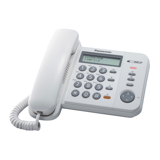
KX-TS580MXB
Model No.
KX-TS580MXW
KX-TS580MXR
KX-TS580MXC
KX-TS580MXJ
Integrated Telephone System
Black Version
White Version
Red Version
Blue Version
Ivory Version
(for Asia, Middle Near East and other areas)
© Panasonic Communications Co., Ltd. 2008. Unau-
thorized copying and distribution is a violation of law.
ORDER NO. KM40809707CE
Advertisement
Table of Contents
Troubleshooting

Related Manuals for Panasonic KX-TS580MXB


Summary of Contents for Panasonic KX-TS580MXB
- Page 1 KX-TS580MXR KX-TS580MXC KX-TS580MXJ Integrated Telephone System Black Version White Version Red Version Blue Version Ivory Version (for Asia, Middle Near East and other areas) © Panasonic Communications Co., Ltd. 2008. Unau- thorized copying and distribution is a violation of law.
- Page 2 KX-TS580MXB/KX-TS580MXW/KX-TS580MXR/KX-TS580MXC/KX-TS580MXJ...
-
Page 3: Table Of Contents
KX-TS580MXB/KX-TS580MXW/KX-TS580MXR/KX-TS580MXC/KX-TS580MXJ TABLE OF CONTENTS PAGE 1 Safety Precautions----------------------------------------------- 4 1.1. For Service Technicians --------------------------------- 4 2 Warning -------------------------------------------------------------- 4 2.1. Battery Caution--------------------------------------------- 4 2.2. About Lead Free Solder (PbF: Pb free)-------------- 4 2.3. Discarding of P.C. Board--------------------------------- 5 3 Specifications ----------------------------------------------------- 6 4 Technical Descriptions ----------------------------------------- 7 4.1. -
Page 4: Safety Precautions
KX-TS580MXB/KX-TS580MXW/KX-TS580MXR/KX-TS580MXC/KX-TS580MXJ 1 Safety Precautions 1.1. For Service Technicians • Repair service shall be provided in accordance with repair technology information such as service manual so as to pre- vent fires, injury or electric shock, which can be caused by improper repair work. -
Page 5: Discarding Of P.c. Board
KX-TS580MXB/KX-TS580MXW/KX-TS580MXR/KX-TS580MXC/KX-TS580MXJ 2.2.1. Suggested PbF Solder There are several types of PbF solder available commercially. While this product is manufactured using Tin, Silver, and Copper (Sn+Ag+Cu), you can also use Tin and Copper (Sn+Cu) or Tin, Zinc, and Bismuth (Sn+Zn+Bi). Please check the manufacturer’s specific instructions for the melting points of their products and any precautions for using their product with other materials. -
Page 6: Specifications
KX-TS580MXB/KX-TS580MXW/KX-TS580MXR/KX-TS580MXC/KX-TS580MXJ 3 Specifications Note: • Design and specification are subject to change without notice. • Specifications are subject to change without notice. Important: *: Some functions may not work properly without batteries, Refer to the Operating Instructions for details. -
Page 7: Technical Descriptions
KX-TS580MXB/KX-TS580MXW/KX-TS580MXR/KX-TS580MXC/KX-TS580MXJ 4 Technical Descriptions 4.1. Block Diagram... -
Page 8: Circuit Operation
KX-TS580MXB/KX-TS580MXW/KX-TS580MXR/KX-TS580MXC/KX-TS580MXJ 4.2. Circuit Operation 4.2.1. Bell Detector Circuit When the bell signal is input between T/R, the signal are outputted at the speaker via the following path: T / R → R1 / C1 → D1 / LED1(2AP) → IC1 (pin1) → IC1 (pin8) → PC1 → C5 → SW1 → T1 → Speaker 4.2.2. - Page 9 KX-TS580MXB/KX-TS580MXW/KX-TS580MXR/KX-TS580MXC/KX-TS580MXJ 4.2.3.3. Speakerphone Circuit 4.2.3.3.1. Function The circuit controls the automatic switching of the transmitted and received signals, to and from the telephone line, when the unit is used in the hands -free mode. 4.2.3.3.2. Circuit Operation The speakerphone can only provide a one-way communication path.
- Page 10 KX-TS580MXB/KX-TS580MXW/KX-TS580MXR/KX-TS580MXC/KX-TS580MXJ 4.2.3.4.2. Circuit operation When the batteries are inserted into the unit, then the voltage is regulated by IC302 and power is supplied to the CPU. The unit starts operating soon after the voltage goes beyond point A in the voltage diagram.
- Page 11 KX-TS580MXB/KX-TS580MXW/KX-TS580MXR/KX-TS580MXC/KX-TS580MXJ 4.2.4. Caller ID Detect Circuit 4.2.4.1. Function (FSK signal) The caller ID is a chargeable ID which the user of a telephone circuit obtains by entering a contract with the telephone company to utilize a caller ID service. For this reason, the operation of this circuit assumes that a caller ID service contract has been entered for the circuit being used.
-
Page 12: Location Of Controls And Components
KX-TS580MXB/KX-TS580MXW/KX-TS580MXR/KX-TS580MXC/KX-TS580MXJ 5 Location of Controls and 5.2. Display Components 5.1. Location of Controls Cross Reference: Battery Installation and Replacement (P.14) -
Page 13: Installation Instructions
KX-TS580MXB/KX-TS580MXW/KX-TS580MXR/KX-TS580MXC/KX-TS580MXJ 6 Installation Instructions 6.1. Connections 6.2. Connecting a Communication Device... -
Page 14: Battery
KX-TS580MXB/KX-TS580MXW/KX-TS580MXR/KX-TS580MXC/KX-TS580MXJ 6.3. Battery 6.3.1. Battery Installation and Replacement... -
Page 15: Operating Instructions
KX-TS580MXB/KX-TS580MXW/KX-TS580MXR/KX-TS580MXC/KX-TS580MXJ 7 Operating Instructions 7.1. Programmable Settings... -
Page 16: Dial Lock
KX-TS580MXB/KX-TS580MXW/KX-TS580MXR/KX-TS580MXC/KX-TS580MXJ 7.2. Dial Lock 7.3. Call Restriction... -
Page 17: Troubleshooting
KX-TS580MXB/KX-TS580MXW/KX-TS580MXR/KX-TS580MXC/KX-TS580MXJ 7.4. Troubleshooting... - Page 18 KX-TS580MXB/KX-TS580MXW/KX-TS580MXR/KX-TS580MXC/KX-TS580MXJ Cross Reference: Call Restriction (P.16) Dial Lock (P.16)
-
Page 19: Troubleshooting Guide
KX-TS580MXB/KX-TS580MXW/KX-TS580MXR/KX-TS580MXC/KX-TS580MXJ 8 Troubleshooting Guide Make sure batteries are installed for proper operation before troubleshooting. 8.1. Service Hints 8.2. Pulse Dialing Problems... -
Page 20: Tone Dialing Problems (Handset)
KX-TS580MXB/KX-TS580MXW/KX-TS580MXR/KX-TS580MXC/KX-TS580MXJ 8.3. Tone Dialing Problems (handset) 8.4. No Ringing Sound When Ring Signal is Input... -
Page 21: Disassembly And Assembly Instructions
KX-TS580MXB/KX-TS580MXW/KX-TS580MXR/KX-TS580MXC/KX-TS580MXJ 9 Disassembly and Assembly Instructions 9.1. Disassembly Instructions... - Page 22 KX-TS580MXB/KX-TS580MXW/KX-TS580MXR/KX-TS580MXC/KX-TS580MXJ...
-
Page 23: Miscellaneous
KX-TS580MXB/KX-TS580MXW/KX-TS580MXR/KX-TS580MXC/KX-TS580MXJ 10 Miscellaneous 10.1. IC Block diagram 10.1.1. IC801... - Page 24 KX-TS580MXB/KX-TS580MXW/KX-TS580MXR/KX-TS580MXC/KX-TS580MXJ 10.1.2. CPU DATA (IC801) Pin No. Description Connection Normal Standby Stop Reset SEG4 SEG4/ CMOS CMOS CMOS KeyStrobe4 SEG5 SEG5/ CMOS CMOS CMOS KeyStrobe5 SEG6 SEG6/Option CMOS CMOS CMOS Strobe SEG7 SEG7 CMOS CMOS CMOS CMOS SEG8 SEG8 CMOS...
- Page 25 KX-TS580MXB/KX-TS580MXW/KX-TS580MXR/KX-TS580MXC/KX-TS580MXJ Pin No. Description Connection Normal Standby Stop Reset IOC7_BATTDET BATT_Low IOC6_E12V BACK_UP CMOS IOC5_RDIN Ring_DET IOC4_RDRC SP_CS CMOS IOC3_SEG44 Pmute /L_SEIZ CMOS IOC2_SEG45 RELAY IOC1_SEG46 BATT_OUT IOC0_SEG47 Wake_UP IOB7 PULSE NMOS IOB6 IOB5_SEG48 EEPROM_CS CMOS IOB4_SEG49 D.I/O EEPROM_DATA IOB3_SEG50...
- Page 26 KX-TS580MXB/KX-TS580MXW/KX-TS580MXR/KX-TS580MXC/KX-TS580MXJ Pin No. Description Connection Normal Standby Stop Reset SEG1/STB1 SEG1/ CMOS CMOS CMOS CMOS KeyStrobe1 SEG2/STB2 SEG2/ CMOS CMOS CMOS CMOS KeyStrobe2 SEG3/STB3 SEG3/ CMOS CMOS CMOS CMOS KeyStrobe3...
- Page 27 KX-TS580MXB/KX-TS580MXW/KX-TS580MXR/KX-TS580MXC/KX-TS580MXJ 10.1.3. RINGER IC (IC1)
- Page 28 KX-TS580MXB/KX-TS580MXW/KX-TS580MXR/KX-TS580MXC/KX-TS580MXJ 10.1.4. EEPROM (IC851) 1. SCK SCK terminal is input terminal of Serial Clock to control transmit and receipt between Master and Slave. 2. SDA SDA terminal is input terminal, to forward the address and the mutual data between Master Device and Slave Device the mutual.
- Page 29 KX-TS580MXB/KX-TS580MXW/KX-TS580MXR/KX-TS580MXC/KX-TS580MXJ 10.1.5. Speakerphone IC Data (IC601) Name Description A resistor to ground provides a reference current for the transmit and receive attenuators. A resistor to ground determines the nominal gain of the transmit attenuator. The transmit channel gain is inversely proportional to the RTX resistance.
-
Page 30: How To Replace The Flat Package
KX-TS580MXB/KX-TS580MXW/KX-TS580MXR/KX-TS580MXC/KX-TS580MXJ 10.2. How to Replace the Flat Package IC Even if you do not have the special tools (for example, a spot heater) to remove the Flat IC, with some solder (large amount), a soldering iron and a cutter knife, you can easily remove the ICs that have more than 100 pins. - Page 31 KX-TS580MXB/KX-TS580MXW/KX-TS580MXR/KX-TS580MXC/KX-TS580MXJ 10.2.3. How to Install the IC 1. Temporarily fix the FLAT PACKAGE IC, soldering the two marked pins. *Check the accuracy of the IC setting with the corresponding soldering foil. 2. Apply flux to all pins of the FLAT PACKAGE IC.
-
Page 32: Terminal Guide Of The Ics, Transistors And Diodes
KX-TS580MXB/KX-TS580MXW/KX-TS580MXR/KX-TS580MXC/KX-TS580MXJ 10.3. Terminal Guide of the ICs, Transistors and Diodes... -
Page 33: Schematic Diagram
KX-TS580MXB/KX-TS580MXW/KX-TS580MXR/KX-TS580MXC/KX-TS580MXJ 11 Schematic Diagram 11.1. For Schematic Diagram 1. SW101: Hook switch. 2. SW1: Ringer selector. 3. DC voltage measurements are taken with electronic voltmeter from negative voltage line. 4. (Add 40 mA to telephone line from the loop simulator.) 5. -
Page 34: Schematic Diagram (Main)
KX-TS580MXB/KX-TS580MXW/KX-TS580MXR/KX-TS580MXC/KX-TS580MXJ 11.2. Schematic Diagram (Main) NC for 560RU only apply for 560RU JP11 C603 only apply for 560 (NOT RU mode) IC601 K0.027 C1CB00001673 R611 R606 R607 R612 C609 K0.1 C615 1.8K 2D2A R605 2.2M 6.3V22 R602 C606 C610 50V1 2.7K... - Page 35 KX-TS580MXB/KX-TS580MXW/KX-TS580MXR/KX-TS580MXC/KX-TS580MXJ 50V1 CONT 120K 250V1 330K 6.8K(1/2W) MESSAGE WAITING LED PULSE SHAPE only apply for PBX usage D651 Q109 (msg NC) R123 IC651 (msg NC) R124 C655 PC101 R653 JJ101 TP101 C652 (10) Ring (9.0V) R651 JJ102 EX-HOOK DETECT PULSE MUTE / LINE SEIZER...
-
Page 36: Schematic Diagram (Operation)
KX-TS580MXB/KX-TS580MXW/KX-TS580MXR/KX-TS580MXC/KX-TS580MXJ 11.3. Schematic Diagram (Operation) R558 C558 K0.1 (only apply for CID waiting) R209 COM0 TP854 C809 K0.1 COM1 IC303 C306 R305 C807 16V10 COM2 VOUT 2.7V 32K EEPROM K0.033 C806 K0.1 COM3 Q921 C808 16V10 COM4 COM5 R851 R921... - Page 37 KX-TS580MXB/KX-TS580MXW/KX-TS580MXR/KX-TS580MXC/KX-TS580MXJ Q301 1 SPTX 2 SPCS 3 MUSIC 4 BATTP D403 JP801 5 TXMUTE 6 RXMUTE C114 7 DTMF 100K D404 8 CIDW C805 K0.1 9 ACK Batt Low Detection 3.8V C804 6.3V100 10 VOL3 (10) 11 VOL2 (11) (12)
- Page 38 KX-TS580MXB/KX-TS580MXW/KX-TS580MXR/KX-TS580MXC/KX-TS580MXJ Memo...
-
Page 39: Printed Circuit Board
KX-TS580MXB/KX-TS580MXW/KX-TS580MXR/KX-TS580MXC/KX-TS580MXJ 12 Printed Circuit Board 12.1. Circuit Board (Main) 12.1.1. Component View C202 L102 SA101 PNLB1005Z KX-TS560 POS101 KX-TS580 MIC- L101 MIC+ CN902 PC101 C110 Q107 C111 Q112 C652 D103 C651 Q102 C114 Q103 R651 C106 C624 D302 D301 D602... - Page 40 KX-TS580MXB/KX-TS580MXW/KX-TS580MXR/KX-TS580MXC/KX-TS580MXJ 12.1.2. Bottom View PNLB1005Z JP11 JP51 R207 R206 R203 R202 JP13 JP12 IC201 R204 D202 C203 C205 C204 C201 R208 R205 Q201 R210 R201 C206 D201 TP604 R623 R488 TP601 Q481 R951 R484 C484 D101 Q109 R481 JA12 R483...
-
Page 41: Circuit Board (Operation)
KX-TS580MXB/KX-TS580MXW/KX-TS580MXR/KX-TS580MXC/KX-TS580MXJ 12.2. Circuit Board (Operation) 12.2.1. Component View LED1 DIAL LOCK/HOLD FUNCTION C808 CLEAR/ FLASH MUTE REDIAL/ ENTER PAUSE SP-PHONE/REDIAL LEFT RIGHT KX-TS580 CIRCUIT BOARD (Operation (Component View)) - Page 42 KX-TS580MXB/KX-TS580MXW/KX-TS580MXR/KX-TS580MXC/KX-TS580MXJ 12.2.2. Bottom View PNLB1006Z STB4 STB5 STB3 STB2 STB0 STB1 KX-TS560 KX-TS580 IC801 R306 IC303 X801 C806 R559 OPT_STB Q551 RING TP551 TP925 R560 IC301 KEYIN1 C305 R304 R303 R851 TP913 TP916 R301 R921 KEYIN4 TP915 BATTP R852 TP854...
-
Page 43: Exploded View And Replacement Parts List
KX-TS580MXB/KX-TS580MXW/KX-TS580MXR/KX-TS580MXC/KX-TS580MXJ 13 Exploded View and Replacement Parts List 13.1. Cabinet and Electrical Parts... -
Page 44: Accessories And Packing Materials
KX-TS580MXB/KX-TS580MXW/KX-TS580MXR/KX-TS580MXC/KX-TS580MXJ 13.2. Accessories and Packing Materials... -
Page 45: Replacement Part List
KX-TS580MXB/KX-TS580MXW/KX-TS580MXR/KX-TS580MXC/KX-TS580MXJ 13.3. Replacement Part List Safety Ref. Part No. Part Name & Description Remarks 1. RTL (Retention Time Limited) PNBH1003Z2 BUTTON, HOOK (for ABS-HB TS580MXB) Note: PNBH1003Z1 BUTTON, HOOK (for ABS-HB The “RTL” marking indicates that its Retention Time is TS580MXW) Limited. - Page 46 KX-TS580MXB/KX-TS580MXW/KX-TS580MXR/KX-TS580MXC/KX-TS580MXJ Safety Ref. Part No. Part Name & Description Remarks Safety Ref. Part No. Part Name & Description Remarks PQJE10110Z CONNECTOR, ZEBRA (PHOTO ELECTRIC TRANS- DUCER) 13.3.1.2. Main P.C.Board Parts 0N3181 PHOTO ELECTRIC TRANS- DUCER (RESISTORS) D0AF682JA112 6.8k Safety Ref.
- Page 47 KX-TS580MXB/KX-TS580MXW/KX-TS580MXR/KX-TS580MXC/KX-TS580MXJ Safety Ref. Part No. Part Name & Description Remarks Safety Ref. Part No. Part Name & Description Remarks R490 ERJ3GEYJ474 470k C412 ECUV1C104KBV 0.1 R491 ERJ3GEYJ334 330k C413 ECUV1C104KBV 0.1 R600 ERJ3GEYJ392 3.9k C414 ECUV1C104KBV 0.1 R601 ERJ3GEYJ103 C415 ECUV1H103KBV 0.01...
- Page 48 KX-TS580MXB/KX-TS580MXW/KX-TS580MXR/KX-TS580MXC/KX-TS580MXJ Safety Ref. Part No. Part Name & Description Remarks Safety Ref. Part No. Part Name & Description Remarks D505 MA111 DIODE(SI) C554 ECUV1H102KBV 0.001 D551 MA111 DIODE(SI) C555 ECUV1H102KBV 0.001 D552 MA111 DIODE(SI) C556 ECUV1C224KBV 0.22 D553 MA111 DIODE(SI)