Philips DVDR3305/02 Service Manual
Dvd-video recorder
Hide thumbs
Also See for DVDR3305/02:
- Quick start manual (2 pages) ,
- User manual (60 pages) ,
- Service manual (11 pages)
Table of Contents
Advertisement
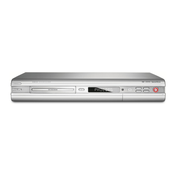
DVD-Video Recorder
Back End Repair
CLASS 1
LASER PRODUCT
Contents
1
2
3
4
5
6
7
© Copyright 2005 Philips Consumer Electronics B.V. Eindhoven, The Netherlands.
All rights reserved. No part of this publication may be reproduced, stored in a
retrieval system or transmitted, in any form or by any means, electronic,
mechanical, photocopying, or otherwise without the prior permission of Philips.
Published by KC-TE 0530 AV Systems
Version 1.1
DVDR3355/02/05/19/51 & DVDR3365/02/05/19/51
Page
2
5
7
9
12
19
19
20
21
22
23
24
25
26
26
27
28
29
30
31
32
33
34
35
Printed in the Netherlands
DVDR3305/02/05/19/51
Contents
8
9
Subject to modifi cation
Page
36
37
38
38
39
40
41
42
43
44
45
47
47
47
52
55
55
60
71
71
72
73
EN 3139 785 30931
Advertisement
Table of Contents

Related Manuals for Philips DVDR3305/02


Summary of Contents for Philips DVDR3305/02
-
Page 1: Table Of Contents
Layout: Analog-Main Part (Bottom View) Front: Front Panel © Copyright 2005 Philips Consumer Electronics B.V. Eindhoven, The Netherlands. All rights reserved. No part of this publication may be reproduced, stored in a retrieval system or transmitted, in any form or by any means, electronic, mechanical, photocopying, or otherwise without the prior permission of Philips. -
Page 2: Technical Specifi Cations And Connection Facilities
General: 1.3.4 Video Performance: Channel 25 / 503,25 MHz, Mains voltage : 220V – 240V Test pattern: PAL BG PHILIPS standard test pattern, Mains frequency : 50 Hz RF Level 74dBV Power consumption (typical) : 25 W Measured on SCART 1 Standby Power Consumption : <... -
Page 3: Video Performance
Technical Specifi cations and Connection Facilities 3139 785 3093x EN 3 1.3.6 Tuning 1.4.3 Audio/Video Front Input Connectors Audio - Cinch Automatic Search Tuning Input voltage : 2.2Vrms Scanning time without antenna : typ. 3 min. Input impedance : > 10kΩ Stop level (vision carrier) : ≥... -
Page 4: Digital Output
EN 4 3139 785 3093x Technical Specifi cations and Connection Facilities 1.6.2 Scart Audio Output voltage 2 channel mode : 1.6Vrms ± 2dB Channel unbalance (1kHz) : < 1dB Crosstalk 1kHz : > 85dB Crosstalk 16Hz-20kHz : > 70dB Frequency response 20Hz-20kHz : ± 0.2dB max Signal to noise ratio : >... -
Page 5: Safety Information, General Notes & Lead Free Requirements
Safety Information, General Notes & Lead Free Requirements 3139 785 3093x EN 5 Safety Information, General Notes & Lead Free Requirements Safety Instructions Warnings 2.1.1 General Safety 2.2.1 General Safety regulations require that during a repair: • All ICs and many other semiconductors are susceptible to •... - Page 6 “Video Plus+” and “PlusCode” are registered trademarks of workshop during a repair: the Gemstar Development Corporation. The “Video Plus+” • Use only lead-free solder alloy Philips SAC305 with order system is manufactured under licence from the Gemstar Development Corporation. code 0622 149 00106. If lead-free solder-pate is required, please contact the manufacturer of your solder-equipment.
-
Page 7: Directions For Use
Directions For Use The following except of the Quick Use Guide serves as an introduction to the set. The Complete Direction for the Use can be downloaded in different languages from the internet site of Philips Customer care Center: www.p4c.philips.com... - Page 8 DVD recorder to the corresponding AUDIO input sockets on a disappears from the display panel TV, stereo system or receiver. Turn on the connected system and before you remove the disc. select the appropriate channel. NEED HELP? Read the accompanying User Manual or visit our website www.philips.com/support...
-
Page 9: Mechanical Instructions
Mechanical Instructions 3139 785 3093x EN 9 Mechanical Instructions Dismantling and Assembly of the Set 4.1.2 Dismantling of the Front Panel Assembly 1) Remove the 3 screws 188 and release the 2 snap hooks For item numbers please see the exploded view in Chapter 9. on the side before removing the front assembly. - Page 10 EN 10 3139 785 3093x Mechanical Instructions 4.1.3 Dismantling of the Basic Engine 4.1.4 Dismantling of the Digital Board 1) Remove the Cover Tray (See 4.1.1). 1) Remove the 4 screws 272 to loose the Digital Board as shown in Figure 4-7. 2) Remove the 4 screws 260 to free the Basic Engine.
- Page 11 Mechanical Instructions 3139 785 3093x EN 11 4.1.5 Dismantling of the Analog Board 1) Remove 5 screws 244 and 4 screws 252 and screw 230. 2) Remove 4 screws 270 and 3 screws 268. 3) Service Position can be achieved by fl ipping the analog board to the Vertical Position as shown in Figure 4-9.
-
Page 12: Upgrade Software & Repair Chart
Remove disc from tray & reset system 7. Remove the Upgrade Disc and press <OK> button on Remote control to confi rm 8. The TV screen goes blank and the Philips Logo screen appear again after the tray door has closed. - Page 13 Upgrade Software & Repair Chart 3139 785 3093x EN 13 Repair Chart 5.2.1 Completely Dead Set...
- Page 14 EN 14 3139 785 3093x Upgrade Software & Repair Chart 5.2.2 Cannot Read Disk 5.2.3 Disk Unknown...
- Page 15 Upgrade Software & Repair Chart 3139 785 3093x EN 15 5.2.4 Audio No Sound (Playback)
- Page 16 EN 16 3139 785 3093x Upgrade Software & Repair Chart 5.2.5 Audio No Sound (TV & External Source)
- Page 17 Upgrade Software & Repair Chart 3139 785 3093x EN 17 5.2.6 No Video Out Upon Power ON (Assume set is not dead)
- Page 18 EN 18 3139 785 3093x Upgrade Software & Repair Chart 5.2.7 No Video In Only 5.2.8 Tuner Not Functioning...
-
Page 19: Block Diagrams,Waveforms, Wiring Diagram
Block Diagrams, Waveforms, Wiring Diagram. 3139 785 3093x EN 19 Block Diagrams, Waveforms, Wiring Diagram Overall Block Diagram of the Set Front Keyboards ANALOG BOARD 1201 CONTROL LINES, AND SUPPLY LINES CONTROL LINES 1922 AFCRI AFCLI CVBSFIN AUDIO L CONTROL UNIT SLAVE CFIN MICROPROCESSOR YFIN... -
Page 20: Control Block Diagram
Block Diagrams, Waveforms, Wiring Diagram. 3139 785 3093x EN 20 Control Block Diagram Control Block Diagram Analog Board Front FAN_CTRL Keys I2C Bus ASP Analog Slave Processor Repeater NEC uPD-16316GBT Reset HOST_Reset >=1 Reset 5VSTBY Supply Display FRONT Board IDE0 DVDR >=1 Multi Sound... -
Page 21: Wiring Diagram
Block Diagrams, Waveforms, Wiring Diagram. 3139 785 3093x EN 21 Wiring Diagram Interconnection Diagram Architecture FRONT PCB MAINS KB_FC KB_FC 1600 1800 1205 1206 1802 1803 1201 CORD MAINS P A_YG FAN_P MAINS L SCL0 GNDV FAN_N DAOUT 8008 SDA0 A_UB D_FM D_FM... -
Page 22: Waveforms Of Analog Board
Block Diagrams, Waveforms, Wiring Diagram. 3139 785 3093x EN 22 Waveforms Waveforms of Analog Board F204 BOUT F206 GOUT F207 ROUT F209 YCVBS_OUT1 F417 VDrain (No Disc) F417 Vdrain(Standby) F602 CVBS F604 Y_OUT F605 C_OUT I110 SIFOUT I303 AFER I304 AFEL I310 ARADC I311 ALADC I315 AOUT1L... -
Page 23: Waveforms Of Digital Board
Block Diagrams, Waveforms, Wiring Diagram. 3139 785 3093x EN 23 Waveforms of Digital Board IC 7211 PIN 45 IC 7211 PIN 46 IC 7401 PIN74 IC 7401 PIN75 T121 T525, T526,T529 T527,T531,T535 SY_RE,SY_FR, CY T122 T351 IC7301 PIN 42 T352 IC 7301 PIN 43 CVBS_TU, CVBS_RE,CVBS_FR T528,T530 SC_RE, SC_FR T532 BPr... -
Page 24: Test Point Overview For Analog Board
Block Diagrams, Waveforms, Wiring Diagram. 3139 785 3093x EN 24 Test Points Overview for Analog Board Analog Board TestPoint.pdf 2005-07-15... -
Page 25: Test Point Overview For Digital Board
Block Diagrams, Waveforms, Wiring Diagram. 3139 785 3093x EN 25 Test Points Overview for Digital Board Digital Board TestPoint.pdf 2005-07-15... -
Page 26: Circuit Diagram And Pwb Layout
Circuit Diagrams and PWB Layouts 3139 785 3093x EN 26 Circuit Diagrams and PWB Layouts Analog: Frontend Video (FV) 0803 H2 1100 G1 2100 C2 2101 C3 2102 B6 2103 D4 2104 E5 2105 E6 2106 F5 2107 G3 2108 G3 from PS 2109 H5 2110 H5... -
Page 27: Analog: Video In / Out (Iov)
Circuit Diagrams and PWB Layouts 3139 785 3093x EN 27 Analog: Video In / Out (IOV) 1201-1 A8 6215 B7 1201-2 A14 6217 B8 1201-3 A9 6218 B6 1204 I12 6219 C10 1205 I1 6220 C12 from PS from CINCH 1201-3 1206 I10 6221 C11... -
Page 28: Analog: Audio In / Out (Ioa)
Circuit Diagrams and PWB Layouts 3139 785 3093x EN 28 Analog: Audio In / Out (IOA) 2300 B1 I315 D9 2301 B1 I316 E6 2302 C2 I317 E9 2303 C2 I318 C2 from PS I320 B2 2304 C2 2305 C2 5VSTBY 5VSTBY 5NSTBY... -
Page 29: Analog: Power Supply (Ps)
Circuit Diagrams and PWB Layouts 3139 785 3093x EN 29 Analog: Power Supply (PS) U60 E5 3447 B13 F413 E4 U61 F3 3448 B13 F414 F4 U62 F5 3449 B13 F415 G1 U63 G4 3450 B13 F416 G1 U64 G5 3451 D10 F417 F6 1406... -
Page 30: Analog: Multi Sound Processing (Msp)
Circuit Diagrams and PWB Layouts 3139 785 3093x EN 30 Analog: Multi Sound Processing (MSP) 1500 F6 I522 D7 2500 A2 I523 E7 2501 C2 I524 D8 2502 C2 I525 E8 5VSTBY 2503 D1 I526 D8 from PS 8VSTBY 2504 D1 I527 F8 8VSTBY 3511... -
Page 31: Analog: Audio Converter (Dac_Adc)
Circuit Diagrams and PWB Layouts 3139 785 3093x EN 31 Analog: Audio Converter (DAC_ADC) 1700 E1 7706 C8 2700 B1 9014 F5 2701 B3 F700 C1 from PS 2702 D3 F701 C1 2703 D3 F702 C1 12VSTBY 3V3SW 5VSTBY 5NSTBY 2704 D3 F703 D1 2705 D3... -
Page 32: Analog: Digital In / Out 1 (Digio 1)
Circuit Diagrams and PWB Layouts 3139 785 3093x EN 32 Analog: Digital In / Out 1 (DIGIO 1) 0007 F2 1900 C9 1901 D9 2900 A4 2901 A4 2902 D2 2903 E4 2904 D5 2905 D7 2906 D8 2907 F8 3900 C2 I900 3901 B3... -
Page 33: Layout: Analog-Main Part (Top View)
Circuit Diagrams and PWB Layouts 3139 785 3093x EN 33 Layout: Analog-Main Part (Top View) Analog_Topview_3355_02.pdf 2005-07-15... -
Page 34: Layout: Analog-Main Part (Bottom View)
Circuit Diagrams and PWB Layouts 3139 785 3093x EN 34 Layout: Analog-Main Part (Bottom View) Analog_Bottomview_3355_02.pdf 2005-07-15... -
Page 35: Front: Front Panel
Circuit Diagrams and PWB Layouts 3139 785 3093x EN 35 Front: Front Panel 0100 E3 4101 I4 I107 A4 1100 E10 4102 F1 I108 A4 1101 F10 4103 E1 12VSTBY 1203 1102 H1 4104 D2 HUV-08SS65T I103 3104 1201 F13 4109 H11 1203 A6 4110 H11... -
Page 36: Front: Front Panel
Circuit Diagrams and PWB Layouts 3139 785 3093x EN 36 Front: Front Panel 1202 B1 1300 C3 1301 D1 1401 E1 3200 1402 E3 5VSTBY 5ESD 2200 A1 2201 A2 2202 A2 2203 A3 2204 B1 2205 D2 2206 D2 2207 B2 5ESD 5ESD... -
Page 37: Layout: Front Panel (Top View)
Circuit Diagrams and PWB Layouts 3139 785 3093x EN 37 Layout: Front Panel (Top View) FrontPanel_Topview_31947_3355.pdf 2005-07-15... -
Page 38: Front: Standby
Circuit Diagrams and PWB Layouts 3139 785 3093x EN 38 Front: Standby Layout: Standby (Top View) 1302 C2 1303 C4 2300 D2 6300 D2 6301 D3 F300 C2 F301 C2 I300 C4 1302 1303 I300 F300 EVQ11L05R S2B-EH F301 3139 243 32017 2005-04-12 FrontPanel_Topview_hmc1_32017_3355_02.pdf 2005-07-15... -
Page 39: Digital: Back-End Processor
Circuit Diagrams and PWB Layouts 3139 785 3093x EN 39 Digital: Back-End Processor 1101 B10 3176-4 H1 1111 E10 3177-1 I1 2101 B10 3177-2 I1 2102 B11 3177-3 I1 2105 G12 3177-4 I1 2108 F1 3178-1 I1 Back-end Flash (BEF) Communication (COM) 2109 F2 3178-2 I1... -
Page 40: Digital: Memory
Circuit Diagrams and PWB Layouts 3139 785 3093x EN 40 Digital: Memory 2201 D1 3277-2 F12 2202 D2 3277-3 F12 2203 D3 3277-4 F12 2204 D4 3281-1 F12 2205 D3 3281-2 F12 2211 B5 3281-3 F12 Memory 2212 B5 3281-4 F12 2213 B5 3283 G12 2214 B5... -
Page 41: Digital: Ieee 1394 Physical Layer
Circuit Diagrams and PWB Layouts 3139 785 3093x EN 41 Digital: IEEE 1394 Physical Layer 1351 D5 2301 D6 2302 D6 2303 D6 2304 D6 2305 D7 2306 D7 IEEE1394 Physical Layer 2307 D7 2321 G5 2341 G9 2343 G9 2351 D5 2352 E5 2361 E5... -
Page 42: Digital: Video Input Processor
Circuit Diagrams and PWB Layouts 3139 785 3093x EN 42 Digital: Video Input Processor 1461 C6 2401 C2 2402 C2 2403 C2 2404 C2 2411 D2 Video Input Processor 2412 D2 2413 D2 2414 D2 2415 D2 2421 E2 2422 E2 2423 E2 2424 E2 2425 E2... -
Page 43: Digital: Interfaces
Circuit Diagrams and PWB Layouts 3139 785 3093x EN 43 Digital: Interfaces 1501 C1 3575-3 G2 T587 G1 1502 H9 3575-4 G2 T588 G1 1512 H12 3576-1 G2 T589 G1 1521 A9 3576-2 G2 T590 H1 1522 A9 3576-3 G2 T591 H1 1536 A13 3576-4 G2... -
Page 44: Layout: Digital-Main Part (Top View)
Circuit Diagrams and PWB Layouts 3139 785 3093x EN 44 Layout: Digital-Main Part (Top View) Digital_Topview_3355_02.pdf 2005-07-15... -
Page 45: Layout: Digital-Main Part (Bottom View)
Circuit Diagrams and PWB Layouts 3139 785 3093x EN 45 Layout: Digital-Main Part (Bottom View) Digital_Bottomview_3355_02.pdf 2005-07-15... - Page 46 Circuit Diagrams and PWB Layouts 3139 785 3093x EN 46 Notes:...
-
Page 47: Circuit- And Ic Description
Circuit- and IC description 3139 785 3093x EN 47 Circuit- and IC description 8.1. Front Board (Panel – Display + Key) 8.2. Analog Board 8.1.1. General 8.2.1. General The pc board consist of the following parts: • This board consists of the following parts: Fan Control (OPTION) •... - Page 48 EN 48 3139 785 3093x Circuit- and IC Description 8.2.4. Tuner Frontend [1100 : TMQZ2] It has a RF IN for antenna connection and RF OUT which provides a RF loop through for connection to the TV. The Frontend ( Tuner & IF-demodulator ) is controlled by I (SCL_5V- and SDA_5V-) lines coming from the Domino Host on the Digital board.
- Page 49 Circuit- and IC description 3139 785 3093x EN 49 8.2.5. Audio routing Figure 8-1 Analog Audio In / Out Overview...
- Page 50 EN 50 3139 785 3093x Circuit- and IC Description The sound processing is always done in stereo (that means separate left- and right- channel) and the complete switching is realized by using HEF4052 which is a dual four-to-one multiplexer and MSP3415G which is a multi-sound processor. a) Scart 1 –...
- Page 51 Circuit- and IC description 3139 785 3093x EN 51 8.2.7. Video-routing Figure 8-2 Analog Video In / Out Overview...
-
Page 52: Digital Board
EN 52 3139 785 3093x Circuit- and IC Description 8.3. Digital Board A matrix switch STV6618 [7210] controlled by the Domino Host via I C-bus is used for Video I/O switching. All used outputs excluding pin 21 (Y/CVBS-REC) have a 6dB- The Digital Board is based on the highly integrated LSI amplifi... - Page 53 Circuit- and IC description 3139 785 3093x EN 53 Video Part ATAPI connector 1571. The analogue video input signals CVBS, YC and RGB are It buffers the data streams that are coming from (or going to) routed via the board to connector 1521 and sent to Video the Basic Engine.
- Page 54 EN 54 3139 785 3093x Circuit- and IC Description 8.3.5. Power Supply • 2.5V supply for the SDRAM is generated by an ultra fast The Digital board is not powered in standby mode. The low dropout linear regulator [7515] control signal STBY on the analog board will enable the PSU •...
-
Page 55: Ic Description
Circuit- and IC description 3139 785 3093x EN 55 IC Description 8.4.1 Analog Board IC7421 - TEA1507 - SMPS Control IC BLOCK DIAGRAM SUPPLY START-UP V CC DRAIN MANAGEMENT CURRENT SOURCE clamp internal UVLO start n.c. VALLEY supply M-level VOLTAGE CONTROLLED LOGIC OSCILLATOR... - Page 56 EN 56 3139 785 3093x Circuit- and IC Description IC7500 - MSP34X5G - Multistand Sound Processor Family BLOCK DIAGRAM 23 24 28 32 ANA_IN+ DACM_L Loud- Pre- speaker processing Modulator sound ANA_IN- DACM_R proeessing I2S_DA_IN1 Loud- Pre- speaker I2S_DA_OUT processing sound I2S_DA_IN2 proeessing...
- Page 57 Circuit- and IC description 3139 785 3093x EN 57 PIN CONFIGURATION VREF1 DACM_L SC1_OUT_R DACM_R SC1_OUT_L VREF2 AHVSUP 33 32 31 30 29 28 27 26 25 24 23 CAPL_M RESETQ AHVSS I2S_DA_IN2 AGNDC DVSS SC2_IN_L DVSUP SC2_IN_R ADR_CL MSP 34x5G I2S_DA_IN1 SC1_IN_L I2S_DA_OUT...
- Page 58 EN 58 3139 785 3093x Circuit- and IC Description PIN DESCRIPTION AND CONFIGURATION SDIN SCLK AMUTEC LRCK AOUTA MCLK VA_H AOUTB DIF1(SCL/CCLK) BMUTEC DIF0(SDA/CDIN) DEM(AD0/CS) VBIAS Pin Name Pin Description SDIN Serial Audio Data Input ( Input ) - Input for two’s complement serial audio data. SCLK Serial Clock ( Input ) - Serial clock for the serial audio interface.
- Page 59 Circuit- and IC description 3139 785 3093x EN 59 IC7704 - UDA1361TS - 96KHz Sampling 24-bit stereo audio ADC BLOCK DIAGRAM V DDA V SSA V RP V RN V ref SYSCLK V DDD UDA1361TS V SSD V INL ΣΔ MSSEL DECIMATION CLOCK...
-
Page 60: Digital Board
EN 60 3139 785 3093x Circuit- and IC Description 8.4.2 Digital Board IC7301 - TSB41AB1 - IEEE 1394a-2000 one port cable Transceiver/Arbiter BLOCK DIAGRAM Received Data Decoder/Retimer Link CNA † Interface SYSCLK LREQ TPA+ CTL0 TPA– CTL1 Cable Port TPB+ Arbitration and Control TPB–... - Page 61 Circuit- and IC description 3139 785 3093x EN 61 PIN CONFIGURATION PHP package terminal diagram PHP PACKAGE (TOP VIEW) 47 46 45 44 43 40 39 38 AGND SYSCLK CTL0 CTL1 AGND TPBIAS TSB41AB1 TPA+ TPA– TPB+ TPB– AGND 14 15 17 18 19 20 21 22 23 24 Figure 8-12...
- Page 62 EN 62 3139 785 3093x Circuit- and IC Description PIN DESCRIPTION TERMINAL TYPE TYPE DESCRIPTION DESCRIPTION NAME PHP NO. AGND 26, 32, 36 Supply – Analog circuit ground terminals. These terminals should be tied together to the low-impedance circuit board ground plane. AV DD 25, 35 Supply...
- Page 63 Circuit- and IC description 3139 785 3093x EN 63 TERMINAL TYPE TYPE DESCRIPTION DESCRIPTION NAME PHP NO. DGND 14, 46, 47 Supply – Digital circuit ground terminals. These terminals should be tied together to the low-impedance circuit board ground plane. DV DD 21, 44, 45 Supply...
- Page 64 EN 64 3139 785 3093x Circuit- and IC Description TERMINAL TYPE TYPE DESCRIPTION DESCRIPTION NAME PHP NO. PLLGND Supply – PLL circuit ground terminals. These terminals should be tied together to the low-impedance circuit board ground plane. PLLV DD Supply –...
- Page 65 Circuit- and IC description 3139 785 3093x EN 65 IC7401 - TVP5146PFP - 4x10bit DigitalVideo Decoder with microvision BLOCK DIAGRAM Copy CVBS/Y/G Protection Data Detector Slicer Analog Front End VI_1_A Composite and S-Video Processor CVBS/ VI_1_B ADC1 Pb/B/C VI_1_C Luma CVBS/Y Separation Processing...
- Page 66 EN 66 3139 785 3093x Circuit- and IC Description PIN DESCRIPTION TERMINAL DESCRIPTION DESCRIPTION NAME NUMBER Analog Video VI_1_A VI_1_x: Analog video input for CVBS/Pb/B/C VI_1_B VI_2_x: Analog video input for CVBS/Y/G VI_1_C VI_3_x: Analog video input for CVBS/Pr/R/C VI_2_A VI_4_A: Analog video input for CVBS/Y VI_2_B Up to 10 composite, 4 S-video, and 2 composite or 3 component video inputs (or a combination thereof)
- Page 67 Circuit- and IC description 3139 785 3093x EN 67 TERMINAL DESCRIPTION DESCRIPTION NAME NUMBER Host Interface I 2 C clock input I 2 C data bus Power Supplies AGND Analog ground. Connect to analog ground. A18GND_REF Analog 1.8-V return A18VDD_REF Analog power for reference 1.8 V CH1_A18GND CH2_A18GND...
- Page 68 EN 68 3139 785 3093x Circuit- and IC Description IC7501 - TPS2041 - Power Distribution Switches BLOCK DIAGRAM Power Switch † Charge Pump Current Driver Limit UVLO Thermal Sense † Current Sense Figure 8-15 PIN CONFIGURATION TPS2041 D OR P PACKAGE (TOP VIEW) Figure 8-16...
- Page 69 Circuit- and IC description 3139 785 3093x EN 69 PIN DESCRIPTION TERMINAL DESCRIPTION DESCRIPTION NAME D OR P TPS2041 TPS2051 – Enable input. Logic low turns on power switch. – Enable input. Logic high turns on power switch. Ground 2, 3 2, 3 Input voltage Over current.
- Page 70 EN 70 3139 785 3093x Circuit- and IC Description IC7595 - NCP303 - Voltage Detector Series with Programmable Delay BLOCK DIAGRAM NCP303LSNxxT1 Open Drain Output Configuration Input Reset Output Figure 8-17 PIN DESCRIPTION AND CONFIGURATION PIN CONNECTIONS AND MARKING DIAGRAM Reset Output Input...
-
Page 71: Exploded View & Spare Parts List
Exploded View & Spare Parts List 3139 785 3093x EN 71 Exploded View of the Set Figure 9-1... -
Page 72: Spare Parts List
Exploded View & Spare Parts List EN 72 3139 785 3093x Spare Parts List 0002 3139 247 11131 MODULE DRIVE D4.3 0164 3103 601 20231 SPRING GROUND 0168 3103 601 20212 SPRING I-LINK 0196 3139 241 22761 COVER TOP DVDR3305 0228 3139 241 22791 PLATE REAR EU DVDR3305 0288 4822 532 60948... -
Page 73: Revision List
Revision List 3139 785 3093x EN 73 REVISION LIST Version 1.0 * Original Release Version 1.1 * Add missing Exploded View drawing...