Table of Contents
Advertisement
Quick Links
QQ
3 7 63 1515 0
SERVICE MANUAL
Ver 1.4 2003.01
HCD-PX5 is the Amplifier, CD player, MD
Deck and Tuner section in CMT-PX5.
US and foreign patents licensed from Dolby
Laboratories.
TE
L 13942296513
Amplifier section
Tourist model:
Continuous RMS power output (Reference):
20 + 20 watts (6 ohms at 1 kHz,
10% THD, 240 V)
Other models:
Continuous RMS power output (Reference):
20 + 20 watts (6 ohms at 1 kHz,
10% THD, 220 V)
Inputs
TAPE IN (phono jacks): voltage 250 mV, impedance
47 kilohms
DIGITAL OPTICAL IN (Supported sampling frequencies:
32 kHz, 44.1 kHz and 48 kHz)
ANALOG IN (stereo minijack):
voltage 250 mV, impedance
47 kilohms
Outputs
TAPE OUT (phono jacks):voltage 250 mV, impedance
1 kilohm
PHONES (stereo minijack):
accepts headphones of 8 ohms or
more.
SPEAKER:
accepts impedance of 6 to 16
ohms.
CD player section
System
Compact disc and digital audio
system
Laser
Semiconductor laser (λ=800 nm)
Emission duration: continuous
Max. 44.6 µW*
Laser output
www
* This output is the value
measured at a distance of 200 mm
from the objective lens surface on
the Optical Pick-up Block with a
7 mm aperture.
Frequency response
2 Hz – 20 kHz
.
Sony Corporation
9-929-568-15
2003A0500-1
Home Audio Company
C 2003.01
Published by Sony Engineering Corporation
http://www.xiaoyu163.com
MD deck section
System
Laser
Laser output
Sampling frequency
Frequency response
Tuner section
FM stereo, FM/AM superheterodyne tuner
FM tuner section
Tuning range
Tourist model:
Other models:
Aerial
Aerial terminals
Intermediate frequency
AM tuner section
Tuning range
Aerial
Intermediate frequency
x
ao
u163
y
i
http://www.xiaoyu163.com
HCD-PX5
2 9
8
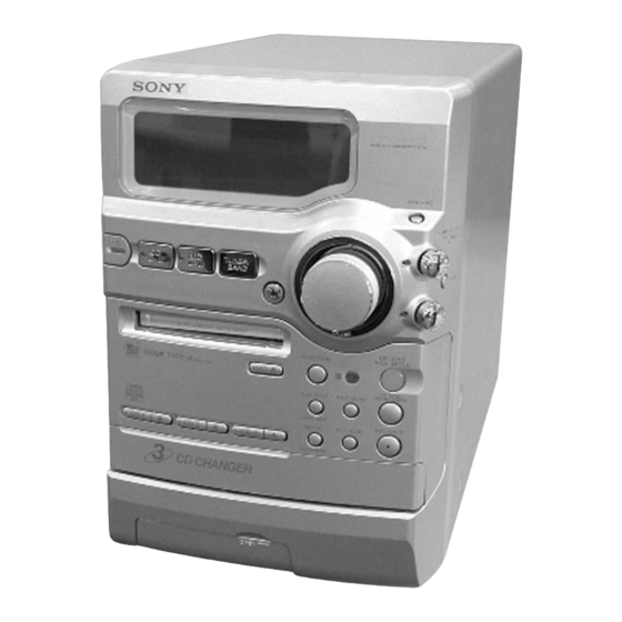
Photo: Silver model
Model Name Using Similar Mechanism
MD
MD Mechanism Type
Section
Optical Pick-up Name
Model Name Using Similar Mechanism
CD
CD Mechanism Type
Q Q
Section
Base Unit Name
3
6 7
1 3
1 5
Optical Pick-up Name
SPECIFICATIONS
MiniDisc digital audio system
Semiconductor laser (λ=780 nm)
Emission duration: continuous
Max. 44.6 µW*
* This output is the value
measured at a distance of 200 mm
from the objective lens surface on
the Optical Pick-up Block with a
7 mm aperture.
44.1 kHz
5 Hz – 20 kHz
76.0 – 108.0 MHz
(50 kHz step)
87.5 – 108.0 MHz
(50 kHz step)
FM lead aerial
75 ohms unbalanced
10.7 MHz
531 – 1,602 kHz
(with the interval set at 9 kHz)
530 – 1,710 kHz
(with the interval set at 10 kHz)
AM loop aerial
External aerial terminals
450 kHz
COMPACT DISC DECK RECEIVER
co
.
9 4
2 8
E Model
Tourist Model
HCD-MD595
MDM-7X2A
KMS-262A/J1N
NEW
CDM63-21BD53
BU-21BD53
0 5
8
2 9
9 4
2 8
OP Assy (A-MAX. 2)
General
Power requirements
Tourist model:
110 – 120 V or 220 – 240 V
AC, 50/60 Hz
Adjustable with voltage selector
Other models:
220 V AC, 50/60 Hz
Power consumption
Tourist model:
75 watts during normal operation
240 V AC
Other models:
60 watts during normal operation
Dimensions (w/h/d) incl. projecting parts and controls
Approx. 175 × 250 × 370 mm
Mass
Approx. 7.5 kg
Design and specifications are subject to change
without notice.
m
9 9
9 9
Advertisement
Table of Contents

Related Manuals for Sony HCD-PX5


Summary of Contents for Sony HCD-PX5
- Page 1 3 7 63 1515 0 SERVICE MANUAL E Model Tourist Model Ver 1.4 2003.01 HCD-PX5 is the Amplifier, CD player, MD Deck and Tuner section in CMT-PX5. Photo: Silver model US and foreign patents licensed from Dolby Model Name Using Similar Mechanism HCD-MD595 Laboratories.
-
Page 2: Self-Diagnosis Function
There is an error in the internal data that the not meet the standards. system needs in order to operate. cReplace the MD and start recording over from cConsult your nearest Sony dealer. the beginning. E0101/LASER NG C13/Read Error There is a problem with the optical pickup. - Page 3 http://www.xiaoyu163.com 3 7 63 1515 0 ITEMS OF ERROR HISTORY MODE ITEMS AND CONTENTS Display Details of History op rec tm Cumulative recording time is displayed. When cumulative recording time is over 1 minute, the hour and minute are displayed as they are. When it is under 1 minute, “Under 1 min”...
- Page 4 http://www.xiaoyu163.com 3 7 63 1515 0 Table of Error Codes Error Code Details of Error Loading failed Loading switch combination is illegal Head of PTOC could not be read within the specified time Head of PTOC could be read but its content is erroneous Access to UTOC could not be made within the specified time...
- Page 5 http://www.xiaoyu163.com 3 7 63 1515 0 4. Display of No Disc Error History CD SECTION Procedure: [ENTER/YES] 1. In the CD test mode menu, turn the knob to PROCEDURE FOR USING THE SELF-DIAGNOSIS display “dvt ECODE BU”. FUNCTION (ERROR HISTORY DISPLAY MODE) 2.
-
Page 6: Table Of Contents
AND IN THE PARTS LIST ARE CRITICAL TO SAFE 6-30. Schematic Diagram OPERATION. REPLACE THESE COMPONENTS WITH – POWER/SELECTOR Boards – ........79 SONY PARTS WHOSE PART NUMBERS APPEAR AS 6-31. IC Pin Function Description .......... 83 SHOWN IN THIS MANUAL OR IN SUPPLEMENTS PUB- LISHED BY SONY. -
Page 7: Servicing Notes
http://www.xiaoyu163.com SECTION 1 3 7 63 1515 0 SERVICING NOTES MODEL IDENTIFICATION NOTES ON HANDLING THE OPTICAL PICK-UP BLOCK OR BASE UNIT — Back panel — The laser diode in the optical pick-up block may suffer electro- static break-down because of the potential difference generated by the charged electrostatic load, etc. - Page 8 http://www.xiaoyu163.com 3 7 63 1515 0 MC COLD RESET • The cold reset clears all data including preset data stored in the RAM to initial conditions. Execute this mode when returning the set to the customer. Procedure: 1. Press the button to turn the power on.
- Page 9 http://www.xiaoyu163.com 3 7 63 1515 0 MD SECTION JIG FOR CHECKING BD (MD) BOARD WAVEFORM The special jig (J-2501-196-A) is useful for checking the waveform of the BD (MD) board. The names of terminals and the checking items to be performed are shown as follows. I+3V : For measuring IOP (Check the deterioration of the optical pick-up laser) IOP : For measuring IOP (Check the deterioration of the optical pick-up laser) GND : Ground...
- Page 10 http://www.xiaoyu163.com 3 7 63 1515 0 IOP DATA RECORDING AND DISPLAY WHEN OPTICAL PICK-UP AND NON-VOLATILE MEMORY (IC195 OF BD (MD) BOARD) ARE REPLACED The IOP value labeled on the optical pick-up can be recorded in the non-volatile memory. By recording the value, it will eliminate the need to look at the value on the label of the optical pick-up.
- Page 11 http://www.xiaoyu163.com 3 7 63 1515 0 RETRY CAUSE DISPLAY MODE IN MD • In this test mode, the causes for retry of the unit during recording can be displayed on the liquid crystal display. During playback, the “track mode” for obtaining track information will be set. This is useful for locating the faulty part of the unit.
- Page 12 http://www.xiaoyu163.com 3 7 63 1515 0 Reading the Retry Cause Display Higher Bits Lower Bits Hexa- Details Hexadecimal decimal When 0 When 1 b7 b6 b5 b4 b3 b2 b1 b0 Binary Emphasis OFF Emphasis ON Monaural Stereo This is 2-bit display. Normally 01. 01: Normal audio.
- Page 13 http://www.xiaoyu163.com 3 7 63 1515 0 CD SECTION CD AGING MODE Procedure: 1. Press the button to turn the power on. [FUNCTION] 2. Press the button to set the CD function, insert a disc to the each disc tray (CD1 to 3). [ENTER/YES] [CD3] [ENTER/YES]...
- Page 14 http://www.xiaoyu163.com 3 7 63 1515 0 CD-TEXT TEST DISC This unit is able to display the test data (character information) written in the CD on its fluorescent indicator tube. The CD-TEXT TEST DISC (TGCS-313:4-989-366-01) is used for checking the display. To check, perform the following procedure.
- Page 15 http://www.xiaoyu163.com 3 7 63 1515 0 Table 2: CD-TEXT TEST DISC Recorded Contents and Display (In this unit, some special characters cannot be displayed. This is not a fault) TRACK Recorded contents Display T All the same ! ” # $ % & ´ (21h to 27h)1kHz 0dB L&R + , –...
-
Page 16: General
http://www.xiaoyu163.com SECTION 2 3 7 63 1515 0 GENERAL LOCATION OF CONTROLS • Front View 1 I/1 button and indicator 2 Liquid crystal display 3 VOLUME knob 4 MD disc slot 5 Lid 6 CD disc tray 7 Remote sensor 8 CD N X button and indicator 9 MD N X button and indicator 0 TUNER/BAND button and indicator... - Page 17 http://www.xiaoyu163.com 3 7 63 1515 0 • Rear View 1 PC LINK jack 2 SPEAKER terminals 3 DIGITAL OPTICAL IN terminal 4 TAPE IN/OUT jacks 5 FM ANTENNA jack 6 AM ANTENNA terminals 7 AC power cord L 13942296513 Parts descriptions for the 1 ?/1 (power) switch 7 TCURSOR/CURSORt, m/M Parts descriptions for...
- Page 18 http://www.xiaoyu163.com 3 7 63 1515 0 qd PRESET EQ button Press to select the type of the preset equalizer. (page 54) qf STEREO/MONO button Press to switch between stereo and monaural when receiving a stereo broadcast. qg SCROLL button Press to display the disc title or track title scrolling.
-
Page 19: Disassembly
http://www.xiaoyu163.com SECTION 3 DISASSEMBLY 3 7 63 1515 0 • This set can be disassembled in the order shown below. CD BASE UNIT CASE (BU-21BD53) (Page 20) (Page 26) BACK PANEL, DC FAN (M801) (Page 20) MAIN BOARD, TUNER (Page 21) PANEL ASSY REG BOARD, AMP BOARD, POWER BOARD,... - Page 20 http://www.xiaoyu163.com 3 7 63 1515 0 Note: Follow the disassembly procedure in the numerical order given. CASE 2 three screws (BVTP3 × 12) 4 case 1 three screws (CASE3 TP2) 1 three screws (CASE3 TP2) L 13942296513 BACK PANEL, DC FAN (M801) 9 back panel 3 screw (BVTT3 ×...
- Page 21 http://www.xiaoyu163.com 3 7 63 1515 0 MAIN BOARD, TUNER 7 connector 7 two connectors (CN801) (CN803, 852) 7 two connectors (CN907, 908) qa harness 7 connector (CN901) q; screw (BVTT3 × 6) 8 screw (BVTT3 × 6) 5 wire (flat type) (15 core) (CN503) 9 tuner 2 connector...
- Page 22 http://www.xiaoyu163.com 3 7 63 1515 0 PANEL BOARD 5 PANEL board 4 six screws (BVTP2.6 × 8) 4 four screws (BVTP2.6 × 8) 4 three screws (BVTP2.6 × 8) 6 screw (BVTP2.6 × 8) 6 screw (BVTP2.6 × 8) 3 ring (VOL) 0 three screws (BVTP2.6 ×...
- Page 23 http://www.xiaoyu163.com 3 7 63 1515 0 BD (MD) BOARD 1 Remove the solder (four portions). 5 BD (MD) board 4 flexible board (CN101) 1 Remove the solder (five portions). L 13942296513 2 two screws (BTP2 × 6) HOLDER ASSY 1 claw 2 holder assy u163 http://www.xiaoyu163.com...
- Page 24 http://www.xiaoyu163.com 3 7 63 1515 0 GUIDE (L), SLIDER (EJ), SLIDER, LEVER (HEAD) 4 slider (EJ) 3 slider 2 guide (L) 1 two screws (BTP2 × 6) 6 lever (head) 5 lever (CHG) L 13942296513 OPTICAL PICK-UP (KMS-262A/J1N), OVER WRITE HEAD (HR901) 9 optical pick-up (KMS-262A/J1N) over write head (HR901) 8 main shaft...
- Page 25 http://www.xiaoyu163.com 3 7 63 1515 0 SPINDLE MOTOR ASSY (M101), SLED MOTOR ASSY (M102), LOADING MOTOR ASSY (M103) 1 belt (loading) 4 two screws (PWH1.7 × 2.5) 2 two screws (PWH1.7 × 2.5) 3 loading motor assy (M103) 5 sled motor assy (M102) 7 spindle motor assy (M101)
- Page 26 http://www.xiaoyu163.com 3 7 63 1515 0 POWER BOARD, POWER TRANSFORMER (T901) 4 connector (CN905) 7 four screws (BVTT3 × 6) 2 two screws (BVTP3 × 8) 4 connector (CN903) 1 connector (CN901) 6 connector (CN802) 6 connector (CN904) 5 POWER board 8 power transformer (T901) L 13942296513...
- Page 27 http://www.xiaoyu163.com 3 7 63 1515 0 CD MECHANISM DECK (CDM63-21BD53) 4 screw (BVTT3 × 6) 5 chassis assy 2 connector (CN701) 6 CD mechanism deck (CDM63-21BD53) 4 screw (BVTT3 × 6) L 13942296513 3 two screws (BVTP3 × 8) 3 two screws (BVTP3 ×...
- Page 28 http://www.xiaoyu163.com 3 7 63 1515 0 DRIVER BOARD 3 DRIVER board 1 connector (CN703) 1 connector (CN704) 1 connector (CN702) 2 screw (BTTP M2.6) 2 screw (BTTP M2.6) 1 connector (CN705) L 13942296513 FITTING BASE (STABILIZER) ASSY, TRAY ASSY, TRAY (SUB) 1 two screws (BTTP M2.6) 4 fitting base (STABILIZER) assy 1 two screws (BTTP M2.6)
- Page 29 http://www.xiaoyu163.com 3 7 63 1515 0 TRAY SENSOR BOARD 6 HOLDER (SENSOR) 2 two screws (BTTP M2.6) 5 TRAY SENSOR board 1 Rotate the cam, and lift up the stocker at the full. 4 two screws (BTTP M2.6) stocker L 13942296513 SLIDER (LOADING), GEAR (SLIDER) 3 two screws (BTTP M2.6) 4 bracket (retainer)
- Page 30 http://www.xiaoyu163.com 3 7 63 1515 0 STOCKER ASSY, TRAY (SUB) 3 stocker assy, tray (sub) 1 screw (M2.6) L 13942296513 2 Slide the slider (BU.L), slider (BU.R) in the direction of 1 screw (M2.6) arrow A at the full. DISC SENSOR BOARD 2 CD base unit assy 4 DISC SENSOR board u163...
- Page 31 http://www.xiaoyu163.com 3 7 63 1515 0 IN OUT SW BOARD 2 two screws (BTTP M2.6) 3 IN OUT SW board 1 connector (CN704) L 13942296513 MOTOR ASSY (M721), MOTOR BOARD 1 belt 2 connector (CN702) motor board bottom view u163 7 motor assy (M721) 3 Remove two solders.
-
Page 32: Test Mode
http://www.xiaoyu163.com SECTION 4 TEST MODE 3 7 63 1515 0 MD SECITON 4-1. PRECAUTIONS FOR USE OF TEST MODE • As loading related operations will be performed regardless of the test mode operations being performed, be sure to check that the disc is stopped before setting and removing it. - Page 33 http://www.xiaoyu163.com 3 7 63 1515 0 4-5. SELECTING THE TEST MODE [ENTER/YES] There are 26 types of test modes as shown below. The groups can be switched by turning the knob. After selecting the group [ENTER/YES] [ENTER/YES] to be used, press the button.
- Page 34 http://www.xiaoyu163.com 3 7 63 1515 0 4-5-1. Operating the Continuous Playback Mode 1. Entering the continuous playback mode (1) Set the disc in the unit. (Whichever recordable discs or discs for playback only are available) [ENTER/YES] (2) Turn the knob to display “CPLAY2MODE” (C36). [ENTER/YES] (3) Press the button to change the display to “CPLAY2MID”.
- Page 35 http://www.xiaoyu163.com 3 7 63 1515 0 4-7. TEST MODE DISPLAYS [CD SYNC HIGH SPEED] Each time the button is pressed, the display changes in the following order. When CPLAY or CREC are started, the display will forcibly be switched to the error rate display as the initial mode. 1.
- Page 36 http://www.xiaoyu163.com 3 7 63 1515 0 4-8. AUTOMATIC SELF-DIAGNOSIS FUNCTION This test mode performs CREC and CPLAY automatically for mainly checking the characteristics of the optical pick-up. To perform this test mode, the laser power must first be checked. Perform AUTO CHECK after the laser power check and Iop Compare. Procedure: [ENTER/YES] 1.
-
Page 37: Electrical Adjustments
http://www.xiaoyu163.com SECTION 5 ELECTRICAL ADJUSTMENTS 3 7 63 1515 0 MD SECTION 5-1. PARTS REPLACEMENT AND ADJUSTMENTS If malfunctions caused by optical pick-up such as sound skipping are suspected, follow the following check. Check before replacement Start 5-6-2. Laser Power Check (See page 40) 5-6-3. - Page 38 http://www.xiaoyu163.com 3 7 63 1515 0 Adjustment flow • Abbreviation Start OP: optical pick-up After turning off and then on the power, initialize the EEPROM Replace IC195 For details, refer to “WHEN MEMORY NG IS DIS- PLAYED” in 1. SERVICING NOTES (See page 10) 5-7.
- Page 39 http://www.xiaoyu163.com 3 7 63 1515 0 5-2. PRECAUTIONS FOR CHECKING LASER 5. When observing several signals on the oscilloscope, etc., make sure that VC and ground do not connect inside the oscil- DIODE EMISSION loscope. To check the emission of the laser diode during adjustments, never (VC and ground will become short-circuited) view directly from the top as this may lose your eye-sight.
- Page 40 http://www.xiaoyu163.com 3 7 63 1515 0 5-5. USING THE CONTINUOUSLY RECORDED Procedure: 1. Set the laser power meter on the objective lens of the optical DISC pick-up. (When it cannot be set pr operly, turn the * This disc is used in focus bias adjustment and error rate check. [CURSOR knob to move the optical pick- m ? M...
- Page 41 http://www.xiaoyu163.com 3 7 63 1515 0 5-6-4. Auto Check 5-6-6. Traverse Check This test mode performs CREC and CPLAY automatically for mainly checking the characteristics of the optical pick-up. To Note 1: Data will be erased during MO reading if a recorded disc is used in this adjustment.
- Page 42 http://www.xiaoyu163.com 3 7 63 1515 0 [ENTER/YES] 5-6-7. Focus Bias Check 9. Press the button to display “EFB = MO-P”. Then, the optical pick-up moves to the pit area automatically Change the focus bias and check the focus tolerance amount. and servo is imposed.
- Page 43 http://www.xiaoyu163.com 3 7 63 1515 0 5-7. INITIAL SETTING OF ADJUSTMENT VALUE 5-9. TEMPERATURE COMPENSATION OFFSET ADJUSTMENT Note: Save the temperature data at that time in the non-volatile memory Mode which sets the adjustment results recorded in the non-volatile as 25 ˚C reference data. memory to the initial setting value.
- Page 44 http://www.xiaoyu163.com 3 7 63 1515 0 [ENTER/YES] 6. Turn the knob so that the reading of the laser 4. After “Complete!” is displayed momentarily, the display changes [ENTER/YES] power meter becomes 6.9 to 7.1 mW, press the to “Iop 7.0 mW”. button to save it.
- Page 45 http://www.xiaoyu163.com 3 7 63 1515 0 [ENTER/YES] [ENTER/YES] 8. Turn the knob so that the waveform of the os- 18. Press the button, display “EFB = SAVE” cilloscope becomes the specified value. for a moment and save the adjustment results in the non-volatile [ENTER/YES] (When the knob is turned, the...
- Page 46 http://www.xiaoyu163.com 3 7 63 1515 0 5-14. ERROR RATE CHECK 5-16. AUTO GAIN CONTROL OUTPUT LEVEL ADJUSTMENT 5-14-1. CD Error Rate Check Be sure to perform this adjustment when the optical pick-up is Procedure: replaced. 1. Load the check disc (TDYS-1). If the adjustment results becomes “Adjust NG!”, the optical pick- [ENTER/YES] 2.
-
Page 47: Cd Section
http://www.xiaoyu163.com 3 7 63 1515 0 Adjustment and checking Loacation: CD SECTION – BD (MD) BOARD (Component Side) – Note: 1. CD Block is basically designed to operate without adjustment. There- fore, check each item in order given. D101 2. Use YEDS-18 disc (3-702-101-01) unless otherwise indicated. 3. - Page 48 http://www.xiaoyu163.com 3 7 63 1515 0 Note: A clear RF signal waveform means that the shape “◊” can be clearly Checking Location: distinguished at the center of the waveform. – BD (CD) BOARD (Conductor Side) – RF signal waveform VOLT/DIV: 200 mV TIME/DIV: 500 ns (normal speed) level: 1.2 ±...
-
Page 49: Diagrams
HCD-PX5 SECTION 6 3 7 6 3 1 5 1 5 0 DIAGRAMS 6-1. BLOCK DIAGRAM – MD SERVO Section – DIGITAL SIGNAL PROCESSOR, EFM/ACIRC ENCODER/DECODER, SHOCK PROOF MEMORY CONTROLLER, ATRAC ENCODER/DECODER OVER WRITE IC151 (1/2) EFMO ADDT DADTI... -
Page 50: Block Diagram - D/A, A/D Converter Section
HCD-PX5 3 7 6 3 1 5 1 5 0 6-2. BLOCK DIAGRAMS – D/A, A/D CONVERTER Section – VINL (Page 51) DADTI DAT AO DIGITAL DECIMATION (Page 49) CANCELLATION CONVERTER INTERFACE FILTER VINR FILTER BLOCK R-CH A/D CONVERTER... -
Page 51: Block Diagram - Main Section
HCD-PX5 3 7 6 3 1 5 1 5 0 6-3. BLOCK DIAGRAM – MAIN Section – (Page 50) J502 BUFFER IC401 TAPE OUT MUTING R-CH Q501 R-CH R-CH J702 R-CH MUTING ANALOG CONTROL Q511 J701 R-CH PHONES INPUT SELECT SWITCH,... -
Page 52: Block Diagram - Display/Power Section
HCD-PX5 3 7 6 3 1 5 1 5 0 6-4. BLOCK DIAGRAM – DISPLAY/POWER Section – LIQUID CRYSTAL DISPLAY UNIT LCD600 DATA LCD DATA LCD CLK LCD CE D771 – 776, 781 – 786 LED DRIVE DIMMER LCD BACK... -
Page 53: Note For Printed Wiring Boards And Schematic Diagrams
http://www.xiaoyu163.com 3 7 6 3 1 5 1 5 0 6-5. NOTE FOR PRINTED WIRING BOARDS AND SCHEMATIC DIAGRAMS • Circuit Boards Location (In addition to this, the necessary note is printed in each block) Note on Schematic Diagram: Note on Printed Wiring Board: •... -
Page 54: Printed Wiring Board - Bd (Cd) Board
HCD-PX5 3 7 6 3 1 5 1 5 0 6-6. PRINTED WIRING BOARD – BD (CD) Board – • See page 53 for Circuit Boards Location. 1 3 9 4 2 2 9 6 5 1 3 RELAY... -
Page 55: Schematic Diagram - Bd (Cd) Board
HCD-PX5 6-7. SCHEMATIC DIAGRAM – BD (CD) Board – • 3 7 6 3 1 5 1 5 0 See page 69 for Waveforms. 1 3 9 4 2 2 9 6 5 1 3 (Page w w w u 1 6 3 •... -
Page 56: Printed Wiring Boards - Cd Changer Section
HCD-PX5 3 7 6 3 1 5 1 5 0 6-8. PRINTED WIRING BOARDS – CD CHANGER Section – • See page 53 for Circuit Boards Location. 1 3 9 4 2 2 9 6 5 1 3 (Page 65) -
Page 57: Schematic Diagram - Cd Changer Section
HCD-PX5 3 7 6 3 1 5 1 5 0 6-9. SCHEMATIC DIAGRAM – CD CHANGER Section – • See page 80 for IC Block Diagram. 1 3 9 4 2 2 9 6 5 1 3 (Page 62) -
Page 58: Schematic Diagram - Bd (Md) Board (1/2)
HCD-PX5 6-10. SCHEMATIC DIAGRAM – BD (MD) Board (1/2) – • • See page 69 for Waveforms. See page 80 for IC Block Diagrams. 3 7 6 3 1 5 1 5 0 (Page 1 3 9 4 2 2 9 6 5 1 3... -
Page 59: Schematic Diagram - Bd (Md) Board (2/2)
HCD-PX5 3 7 6 3 1 5 1 5 0 6-11. SCHEMATIC DIAGRAM – BD (MD) Board (2/2) – • • See page 69 for Waveforms. See page 80 for IC Block Diagram. (Page 58) (Page 61) 1 3 9 4 2 2 9 6 5 1 3... -
Page 60: Printed Wiring Boards - Bd (Md) Board
HCD-PX5 3 7 6 3 1 5 1 5 0 6-12. PRINTED WIRING BOARDS – BD (MD) Board – • See page 53 for Circuit Boards Location. BD (MD) BOARD FLEXIBLE BOARD BD (MD) BOARD (CONDUCTOR SIDE) (COMPONENT SIDE) -
Page 61: Schematic Diagram - Md Digital Board (1/3)
HCD-PX5 3 7 6 3 1 5 1 5 0 6-13. SCHEMATIC DIAGRAM – MD DIGITAL Board (1/3) – • • See page 69 for Waveform. See page 80 for IC Block Diagram. (Page 59) (Page 62) 1 3 9 4 2 2 9 6 5 1 3... -
Page 62: Schematic Diagram - Md Digital (2/3)/Relay Boards
HCD-PX5 3 7 6 3 1 5 1 5 0 6-14. SCHEMATIC DIAGRAM – MD DIGITAL (2/3)/RELAY Boards – • See page 69 for Waveform. (Page 57) 1 3 9 4 2 2 9 6 5 1 3 (Page 61) -
Page 63: Schematic Diagram - Md Digital Board (3/3)
HCD-PX5 3 7 6 3 1 5 1 5 0 6-15. SCHEMATIC DIAGRAM – MD DIGITAL Board (3/3) – • • See page 69 for Waveforms. See page 80 for IC Block Diagrams. (Page 62) (Page 66) (Page 59) -
Page 64: Printed Wiring Board - Md Digital Board (Component Side)
HCD-PX5 6-16. PRINTED WIRING BOARD – MD DIGITAL Board (Component Side) – • See page 53 for Circuit Boards Location. 3 7 6 3 1 5 1 5 0 • Semiconductor Location Ref. No. Location D1104 D1106 IC1001 IC1005... -
Page 65: Printed Wiring Boards - Md Digital (Conductor Side)/Relay Boards
HCD-PX5 6-17. PRINTED WIRING BOARDS – MD DIGITAL (Conductor Side)/RELAY Boards – • See page 53 for Circuit Boards Location. 3 7 6 3 1 5 1 5 0 • Semiconductor Location Ref. No. Location D1102 D1103 D1108 IC1004... -
Page 66: Schematic Diagram - Main Board (1/2)
HCD-PX5 3 7 6 3 1 5 1 5 0 6-18. SCHEMATIC DIAGRAM – MAIN Board (1/2) – • See page 80 for IC Block Diagram. (Page 77) (Page 77) (Page 63) 1 3 9 4 2 2 9 6 5 1 3... -
Page 67: Schematic Diagram - Main Board (2/2)
HCD-PX5 6-19. SCHEMATIC DIAGRAM – MAIN Board (2/2) – • • See page 69 for Waveforms. See page 80 for IC Block Diagram. 3 7 6 3 1 5 1 5 0 (Page 74) 1 3 9 4 2 2 9 6 5 1 3... -
Page 68: Printed Wiring Board - Main Board
HCD-PX5 3 7 6 3 1 5 1 5 0 6-20. PRINTED WIRING BOARD – MAIN Board – • See page 53 for Circuit Boards Location. (Page 72) (Page 70) (Page 75) R846 1 3 9 4 2 2 9 6 5 1 3... - Page 69 http://www.xiaoyu163.com 3 7 6 3 1 5 1 5 0 • Waveforms – BD (MD) Board – – MAIN Board – – BD (CD) Board – – MD DIGITAL Board – 1 IC101 wg (MDP) (CD Play Mode) 6 IC101 us (XTAO) 1 IC101 1 (I), 2 (J) (MD Play Mode) 1 IC1101 el (X1) 1 IC506 eg (XT1)
-
Page 70: Printed Wiring Board - Amp Board
HCD-PX5 6-21. PRINTED WIRING BOARD – AMP Board – • See page 53 for Circuit Boards Location. 3 7 6 3 1 5 1 5 0 • Semiconductor (Page 76) Location Ref. No. Location D801 D802 D803 D851 D852... -
Page 71: Schematic Diagram - Amp Board
HCD-PX5 3 7 6 3 1 5 1 5 0 6-22. SCHEMATIC DIAGRAM – AMP Board – (Page 77) (Page 79) (Page 67) (Page 67) (Page 67) 1 3 9 4 2 2 9 6 5 1 3 w w w •... -
Page 72: Printed Wiring Boards - Jack/Jog Boards
HCD-PX5 3 7 6 3 1 5 1 5 0 6-23. PRINTED WIRING BOARDS – JACK/JOG Boards – • See page 53 for Circuit Boards Location. (KR) (Page 68) (KR) (KR) (Page 75) 1 3 9 4 2 2 9 6 5 1 3 (Page 68) •... -
Page 73: Schematic Diagram - Jack/Jog Boards
HCD-PX5 3 7 6 3 1 5 1 5 0 6-24. SCHEMATIC DIAGRAM – JACK/JOG Boards – (Page 67) (Page 74) 1 3 9 4 2 2 9 6 5 1 3 (Page 67) w w w u 1 6 3... -
Page 74: Schematic Diagram - Panel Board
HCD-PX5 3 7 6 3 1 5 1 5 0 6-25. SCHEMATIC DIAGRAM – PANEL Board – • See page 80 for IC Block Diagram. (Page 73) (Page 67) 1 3 9 4 2 2 9 6 5 1 3 •... -
Page 75: Printed Wiring Board - Panel Board
HCD-PX5 3 7 63 1515 0 6-26. PRINTED WIRING BOARD – PANEL Board – • See page 53 for Circuit Boards Location. (Page 68) L 13942296513 (Page 72) • Semiconductor Location Ref. No. Location Ref. No. Location Ref. No. -
Page 76: Printed Wiring Board - Reg Board
HCD-PX5 3 7 63 1515 0 6-27. PRINTED WIRING BOARD – REG Board – • See page 53 for Circuit Boards Location. (Page 78) (Page 68) (Page 68) L 13942296513 • Semiconductor (Page 70) Location Ref. No. Location D800... -
Page 77: Schematic Diagram - Reg Board
HCD-PX5 3 7 6 3 1 5 1 5 0 6-28. SCHEMATIC DIAGRAM – REG Board – (Page 66) (Page 66) 1 3 9 4 2 2 9 6 5 1 3 (Page 79) (Page 71) • Voltages and waveforms are dc with respect to ground The components identified by mark 0 or dotted under no-signal (detuned) conditions. -
Page 78: Printed Wiring Boards - Power/Selector Boards
HCD-PX5 3 7 6 3 1 5 1 5 0 6-29. PRINTED WIRING BOARDS – POWER/SELECTOR Boards – • See page 53 for Circuit Boards Location. (Page 76) (Page 68) (JE) (Page 70) SELECTOR BOARD (JE) 1-681-201- 1 3 9 4 2 2 9 6 5 1 3 (JE) •... -
Page 79: Schematic Diagram - Power/Selector Boards
HCD-PX5 3 7 6 3 1 5 1 5 0 6-30. SCHEMATIC DIAGRAM – POWER/SELECTOR Boards – (Page 67) 1 3 9 4 2 2 9 6 5 1 3 (Page 77) (Page 71) w w w • Voltages and waveforms are dc with respect to ground... - Page 80 http://www.xiaoyu163.com 3 7 6 3 1 5 1 5 0 • IC Block Diagrams IC141 BH6511FS – BD (MD) Board – IC101 CXA2523AR 43 42 INTERFACE INTERFACE USROP – RF AGC CHARGE – PREDRIVE PREDRIVE USRC RFA1 PUMP. BPF3T RFA2 RFA3 PREDRIVE PREDRIVE...
- Page 81 http://www.xiaoyu163.com 3 7 63 1515 0 – DRIVER Board – IC701 BA6956AN CONTROL LOGIC – MD DIGITAL Board – IC1004 LB1641 T.S.D O.C.P MOTOR MOTOR DRIVE DRIVE FWD/REV/STOP CONTROL LOGIC L 13942296513 IC1005 UDA1360TS VDDA VSSA 14 FSEL VINL CLOCK –...
- Page 82 http://www.xiaoyu163.com 3 7 63 1515 0 IC1006 UDA1350AH 41 40 39 38 37 36 RESET BCKO VDDD (C) VDDA (PLL) VSSD 31 VSSA (PLL) VSSD (C) PREEM1 DATA L3DATA IEC 958 OUTPUT L3CLOCK DECODER INTERFACE CLOCK INTERFACE CLKOUT DATAI TIMING DATA CIRCUIT 28 NC...
-
Page 83: Ic Pin Function Description
http://www.xiaoyu163.com 3 7 63 1515 0 6-31. IC PIN FUNCTION DESCRIPTION • BD (MD) BOARD IC101 CXA2523AR (RF AMP, FOCUS/TRACKING ERROR AMP) Pin No. Pin Name Description I-V converted RF signal I input from the optical pick-up block detector I-V converted RF signal J input from the optical pick-up block detector Middle point voltage (+1.65V) generation output terminal 4 to 9 A to F... - Page 84 http://www.xiaoyu163.com 3 7 63 1515 0 • BD (MD) BOARD IC151 CXD2662R (DIGITAL SIGNAL PROCESSOR, DIGITAL SERVO PROCESSOR, EFM/ACIRC ENCODER/DECODER, SHOCK PROOF MEMORY CONTROLLER, ATRAC ENCODER/DECODER) Pin No. Pin Name Description Focus OK signal output terminal “H” is output when focus is on (“L”: NG) MNT0 (FOK) Not used (open) MNT1 (SHOCK)
- Page 85 http://www.xiaoyu163.com 3 7 63 1515 0 Pin No. Pin Name Description XCAS Column address strobe signal output to the D-RAM (IC152) “L” active Address signal output to the D-RAM (IC152) XRAS Row address strobe signal output to the D-RAM (IC152) “L” active Write enable signal output to the D-RAM (IC152) “L”...
- Page 86 http://www.xiaoyu163.com 3 7 63 1515 0 Pin No. Pin Name Description FRDR Focus servo drive PWM signal (–) output to the BH6511FS (IC141) Clock signal (176.4 kHz) output terminal (X’tal system) Not used (open) SRDR Sled servo drive PWM signal (–) output to the BH6511FS (IC141) SFDR Sled servo drive PWM signal (+) output to the BH6511FS (IC141) SPRD...
- Page 87 http://www.xiaoyu163.com 3 7 63 1515 0 • MD DIGITAL BOARD IC1001 M30805MG-205GP (MD MECHANISM CONTROLLER) Pin No. Pin Name Description 1, 2 — Not used (open) LVL1 L-ch level output terminal Not used (open) LVL0 R-ch level output terminal Not used (open) 5 to 7 —...
- Page 88 http://www.xiaoyu163.com 3 7 63 1515 0 Pin No. Pin Name Description C2-PWM-B Not used (open) XINT Interrupt status input from the CXD2662R (IC151) — Not used (open) XELT Not used (open) Laser power select signal output to the CXD2662R (IC151) and HF module switch circuit WR-PWR “L”: playback mode, “H”: recording mode I2CCLK...
- Page 89 http://www.xiaoyu163.com 3 7 63 1515 0 Pin No. Pin Name Description VCC3 — Power supply terminal (+3.3V) Address signal output to the flash memory Not used (open) VSS3 — Ground terminal 77 to 85 A17 to A9 Address signal output to the flash memory Not used (open) 86 to 89 SEL3 to SEL0 Model destination setting input terminal...
- Page 90 http://www.xiaoyu163.com 3 7 63 1515 0 • MD DIGITAL BOARD IC1101 µPDSS3033AYGF-M10-3BA (CD MECHANISM CONTROLLER) Pin No. Pin Name Description DRVDAT Serial data output to a FL driver Not used (open) DRVCLK Serial data transfer clock signal output to a FL driver Not used (open) I2CDAT Data input/output terminal for the IIC bus Not used (open)
- Page 91 http://www.xiaoyu163.com 3 7 63 1515 0 Pin No. Pin Name Description Detection input from the disc tray 2 height sensor (IC732) TRAYSENS2 “H”: disc tray 2 position is chucking position OUT-SW Detection input from the OUT switch (S742) “L”: when sub tray is chucking position Detection input from the IN switch (S741) IN-SW “L”: when sub tray slides out of the chucking position...
- Page 92 http://www.xiaoyu163.com 3 7 63 1515 0 • MAIN BOARD IC506 µPDSS3033AYGF-M11-3BA (SYSTEM CONTROLLER) Pin No. Pin Name Description GEQ DATA Serial data output to the M62428AFP (IC505) GEQ CLK Serial data transfer clock signal output to the M62428AFP (IC505) IIC DAT Data input/output terminal for the IIC bus CANT USE Not used (fixed at “L”)
- Page 93 http://www.xiaoyu163.com 3 7 63 1515 0 Pin No. Pin Name Description SPK RELAY Speaker on/off relay (RY801) control signal output “L”: speaker off Power down detection signal output to the MD mechanism controller (IC1001) and CD MD/CD POWER mechanism controller (IC1101) “L”: power down TR RELAY Standby relay (RY961) control signal output “L”: speaker off RECMUTE...
- Page 94 http://www.xiaoyu163.com 3 7 63 1515 0 Pin No. Pin Name Description AC CUT IN AC power off detection signal input from the reset signal generator (IC508) Not used (open) RDS DATA RDS serial data input from the RDS decoder Not used (open) RDS CLK RDS serial data transfer clock signal input from the RDS decoder Not used (open) SELF WRITE IN...
-
Page 95: Exploded Views
http://www.xiaoyu163.com SECTION 7 EXPLODED VIEWS 3 7 63 1515 0 NOTE: • Items marked “*” are not stocked since they • -XX and -X mean standardized parts, so they The components identified by mark 0 or dotted line with mark may have some difference from the original are seldom required for routine service. - Page 96 http://www.xiaoyu163.com Ver 1.3 3 7 63 1515 0 (2) FRONT PANEL SECTION LCD600 not supplied (JOG board) supplied with S701 L 13942296513 not supplied (JACK board) not supplied not supplied not supplied Ref. No. Part No. Description Remark Ref. No. Part No.
- Page 97 http://www.xiaoyu163.com 3 7 63 1515 0 (3) CHASSIS SECTION not supplied not supplied (POWER board) not supplied 108 107 not supplied T901 not supplied not supplied (REG board) not supplied (AMP board) MDM-7X2A not supplied not supplied L 13942296513 CDM63-21BD53 not supplied The components identified by mark 0 or dotted line with...
- Page 98 http://www.xiaoyu163.com 3 7 63 1515 0 (4) MD MECHANISM DECK SECTION-1 (MDM-7X2A) L 13942296513 Ref. No. Part No. Description Remark Ref. No. Part No. Description Remark * 301 4-996-267-01 BASE (BU-D) 4-227-012-01 SPRING (HOLDER), TENSION 4-231-319-01 SCREW (2X6) CZN, +B (P) TRI 4-227-019-02 PLATE (HOLDER), RETAINER 4-227-007-01 GEAR (SB) 4-227-013-01 SPRING (EJ), TENSION...
- Page 99 http://www.xiaoyu163.com 3 7 63 1515 0 (5) MD MECHANISM DECK SECTION-2 (MDM-7X2A) HR901 S102 M101 L 13942296513 M102 The components identified by M103 mark 0 or dotted line with mark 0 are critical for safety. Replace only with part number specified.
- Page 100 http://www.xiaoyu163.com Ver 1.4 3 7 63 1515 0 (6) CD MECHANISM DECK SECTION-1 (CDM63-21BD53) supplied not supplied supplied not supplied not supplied L 13942296513 not supplied (TRAY SENSOR board) not supplied not supplied Ref. No. Part No. Description Remark Ref. No. Part No.
- Page 101 http://www.xiaoyu163.com 3 7 63 1515 0 not supplied (7) CD MECHANISM DECK SECTION-2 (CDM63-21BD53) not supplied (DISC SENSOR board) not supplied (IN OUT SW board) not supplied supplied not supplied L 13942296513 (DRIVER board) not supplied supplied not supplied (RELAY board) M721 The components identified by mark 0 or dotted line with...
-
Page 102: Electrical Parts List
http://www.xiaoyu163.com SECTION 8 3 7 63 1515 0 ELECTRICAL PARTS LIST NOTE: • Due to standardization, replacements in the • Items marked “*” are not stocked since they The components identified by mark 0 or dotted line with mark parts list may be different from the parts speci- are seldom required for routine service. - Page 103 http://www.xiaoyu163.com BD (MD) 3 7 63 1515 0 Ref. No. Part No. Description Remark Ref. No. Part No. Description Remark R811 1-249-417-11 CARBON 1/4W A-4725-056-A BD (MD) BOARD, COMPLETE R812 1-247-807-31 CARBON 1/4W ************************ R813 1-249-417-11 CARBON 1/4W < CAPACITOR > R814 1-249-437-11 CARBON 1/4W...
- Page 104 http://www.xiaoyu163.com BD (MD) 3 7 63 1515 0 Ref. No. Part No. Description Remark Ref. No. Part No. Description Remark C181 1-126-206-11 ELECT CHIP 100uF 6.3V L161 1-500-245-11 FERRITE C182 1-163-038-11 CERAMIC CHIP 0.1uF L171 1-500-245-11 FERRITE C183 1-164-156-11 CERAMIC CHIP 0.1uF L180 1-469-855-21 FERRITE...
- Page 105 http://www.xiaoyu163.com BD (MD) DISC SENSOR DRIVER IN OUT SW JACK 3 7 63 1515 0 Ref. No. Part No. Description Remark Ref. No. Part No. Description Remark R150 1-216-833-11 METAL CHIP 1/16W CN703 1-785-331-11 PIN, CONNECTOR (LIGHT ANGLE) 5P R151 1-216-833-11 METAL CHIP 1/16W CN704...
- Page 106 http://www.xiaoyu163.com JACK MAIN 3 7 63 1515 0 Ref. No. Part No. Description Remark Ref. No. Part No. Description Remark < RESISTOR > C355 1-110-339-11 MYLAR 220PF C357 1-126-964-11 ELECT 10uF R752 1-249-441-11 CARBON 100K 1/4W R753 1-249-441-11 CARBON 100K 1/4W C358 1-126-965-11 ELECT...
- Page 107 http://www.xiaoyu163.com MAIN 3 7 63 1515 0 Ref. No. Part No. Description Remark Ref. No. Part No. Description Remark C609 1-162-306-11 CERAMIC 0.01uF IC505 8-759-494-40 IC M62428AFP600C C611 1-162-306-11 CERAMIC 0.01uF C612 1-164-159-11 CERAMIC 0.1uF IC506 8-759-683-63 IC uPDSS3033AYGF-M11-3BA C613 1-162-306-11 CERAMIC 0.01uF IC508...
- Page 108 http://www.xiaoyu163.com MAIN 3 7 63 1515 0 Ref. No. Part No. Description Remark Ref. No. Part No. Description Remark R589 1-249-409-11 CARBON 1/4W R362 1-247-885-00 CARBON 180K 1/4W R590 1-249-417-11 CARBON 1/4W R363 1-249-433-11 CARBON 1/4W R591 1-247-843-11 CARBON 3.3K 1/4W R364 1-247-903-00 CARBON...
- Page 109 http://www.xiaoyu163.com MAIN MD DIGITAL 3 7 63 1515 0 Ref. No. Part No. Description Remark Ref. No. Part No. Description Remark R672 1-249-413-11 CARBON 1/4W C1102 1-163-038-11 CERAMIC CHIP 0.1uF R673 1-249-413-11 CARBON 1/4W C1103 1-163-038-11 CERAMIC CHIP 0.1uF C1104 1-126-960-11 ELECT R674 1-249-425-11 CARBON...
- Page 110 http://www.xiaoyu163.com Ver 1.3 MD DIGITAL MOTOR PANEL 3 7 63 1515 0 Ref. No. Part No. Description Remark Ref. No. Part No. Description Remark R1013 1-216-073-00 METAL CHIP 1/10W < VIBRATOR > R1014 1-216-073-00 METAL CHIP 1/10W X1001 1-579-175-11 VIBRATOR, CERAMIC (10MHz) R1015 1-216-073-00 METAL CHIP 1/10W...
- Page 111 http://www.xiaoyu163.com PANEL POWER 3 7 63 1515 0 Ref. No. Part No. Description Remark Ref. No. Part No. Description Remark D782 8-719-080-67 LED SELU6714C-TP6 (LCD BACK LIGHT) R741 1-249-409-11 CARBON 1/4W D783 8-719-080-67 LED SELU6714C-TP6 (LCD BACK LIGHT) R742 1-249-427-11 CARBON 6.8K 1/4W D784...
- Page 112 http://www.xiaoyu163.com POWER 3 7 63 1515 0 Ref. No. Part No. Description Remark Ref. No. Part No. Description Remark < CAPACITOR > < CAPACITOR > C901 1-126-916-11 ELECT 1000uF 6.3V C800 1-126-960-11 ELECT C902 1-126-965-11 ELECT 22uF C801 1-126-960-11 ELECT C904 1-113-342-11 CERAMIC 0.1uF...
- Page 113 http://www.xiaoyu163.com RELAY SELECTOR TRAY SENSOR 3 7 63 1515 0 Ref. No. Part No. Description Remark Ref. No. Part No. Description Remark < TRANSISTOR > 1-693-472-21 TUNER (JE) 1-693-473-41 TUNER (HK, KR) Q800 8-729-209-15 TRANSISTOR 2SD2012 1-757-087-11 WIRE (FLAT TYPE) (23 CORE) Q801 8-729-209-15 TRANSISTOR 2SD2012...
- Page 114 HCD-PX5 3 7 63 1515 0 REVISION HISTORY Clicking the version allows you to jump to the revised page. Also, clicking the version at the upper right on the revised page allows you to jump to the next revised page.