Table of Contents
Advertisement
Advertisement
Chapters
Table of Contents

Related Manuals for Panasonic DMR-EZ49VEG


Summary of Contents for Panasonic DMR-EZ49VEG
- Page 1 ORDER NO.DSD1002003CE DVD Recorder DMR-EZ49VEG Model No. DMR-EZ49VEC DMR-EZ49VEB Vol. 1 Colour (K).......Black Type (S).......Silver Type (Only EZ49VEG) © Panasonic Corporation 2010. Unauthorized copying and distribution is a violation of law.
-
Page 2: Table Of Contents
TABLE OF CONTENTS PAGE PAGE 1 Safety Precaution -------------------------------------------------3 1.1. General guidelines -----------------------------------------3 2 Warning --------------------------------------------------------------4 2.1. Prevention of Electrostatic Discharge (ESD) to Electrostatic Sensitive (ES) Devices ---------------4 2.2. Precaution of Laser Diode -------------------------------5 2.3. Service caution based on legal restrictions----------6 3 Service Navigation------------------------------------------------7 3.1. -
Page 3: Safety Precaution
1 Safety Precautions 1.1. General guidelines 1. When servicing, observe the original lead dress. If a short circuit is found, replace all parts which have been overheated or damaged by the short circuit. 2. After servicing, see to it that all the protective devices such as insulation barriers, insulation papers shields are properly installed. -
Page 4: Warning
2 Warning 2.1. Prevention of Electrostatic Discharge (ESD) to Electrostatic Sensitive (ES) Devices Some semiconductor (solid state) devices can be damaged easily by static electricity. Such components commonly are called Elec- trostatic Sensitive (ES) Devices. Examples of typical ES devices are integrated circuits and some field-effect transistor-sand semi- conductor "chip"... -
Page 5: Precaution Of Laser Diode
2.2. Precaution of Laser Diode... -
Page 6: Service Caution Based On Legal Restrictions
2.3. Service caution based on legal restrictions 2.3.1. General description about Lead Free Solder (PbF) The lead free solder has been used in the mounting process of all electrical components on the printed circuit boards used for this equipment in considering the globally environmental conservation. The normal solder is the alloy of tin (Sn) and lead (Pb). -
Page 7: Service Navigation
3 Service Navigation 3.1. Service Information 3.2. Caution for DivX (except DMR-EZ49VEB) -
Page 8: Micro Fuse Conducting Check
3.3. Micro Fuse conducting check This unit uses the Micro Fuse. Check the Micro Fuse conducting using the Tester at the check points below. -
Page 9: Operation Check When A Usb Device Is Connected
3.4. Operation check when a USB device is connected You can check the operation status (normal or abnormal) of the USB connection part of this unit easily as shown below. Connect each device to the USB terminal on the front panel and check the operation status on the TV monitor. Normal operation: Automatically displayed when the USB connection is made to a digital camera, etc. -
Page 10: Specifications
4 Specifications... -
Page 12: Location Of Controls And Components
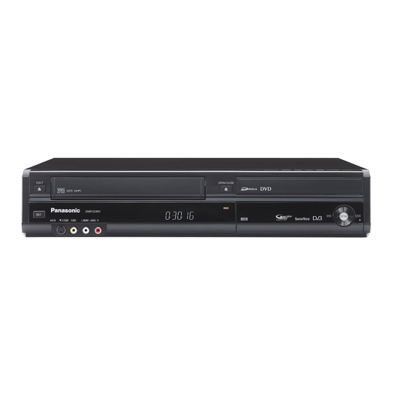
5 Location of Controls and Components 5.1. Each Buttons Followings are the Location of Controls and Components for DMR-EZ49VEB as a sample. For other models, refer to each Operating Instructions. -
Page 14: Unit When The Disc Cannot Be Ejected By Open/Close Button
6 Operating Instructions 6.1. (DVD) Taking out the Disc from DVD-Drive Unit when the Disc cannot be ejected by OPEN/CLOSE button 6.1.1. (DVD) Forcible Disc Eject 6.1.1.1. (DVD) When the power can be turned off. 1. Turn off the power and press [STOP], [CH UP] keys on the front panel simultaneously for 15 seconds. 6.1.1.2. - Page 15 1. Turn off the power and pull out AC cord. 2. Remove the Top Case. 3. Push in SLIDE CAM by Paper Clip or minus screw driver (small) to eject tray slightly. 4. Push out Tray by Paper Clip or minus screw driver (small).
-
Page 16: Vhs) Removing Cassette Tape Manually
6.2. (VHS) Removing Cassette Tape 3. Stop unloading just before unloading will be completed as manually shown below, and then the tape becomes slack as shown below. When the cassette tape could not be uninstalled from an elec- 4. Rotate the S-Reel by a small minus screwdriver to trical malfunction, there are 2 ways to remove a cassette tape. - Page 17 6.2.3. (VHS) Take out Cassette Tape man- 6. Attach Loading Motor and tighten the screw. ually after removing the mecha- 7. Set the Position Switch to EJECT POSITION certainly nism and attach the mechanism to chassis as shown below. 1. Disconnect the AC plug, and remove the Top Panel, Front Panel and the Mechanism by referring to "9 Assembling and Disassembling"...
-
Page 18: Service Mode
7 Service Mode 7.1. (DVD) Self-Diagnosis and Special Mode Setting 7.1.1. (DVD) Self-Diagnosis Functions Self-Diagnosis Function provides information for errors to service personnel by “Self-Diagnosis Display” when any error has occurred. U**, H** and F** are stored in memory and held. You can check latest error code by transmitting [0] [1] of Remote Controller in Service Mode. - Page 19 Error Code Diagnosis contents Description Monitor Display Automatic FL display ST Microprocessor Display appears when ST Microprocessor No display Communication Error Communication Error on Timer Bus occurs. Timer Bus U80 is displayed till [POWER] key is pressed. ST Microprocessor Display appears when ST Microprocessor No display Communication Error...
- Page 20 Error Code Diagnosis contents Description Monitor Display Automatic FL display NO READ Disc read error *A disc is flawed or dirty. “Cannot read. *A poor quality failed to start. Please check the *The track information could not be read. disc.” HARD Drive error The drive detected a hard error.
- Page 21 7.1.2. (DVD) Special Modes Setting Item FL display Key operation Mode name Description Front Key TEST Mode *All the main unit's parameters (include tuner) Press [VHS to DVD COPYING], are initialized. [REC] and [OPEN/CLOSE] keys simultaneously for five seconds when power is off. Rating password The audiovisual level setting password is ini- Open the tray, set DRIVE SELECT...
- Page 22 Item FL display Key operation Mode name Description Front Key Aging Contents (Example): Demonstration Ejection of the disc is prohibited. *When lock the tray. When the power is on, press lock/unlock The lock setting is effective until unlocking the [STOP] and [POWER] keys simulta- tray and not released by “Main unit initializa- neously for 5 seconds in the condi- tion”...
- Page 23 7.1.3. (DVD) Service Modes at a glance Service mode setting: While the power is off, press [STOP], [VHS to DVD COPYING] and [OPEN / CLOSE] simultaneously for five seconds. Item FL display Key operation Mode name Description (Remote controller key) Release Items Item of Service Mode executing is cancelled.
- Page 24 Item FL display Key operation Mode name Description (Remote controller key) White Picture Output White picture is output as component Output *Initial mode is “Interlace”. Press [1] [1] in service mode. from AV Decoder. *White picture (Saturation rate : 100%) *It is enable to switch Interlace/Progressive by “I/P switch: [1] [4]”...
- Page 25 Item FL display Key operation Mode name Description (Remote controller key) Laser Used Time Indi- Check laser used time (hours) of drive. Press [4] [1] in service mode. cation • (*****) is the used time display in hour. • Laser used time of DVD/ CD in Playback/Recording mode counted.
- Page 26 Item FL display Key operation Mode name Description (Remote controller key) Laser power confirma- Drive state is judged based on difference into tion between laser power value at shipping and DVD Drive in service mode. present laser power value. (Other media are assumed to be non-correspondence.) * is judgement result 2.
- Page 27 When USB check is OK. * Insert USB memory. [*] is volume label. Example of volume label is [PANASONIC] : When USB check is NG. AV4(V)/AV1(RGB) I/O Set input to AV4 (V) and set output to AV1 Press [8] [0] in service mode.
- Page 28 Item FL display Key operation Mode name Description (Remote controller key) AV2(Y/C)/AV1(V) Set input to AV2 (Y/C) and set output to AV1 Press [8] [1] in service mode. Setting (V) for I/O checking AV2(V)/AV1(Y/C) Set input to AV2 (V) and set output to AV1 (Y/ Press [8] [2] in service mode.
-
Page 29: Vhs) Self-Diagnosis And Special Mode Setting
7.2. (VHS) Self-Diagnosis and Special Mode Setting 7.2.1. (VHS) Special Modes Setting Note: Set DRIVE SELECT to VHS. Item FL display Key operation Mode name Description Front Key Tracking Center Tape Tracking is adjusted to center No display During PLAYBACK, press [CH UP] FIX position. - Page 30 7.2.2. (VHS) Service Modes 1. Set DRIVE SELECT to VHS. 2. When power is off, press [STOP] and [EJECT] keys simultaneously for 3 seconds to into Service Mode. 3. In service mode, press [STOP] and [EJECT] keys simultaneously to add Service Number. Service Contents Contents of Indication on minute...
- Page 31 7.2.3. (VHS) Self-Diagnosis Functions This model has a self-diagnosis. If the VHS section detects trouble during installation or during use, the power is automatically turned off or become power-save mode and it is memorized into the EEPROM (IC9705) as error code of two-digit number. It's mem- orized error code can be displayed in "second"...
- Page 32 7.2.3.1.4. Indication of the self-diagnosis history. The self-diagnosis histories can be indicated on the FIP with Service Mode number 3 to 5. The procedure of service mode setting and indication format are the same as usual.
-
Page 33: Service Fixture & Tools
8 Service Fixture & Tools (For DVD) Part Number Description Compatibility RFKZ0168 Extension Cable (Digital IF P.C.B. - Fan Motor / 3 Pin) Same as EZ48V Series VFK1729 Extension Cable (Main P.C.B. - Digital IF P.C.B. / 13 Pin) Same as EZ48V Series RFKZ0216 Extension Cable (Main P.C.B. -
Page 34: Disassembly Flow Chart
9 Disassembly and Assembly Instructions 9.1. Disassembly Flow Chart The following chart is the procedure for disassembling the casing and inside parts for internal inspection when carrying out the ser- vicing. To assemble the unit, reverse the steps shown in the chart below. -
Page 35: P.c.b. Positions
9.2. P.C.B. Positions... -
Page 36: Caution With Inserting Cassette Tape When Disassembling The Unit
9.3. Caution with inserting cassette tape when disassembling the unit Note1: For description of the disassembling procedure, see the section 9.4. Note2: Video Cassette might not enter when a strong lighting is applied to VHS Mechanism when Video Cassette is inserted. Please weaken the lighting or cover with the top panel etc. -
Page 37: Top Case
9.4. Top Case 3. Make the unit turn inside out, push the tabs (E) - (H) by (-) screwdriver while pulling Front Panel in the direction of 1. Remove 4 Screws (A) and 3 Screws (B). arrow. 2. Slide Top Case rearward and open the both ends at rear side of the Top Case a little and lift the Top Case in the direction of the arrows. -
Page 38: Front Jack P.c.b., Fl Drive P.c.b
9.6. Front Jack P.C.B., FL Drive 2. Attach Tray door in order from P.C.B. : Put the Tray door spring on the Front Panel. : Insert the shaft in the hole. 9.6.1. Front Jack P.C.B. : Insert the shaft in the hole. 1. - Page 39 9.6.4. Assembly of Blinder Panel and Blinder spring Step 3 : Slide Blinder Panel into shaft hole of Front Panel. Step 1 : Insert Blinder spring into shaft of Blinder Panel. Step 4 : Slide down Blinder Panel to touch the shaft on top of the rib.
-
Page 40: Vhs Mechanism Unit
9.7. VHS Mechanism Unit 9.7.1. Caution for attaching VHS Mecha- nism Unit 1. Disconnect 3 Connectors (P2501, P4002 and P6531). 2. Remove 3 Screws (A), Screw (B), Screw (C) and Screw 1. Because Position SW should be set to "Eject Position", (D). -
Page 41: Ram/Digital P.c.b. Module
9.8. RAM/Digital P.C.B. Module 3. Remove 3 Screws (B) and 3 Connectors to remove the Digital P.C.B. 1. Remove 3 Screws (A) to remove DVD Drive. 4. Put Digital P.C.B. on DVD drive and remove RAM/Digital P.C.B. Module. 2. Remove the Barrier. -
Page 42: Sd/ Usb P.c.b
9.9. SD/ USB P.C.B. 9.10. Rear Panel, Fan Motor 1. Remove 2 Screws (A) to remove USB Angle. 9.10.1. Only Fan Motor 1. Disconnect Fan Connector. 2. Remove 2 Screws (A) to remove Fan Motor. 2. Make the USB Angle turn inside out. Remove 2 Screws (B) to remove SD/ USB P.C.B. -
Page 43: Hdmi P.c.b
9.11. HDMI P.C.B. 9.12. Digital IF P.C.B. 1. Pull out the HDMI P.C.B. in the direction of arrow. 1. Remove 4 Screws (A) to remove DVD Angle. 2. Disconnect 4 Connectors and remove 2 Screws (B) to remove the Digital IF P.C.B. -
Page 44: Backend P.c.b
9.13. Backend P.C.B. 1. Pull out the Backend P.C.B. in the direction of arrows. 9.14. Main P.C.B. 1. Disconnect 4 Connectors. 2. Remove 2 Screws (A) to remove Main P.C.B. -
Page 45: Measurements And Adjustments
10 Measurements and Adjustments 10.1. Service Positions Note: For description of the disassembling procedure, see the section 9. 10.1.1. Checking and Repairing of Digital IF P.C.B. - Page 46 10.1.2. Checking and Repairing of Main P.C.B.
- Page 47 10.1.3. Checking and Repairing of RAM/Digital P.C.B. Module...
-
Page 48: Caution For Replacing Parts
10.2. Caution for Replacing Parts 10.2.1. Notice after replacing RAM/Digital P.C.B. Module [TM AV1] is displayed, after replacing Digital P.C.B. or RAM/Digital P.C.B. Module. Once power off, and start up again. 10.2.2. Items that should be done after replacing parts *Note1: Resetting object Condition of power... - Page 49 PROCEDURE F.I.P. DISPLAY Turn on the Service Mode. 1. Set Drive Select to VHS and press the [STOP] and [EJECT] key simultaneously for more than 3 seconds. Activate the Service Mode 2. (Auto tracking will be turned off) 2. Press the [STOP] and [EJECT] key simultaneously twice. Put it in PG adjustment mode.
- Page 50 *Note4: X-VALUE & LINEARITY (P2 and P3 Posts) Adjustment Procedure 1. Set the Auto Tracking to off. (1) Set Drive Select to VHS and press the [STOP] and [EJECT] keys simultaneously for more than 3 seconds to enter Service Mode. (2) Press [STOP] and [EJECT] keys simultaneously twice to activate Service Mode 2, and then Auto-Tracking is turned off.
-
Page 51: Dvd) Standard Inspection Specifications After Making Repairs
Perform auto recording and playback for one minute using the RAM No abnormality should be seen in the picture, sound or operation. disc. *Panasonic DVD-RAM disc should be used when recording and playback. If a problem is caused by a VCD, DVD-R, DVD-Video, Audio-CD, or No abnormality should be seen in the picture, sound or operation. - Page 52 Use the following checklist to establish the judgement criteria for the picture and sound. Item Contents Check Item Contents Check Block noise Distorted sound Crosscut noise Noise (static, background noise, etc.) Dot noise The sound level is too low. Picture Sound Picture disruption The sound level is too high.
-
Page 53: S1.1. Important Safety Notice
This signal is connected OFTR Colour to the FEP schematic diagram. (K)...Black Type (S)...Silver Type(only DMR-EZ49VEG) Name of Signal Table of contents S1. About Indication of The Schematic Diagram ......S-1 S4. Schematic Diagram ..............S-16 S5.2. Front_Jack P.C.B..............S-58 S1.1. -
Page 54: S2. Voltage And Waveform Chart
S2. Voltage and Waveform Chart Note) Indicated voltage values are the standard values for the unit measured by the DC electronic circuit tester (high-impedance) with the chassis taken as standard. Therefore, there may exist some errors in the voltage values, depending on the internal impedance of the DC circuit tester. S2.1. - Page 55 <IC6001> REF No. PIN No. REC REF No. PIN No. REC REF No. PIN No. REC REF No. PIN No. REC REF No. PIN No. REC REF No. PIN No. REC IC4501 IC6001 IC6001 IC7301 P7402 QR4901 IC4501 IC6001 IC6001 IC7301 P7402 QR4901...
-
Page 56: S2.2. Sd_Usb P.c.b
S2.2. SD_USB P.C.B. S2.3. Digital_IF P.C.B. REF No. PIN No. REC REF No. PIN No. REC REF No. PIN No. REC REF No. PIN No. REC IC38002 IC9301 IC9701 IC9708 IC38002 IC9301 IC9701 IC9708 IC38002 IC9301 IC9701 IC9708 IC38002 IC9301 IC9701 IC9708 IC38002... - Page 57 <P9703> <T11150> REF No. PIN No. REC REF No. PIN No. REC REF No. PIN No. REC REF No. PIN No. REC P9703 P9703 Q11200 T11150 P9703 P9703 12.4 12.4 12.4 Q11200 T11150 P9703 P9703 Q11200 T11150 P9703 P9703 12.4 12.4 12.4 Q11270...
-
Page 58: S2.4. Fl_Drive P.c.b
S2.4. FL_Drive P.C.B. REF No. PIN No. REC IC7501 IC7501 IC7501 IC7501 IC7501 IC7501 IC7501 IC7501 IC7501 IC7501 IC7501 IC7501 IC7501 IC7501 -17.8 -17.8 -20.7 IC7501 -17.8 -17.8 -20.7 IC7501 -9.3 -9.3 -20.7 IC7501 -17.8 -17.8 -17.9 IC7501 -20.7 -20.7 -20.7 IC7501 -17.9 -17.9 -20.7 IC7501... -
Page 59: S3. Block Diagram
(DC-DC CONVERTER) 60,62 IC11750 REG. BE+3.8V 1 VIN BE +3.3V P9104 P6004 QR11700,QR11701 FB 5 V IN V OUT MAIN P.C.B. 8,9,10 DI P ON FROM IC9701- DIGITAL IF P.C.B. S_P_SAVE TIMER SECTION IC9701- COLD DMR-EZ49VEG/EC/EB Power Supply Block Diagram... -
Page 60: S3.2. Main P.c.b. Regulator Block Diagram
PS +11.6V IC3901- QR4901 ( H ON ) BE +3.3V BE +3.3V P9104 P6004 P7402 PS90002 8,9,10 Backend P.C.B. IC6001- 37 99 AD +5V AD +5V P9101 P6001 PS6002 PP4801 FRONT JACK P.C.B. IC7601 - DMR-EZ49VEG/EC/EB MAIN P.C.B Regulator Block Diagram... -
Page 61: S3.3. Analog Video Block Diagram
RED/C CLAMP AV2 G GREEN 2.3V (DECODER/EXT) AV2 B AV2 G BLUE CLAMP 1.0V AV2 V/Y VIDEO/Y AV2 B FROM CLAMP TUNER V MAIN P.C.B. V OUT CLAMP TU7801- TUNER SECTION AV2 V/Y CLAMP DMR-EZ49VEG/EC/EB Analog Video (1/2) Block Diagram... -
Page 62: S3.3.2. Analog Video Block Diagram (2
DD CYLINDER SQPB VIDEO HEAD P3001 LP/EP R C CLOCK EXTERNAL PB LUMINANCE TO C CCD DRIVER SIGNAL INPUT LINE (NOT USED IN THESE MODELS) SYSTEM CONTROL & SVHS_PB H S-VHS SERVO SECTION IC6001- DMR-EZ49VEG/EC/EB Analog Video (2/2) Block Diagram S-10... -
Page 63: S3.4. Analog Audio Block Diagram
MUTE MUTE SYSTEM & CONTROL IC6001- 25 AUDIO OUT AOUTM SERVO SECTION AOUTL 12 I2C_DATA QR4912 MUTE I2C_CLK DIGITAL IF P.C.B. IC9700 OPTICAL (DIGITAL AUDIO OUT) FROM P59001 P9703 IEC OUT DIGITAL P.C.B. DMR-EZ49VEG/EC/EB Analog Audio (1/2) Block Diagram S-11... -
Page 64: S3.4.2. Analog Audio Block Diagram (2
A H SW SERVO TIMING IC6001- 19 SECTION IIC_CLK HA OUT PREAMP & IIC BUS SWITCH IIC_DATA DATA INTERFACE VHS_OUT_R P/R term2 P3001 Hi-Fi VHS_OUT_L P3001 AUDIO HEAD P/R term1 P3001 VHS_OUT_R VHS_OUT_L DMR-EZ49VEG/EC/EB Analog Audio (2/2) Block Diagram S-12... -
Page 65: S3.5. System Control & Servo Block Diagram
(T-REEL SENSOR) (S-REEL SENSOR) KEY1 PS6002 PP4801 TL24 VHS KEY 1 S7704 S.REEL TL23 EJECT Q6501 D6501 Q6502 S6531 SAFETY TAKE-UP SENSOR SUPPLY PHOTO PHOTO TAB SW T.REEL SENSOR SENSOR FRONT JACK P.C.B. DMR-EZ49VEG/EC/EB System Control & Servo Block Diagram S-13... -
Page 66: S3.6. Digital If/Timer Block Diagram
CH UP S7506 CH DOWN SYSTEM CONTROL & SP_SAVE_L S_P_S A VE_L SERVO SECTION IC 9702 FL DRIVE P.C.B. DI_P_ON_H DI_PON_H DIGITAL P .C.B. POWER SECTION (3.3V DET) DMR-EZ49VEG/EC/EB SYS_PFAIL_H 73 D +3.3V DigitalL IF / Timer Block Diagram S-14... -
Page 67: S3.7. Hdmi P.c.b. & Sd/Usb P.c.b. Block Diagram
P56001 P5601 HOTPLUG SD/USB P.C.B. P53501 P38004 P53501 P38004 P38003 USB5V P53501 P38004 USB JACK IC38002 FROM REG. +5V DIGITAL P.C.B. Backend SECTION VBUS P53501 P38004 VBUS_EN VOUT P53501 P38004 DMR-EZ49VEG/EC/EB HDMI P.C.B. Block Diagram SD/USB P.C.B. Block Diagram S-15... -
Page 68: S4. Schematic Diagram
VHS_S_CLK P6531 VHS_S_IN VHS_S_IN LOADING M(-) VHS_S_OUT VHS_S_OUT LOADING M(+) F_SW F_SW UNREG_38V UNREG_38V VTR_CS VTR_CS MECHA_12R5V MECHA_12R5V VTR MECHANISM UNIT IO_P_SAVE_H IO_P_SAVE_H MECHA_12R5V MECHA_12R5V KEY_CH_DOWN KEY_CH_DOWN KEY_CH_UP KEY_CH_UP FRONT JACK P.C.B. BACKEND P.C.B. DMR-EZ49VEG/EC/EB Interconnection Schematic Diagram (1/2) S-16... -
Page 69: S4.1.2. Interconnection Diagram (2
DGND (HDMI) HDMI_SCL HDMI_SCL B_IN B_IN R_IN R_IN HDMI_SDA HDMI_SDA 1CLK- 1CLK- HDMI_5V HDMI_5V CLK+ CLK+ HOTPLG HOTPLG P38003 (USB) P38004 P53502 HDMI P.C.B. USB_5V USB 5V VBUS_EN VBUS_EN FL DRIVE P.C.B. SD/USB P.C.B. DMR-EZ49VEG/EC/EB Interconnection Schematic Diagram (2/2) S-17... -
Page 70: S4.2. Video (V) Schematic Diagram
S4.2. Video (V) Schematic Diagram DMR-EZ49VEB Video Section (VHS_Main P.C.B.(1/5)) Schematic Diagram (V) ZJ30 VEE0 CL3005 Q4002 B1ABDF000026 R4019 QR4004 1K[22] B1GDCFJJ0037 R4018 1K[22] Q4001 LB4203 B1ABCL000022 $[ERJ3GEY0R00V] (2SC2713-BL,LPAVF) C3018 F1H1A105A028 C4016 F2A0J220A878 C4025 C4007 $[ECJ2VB1H103K] $[F1H1H222A013] QR4003 6.3V $[UNR5211J0L] C4011 6.3V R4006... - Page 71 DMR-EZ49VEB Video Section (VHS_Main P.C.B.(1/5)) Schematic Diagram (V) ZJ3001 VEE0U97 CL3008 K4003 K3003 $[ERJ3GEY0R00V] VWJ0795=12.5 K4001 ERJ3GEY0R00V C3018 1H1A105A028 C5006 L5001 F2A0J470A824 G0C680JA0019 C3034 F2A1H1R0B032 C4024 F1H1H182A013 R4014 C4020 F1J1H333A533 L4001 Q4004 G0C221KA0073 FM_MUT B1ADLB000006 X_SW_5R8V R4016 COMO R4017 R4015 B-Y Invert 2200 2200...
- Page 72 COMO B-Y Invert SW41 F2A1C100B099 C4002 F2A1H4R7B033 C3036 SW40 F2A1C100B099 C3001 F1H1H151A004 C4004 R3013 R3001 1500 SW39 R3002 6200 R3014 C3002 F1H1A105A028 X3001 H0D443400040 $[F1H1C104A071] C3003 R3015 F1H1C104A071 C3004 C3037 SW36 L3001 SW11 C3005 L-SECAM G0C820JA0019 F1H1H270A004 C3038 L-SECAM SW35 5600 R3003 X3002...
- Page 73 COMO R4017 R4015 B-Y Invert 2200 2200 3300 TW3001 VWJ0795=7.5 C4021 BIAS_H F1H1H471A013 QR4005 T4001 F2A1H4R7B033 G2A472C00003 B1GBCFNN0041 Q4003 C3036 B1ABHC000001 R3013 C4023 C4022 K4002 NA_GND R3014 F1H1E223A002 F2A1A101A204 VWJ0795=7.5 X3001 H0D443400040 R3015 F2A1HR47B032 C3037 C3038 F1H1E223A002 X3002 C3039 F1H1C333A041 H0D357400068 F2A1H2R2B032 R3016...
-
Page 74: S4.3. Audio (A) Schematic Diagram
S4.3. Audio (A) Schematic Diagram TW4501 C4517 VWJ0795=12.5 $[F1H1H101A004] D4501 B0AACK000004 F1H1H153A013 C4519 C4505 F2A0J330A824 6.3V C4520 R4516 F2A0J220A878 R4515 R4514 NR-REF(Rch) NR-DET1(Lch) 6.3V C4523 R4513 C4504 C4521 F1H1C473A041 F1H1C473A041 R4512 4700 NR DET2(Rch) EXT2IN(Lch) R4523 F2A1C100B099 NR-DET1(Rch) EXT1IN(Lch) C4522 6.3V R4511 9100... - Page 75 S-23...
-
Page 76: S4.4. Syscon_Servo (S) Schematic Diagram
S4.4. Syscon_Servo (S) Schematic Diagram DMR-EZ49VEB Syscon_Servo Section (VHS_Main P.C.B.(3/5)) Schematic Diagram (S) CL6018 L6110 UNREG_38V IC6002 K6004 VWJ0795=5 $[C0EBH0000172] C6021 $(0.1) R6511 R6512 R6513 IC6501 6.3V 120[22] B3NAA0000118 C6022 F2A0J221A826 TL24 TL23 Vout IC6502 R6503 ERDS2TJ151T $(0.1) C6026 B3NAA0000118 Q6501 D6501 Q6502... - Page 77 DMR-EZ49VEB Syscon_Servo Section (VHS_Main P.C.B.(3/5)) Schematic Diagram (S) CL6001 CL6010 CL6002 MIX_R_OUT_DM CL6003 MIX_L_OUT_DM CL6004 AU_GND AADC_L AADC_R CL6009 DVD_L_OUT DVD_R_OUT RPR_OUT_DM GPY_OUT_DM BPB_OUT_DM R6513 IC6501 X_SW_5R8V 120[22] B3NAA0000118 REG_12V IC6502 B3NAA0000118 Q6502 C6018 303M01VT C6301 F1H1C104A071 F1H1C104A071 R6501 R6502 R6007 8200 R6801:(EXT USE)
- Page 78 A_HSW R6011 8200 D_REC_H ABS_NORM_L C6003 TW2001 PAL_EP_H F1H1H103A219 VWJ0795=7.5 BIAS_H S6531 FM_MUTE_H K0C111A00006 MESECAMDET_H C6011 C6004 TL6002 F1H1H103A219 $(470P) TL6004 C6005 F2A1C100B099 C6012 MODE SW POS.SW3 AFCS $(0.01) POS.SW2 5V[AD] S6532 POS.SW1 +5V[A] K0ZZ00000598 RESET[L] PB.CTL.OUT R6201 C6001 32KHz.IN CTL.AMP.REF F1H1H180A004 [28]UNLOADING...
- Page 79 R6011 8200 R6802:(EXT USE) R6803:(EXT USE) Q6801:(EXT USE) C6003 QR6801 F1H1H103A219 QR6801:(EXT USE) $[UNR5113J0L] Q6801 R6801 $(100K) $[2SD1819K0L] P6531 MECHA K1KA02A00375 C6004 LOADING M[-] LOADING M[-] F1H1H103A219 LOADING M[+] LOADING M[+] C6005 F2A1C100B099 C6012 CYL_GND AFCS IC2501 $(0.01) C1AB00001767 5V[AD] +5V[A] TW2002 PB.CTL.OUT...
-
Page 80: S4.5. Av_Io (Av) Schematic Diagram
S4.5. AV_IO (AV) Schematic Diagram DMR-EZ49VEB AV_IO Section (VHS_Main P.C.B.(4/5)) Schematic Diagram (AV) to BACKEND PACK to BACKEND PACK to D-IF PCB QR4911 B1GDCFNN0024 LB4906 FM_MUTE_H CL4908 ERJ3GEY0R00V CL4905 QR4912 CL4906 B1GBCFGA0027 C4107 C4918 F1H1H471A792 F1H1A105A028 R4927 VHS_OUT_R C4108 R4922 CL4909 CL4907 F1H1H471A792... - Page 81 DMR-EZ49VEB AV_IO Section (VHS_Main P.C.B.(4/5)) Schematic Diagram (AV) F PCB Modify Category AV1(TV) AV2(DECODER/EXT) Variation Type AUDIO OUT CH2(R) AUDIO OUT CH2(R) EZ49VEB,EZ49VEC,EX99VEB AUDIO IN CH2(R) AUDIO IN CH2(R) EZ49VEG AUDIO OUT CH1(L) AUDIO OUT CH1(L) EX99VEG GND(A) GND(A) GND(BLUE) GND(BLUE) VariationCategory AUDIO IN CH1(L)
- Page 82 K7402 ERJ3GEY0R00V LB4101 J0JBC0000041 AADC_L AADC_R QR7404 $[F1H1C104A071] C4942 $[UNR5112J0L] F1H1A105A028 C4943 CPN_C_IN_DM C4944 REF_4.5V C3920 F1H1C104A071 $[UNR V_Y_IN_DM VCR C IN LB7401 C3921 F1H1C104A071 VCR Y IN C4945 F2A1E4700048 SLICER_VIDEO SLICER [81]C ADC VCC 11R6V J0JHC0000032 C3922 F1H1H103A219 [82]V SYNC OUT [53]AV2 RIN HSYNC C SYNC OUT...
- Page 83 K7402 C4967 C4951 F1H1H471A792 $[F1H1H102A004] LB4965 RJ3GEY0R00V J0JCC0000103 R4952 QR7404 $[UNR5112J0L] C4965 F1H1H471A792 R4950 LB4963 QR7403 J0JCC0000103 $[UNR5213J0L] LB7401 J0JHC0000032 Q3901 B1ADCF000172 C7403 PS5V F1H1A105A028 BOOSTER5V IC7401 VOUT VOUT DVD_R_OUT C0CBCDC00052 DVD_L_OUT C7401 F1H1H103A219 BST_ON_H C7410 TU_REG5V F1H1A105A028 Q4901 TUREG5V B1ADLB000006 VOUT CONT...
-
Page 84: S4.6. Tuner (Tu) Schematic Diagram
S4.6. Tuner (TU) Schematic Diagram DMR-EZ49VEB Tuner Section (VHS_Main P.C.B.(5/5)) Schematic Diagram (TU) IC7801 X_SW_5R8V C7817 C7818 ANT_PON_H ANT_SHORT_L C7842 LB7801 C7801 $[F2A0J470A824] D7801 R7802 B0BA03000015 $[F2 ERDS2TJ102T C7840 $[F2A1C100A234] K7303 R7804 R7805 LB7802 C7312 LB7301 $[F2A1A4700041] LB7803 $[F2 C7342 IC7302 J0JGC0000063 LB7804... - Page 85 DMR-EZ49VEB Tuner Section (VHS_Main P.C.B.(5/5)) Schematic Diagram (TU) VariationCategory F2A1C100B099 F2A1C100B099 C7301 │F2A1C100A234 │F2A1C100A234 F1H1H472A013 F1H1H472A013 C7303 │F1H1H472A219 │F1H1H472A219 F1H1H472A013 F1H1H472A013 C7304 │F1H1H472A219 │F1H1H472A219 F1H1C104A071 F1H1C104A071 C7305 │F1H1C104A001 │F1H1C104A001 F1H1C104A071 F1H1C104A071 C7306 │F1H1C104A001 │F1H1C104A001 IC7801 F1H1C104A071 F1H1C104A071 L7801 D7802 C7307 │F1H1C104A001 │F1H1C104A001 F1H1C104A071...
- Page 86 $[F2A1A4700041] LB7803 $[F2 C7342 IC7302 J0JGC0000063 LB7804 R7305 R7310 LB7302 R7306 LB7306 C7303 41 40 C7828 C7305 R7301 C7327 R7312 C7313 C7328 AVDD3.3 C7306 C7329 AOUTM MVREF DVDD1.5 C7307 AVSS AVDD3.3 DVSS C7308 IC7301 C7330 AVDD3.3 XVDD3.3 R7311 R7302 C7331 AOUTR XOUT IC7304...
- Page 87 F1H1H222A013 F1H1H222A013 C7813 │F1H1H222A219 │F1H1H222A219 C7811 C7812 F1H1H390A004 C7814 LB7803 $[F2A0J470A824] F1H1H103A219 │F1H1H390A831 F1H1H390A004 F1H1H680A004 F1H1H680A004 J0JGC0000063 C7815 TUNER_5V │F1H1H390A831 │F1H1H680A831 │F1H1H680A831 LB7804 C7813 F1H1C104A071 F1H1C104A071 C7817 │F1H1C104A001 │F1H1C104A001 AFT_OUT F1H1C104A071 F1H1C104A071 C7818 │F1H1C104A001 │F1H1C104A001 VIDEO_OUT C7819 $[F2A1A4700041] $[F2A1A4700041] L7802 G1CR56JA0020 F1H1H271A004 F1H1H103A219...
-
Page 88: S4.7. Front_Jack Schematic Diagram
S4.7. Front_Jack Schematic Diagram IR7601 PNA4811M00XB POWER S7701 EVQ11G07K C7601 JK4801 6.3V EJECT S7704 F1H1H102A013 F1J0J106A014 EVQ11G07K K7701 S1 IN JK4802 LB4802 AD5V ERJ3GEY0R00V C4803 C4804 CPN_Y_FIN LB4803 ERJ3GEY0R00V CPN_C_FIN F_INPUT_R R4801 R4803 F_SW R4802 F_INPUT_L C4802 KEY2 F_INPUT_V $[F1H1C104A071] KEY_GND KEY1 K1KA12B00136... -
Page 89: S4.8. Sd_Usb Schematic Diagram
S4.8. SD_USB Schematic Diagram P38001/P38004 parts mount on same pattern P38004 P38001 G_DP G_DM LB38005 $[J0JDC0000092] USB_5V USB_5V VBUS G_DM VBUS_EN VBUS_EN G_DP TL38001 USB_5V TL38002 D3R3V LB38003 C38004 IC38002 D3R3V F1H1C104A071 C0DBZHE00024 SDAT2 P38003 CKF10 DAT2 SDAT3 K1FY104B0011 CKF11 DAT3 SCMD P38002... -
Page 90: S4.9. Hdmi Schematic Diagram
S4.9. HDMI Schematic Diagram CKA21 L5601 JK5601 P5601 J0MAB0000235 K1FA119E0017 K1KA20B00155 D2GND HOTPLG CLK+ D1GND HDMI_5V CLK- HDMI_SDA HDMI_SCL HDMI_CEC L5602 J0MAB0000235 D0GND CLK+ CLKGND CLK- LB5601 J0JCC0000119 CL5601 CKA13 LB5602 J0JCC0000119 HDMISCL CL5602 CKA15 LB5603 J0JCC0000119 HDMISDA CL5603 CKA16 CECGND CKA17 CKA18... - Page 91 S-39...
-
Page 92: S4.10. Power (P) Schematic Diagram
S4.10. Power (P) Schematic Diagram DMR-EZ49VEB Power Section (Digital_IF P.C.B.(1/3)) Schematic Diagram (P) CAUTION: FOR CONTINUED PROTECTION AGAINST FIRE HAZARD, REPLACE ONLY WITH THE SAME TYPE 2A 250V FUSE. ATTENTION: POUR UNE PROTECTION CONTINUE LES RISQUES 2A 250V D' INCENDIE N' UTILISERQUE DES FUSIBLE DE MÉME TYPE 2A 250V. D11101 COLD B0EBKR000032... - Page 93 DMR-EZ49VEB Power Section (Digital_IF P.C.B.(1/3)) Schematic Diagram (P) K11271 MECHA_12R5V Q11271 HDD_DR5V L11271 R11272 IC11370 C0DAEYH00002 [SI-3011ZFELF] C11275 D11270 RADIATION D11270 ZA11271 XYN3+J8FJ VOUT B0JBSG000053 QR11271 [FCHS10A065] ZA11270 L11372 DR_GND VSC6148 $[G0C100K00043] ON[H] SENSE RAM_DR5V K11372 VWJ0795=5 K11272 VWJ0795=5 L11270 G0A100H00025 X_SW12R5V L11272...
- Page 94 [MR4020-7101] C11150 C11200 F2A1E2210067 R11210 F1H1C104A071 ZA11150 VSC5603-A D11157 E/OCL B0BA01600007 C11151 F1B3D681A011 SAF_D_VDS [2KV 680P] IC11150 RADIATION D11153 ZA11151 XYN3+J8FJ R11152 R11151 B0HADV000001 6800 [AP01CV2] R11159 ERX2SJR22E D11156 0.22 [2W] B0ACCK000005 R11154 11K[D] C11154 F1H1H102A004 Q10102 B3PBA0000454 D10102 B0ACCK000005 R10104 R10101 5600...
- Page 95 D1BDR039A101 C11200 R11210 F1H1C104A071 BE3R3V QR11270 B1GBCFNN0041 [39M] C11703 L11703 F1H1C104A071 QR11701 G0C100K00043 C11705 B1GBCFNN0041 F1H1H682A013 R11700 VREF QR11700 B1GBCFNN0041 R11701 R11707 2700 IC11700 C0DBAZZ00132 [AL1014] C11704 D11701 D11702 D3R8ON_H F1H1C104A071 B0JCMD000014 B0JCMD000014 L14301 G0C100K00043 K11703 $[VWJ0795=5] IC14301 C0DBAYY00624 K11704 VWJ0795=7.5 [AL1473] C14305...
-
Page 96: S4.11. D-If (If) Schematic Diagram
S4.11. D-IF (IF) Schematic Diagram DMR-EZ49VEB D-IF Section (Digital_IF P.C.B.(2/3)) Schematic Diagram (IF) VariationCategory DMR-EZ49V DMR-EX99V SLICER C9724 ERJ3GEY0R00V F1H1C104A071 C9727 F2A1C121A453 IC9707 C0EBK0000206 LB9716 VWJ0795=5 VWJ0795=5 LB9725 VWJ0795=5 VWJ0795=5 LB9726 VWJ0795=5 VWJ0795=5 K1KA04AA0301 Q9702 P9707 │ B1ABDF000026 K1KA04AA0180 R9792 2200[D] R9793 2400[D]... - Page 97 DMR-EZ49VEB D-IF Section (Digital_IF P.C.B.(2/3)) Schematic Diagram (IF) SLICER CL9759 CL9755 Q9702 P9701 K1KA03AA0301 B1ABDF000026 3R3V DET 4700 R9709 FAN_DC_OUT Q9706 F1H1C104A071 C9701 R9780 B1ABDF000026 FAN_LOCK F1J0J475A008 6.3V Vout R9739 C9757 R9730 100K F1J0J475A008 1500[F] 6.3V F1H1H103A219 000172 C9715 R9781 R9706 Q9705 100K...
- Page 98 AV2_V_IN AV2_BLANKING AV2_PB_H CL9717 PS_11R6V HSYNC AVIO_PON_L SLICER_VIDEO CL9716 R9759 4700 I2C5_DATA I2C5_CLK R9760 4700 G_PAL_BG_H_A BST_ON_H M_GND K1KA19A00007 CL9715 P9102 M_GND R9754 43K[G] ANT_PON_H R9312 DVD_L_OUT R9747 CL9721 AU_GND R9749 R9315 C9312 DVD_R_OUT R9750 R9314 F1J1A475A023 MIX_R_OUT_DM AU_GND R9313 MIX_L_OUT_DM C9311 K9704...
- Page 99 5VDET IC9703 C0EBK0000206 R9814 R9731 Vout F1H1H103A219 R9776 F1H1H103A219 C9736 AV2BLANKING AVIO_ON_L R9753 39K[G] D3R3V_DET SP_PSAVE_L_DL C9778 R9772 R9754 DC_R_CH ANT_PON_H 43K[G] R9764 SP_PSAVE_L R9207 C9716 BE3R3V AV2_PIN8 NC(5V) R9747 F1H1C104A071 KEYIN1 FL_CS[L] R9749 R9816 KEYIN2 DI_P_ON[H] R9750 IC9701 R9742 KEYIN3 BST_ON_H $[F1H1C104A071]...
-
Page 100: S4.12. Fl_Dcdc (Fl) Schematic Diagram
S4.12. FL_DCDC (FL) Schematic Diagram VEE_21V X_SW12R5V F_M_18V Q7702 B1ADLB000006 IP7701 K5H751Z00003 X_SW12R5V D7710 B0ACCE000003 D7704 B0BA02100001 QR7701 B1GBCFLL0043 S_P_SAVE_L_DL T7701 G4D1A0000117 D7705 R7701 B0AADM000003 5600 VEE_21V L7701 D7706 G0C390JA0055 B0AADM000003 UNREG_38V F_M_18V R7702 C7769 F1H1H392A013 D7707 B0JAMD000026 K7750 F_P_15V VWJ0795=15 Confidential Until... -
Page 101: S4.13. Fl_Drive Schematic Diagram
S4.13. FL_Drive Schematic Diagram KEY1 R7507 1500 S7501 S7504 R7502 R7503 R7504 EVQ11G07K EVQ11G07K KEY2 PLAY ZJ7501 $[VEE0U97] R7508 1500 R7501 R7506 3300 S7505 S7502 S7508 DUB_LED EVQ11G07K EVQ11G07K EVQ11G07K STOP CH UP KEY3 R7509 1500 R7510 2200 R7505 R7511 3300 S7503 S7509... -
Page 102: S5. Print Circuit Board
S5. Print Circuit Board S5.1. VHS_Main P.C.B. S5.1.1. VHS_Main P.C.B. (Component Side) DMR-EZ49VEB VHS_Main P.C.B. (Component Side) R2503 P6531 P6004 P6003 P6002 W295 W296 W297 W197 W198 W199 W200 C2571 W374 W301 W303 TW2002 W206 W281 P2571 W350 C6308 W282 W183 W351 W352... - Page 103 DMR-EZ49VEB VHS_Main P.C.B. (Component Side) P6001 Q6501 W127 W128 R2503 D2502 W135 W137 W140 W201 W141 W142 W143 W144 W145 W146 W147 W206 W108 W109 W111 W110 P2571 W113 W112 W115 W114 W117 W116 W120 W121 W122 C6303 IC6501 D6306 R3006 W123 W124...
- Page 104 W173 W332 W261 C3009 W262 W333 W264 W263 W334 W174 W265 W266 L3001 W336 W337 W267 K3902 C4002 W268 C4001 W342 W269 W271 C4004 W272 W273 W343 C4009 W380 W344 C4010 W276 W345 W278 C4017 W347 W279 W179 C3036 W313 W230 C4016 W231...
- Page 105 W173 K3037 C3009 K6098 W174 D6501 R6503 D2002 W100 W102 L3004 D2001 C6022 W103 W104 W106 W179 C3036 W107 X3001 C6101 C3037 L3006 C5006 W167 K3006 C3040 L5001 C3047 W168 W169 C3044 C4509 X6001 W170 C4508 C4522 D4501 L6102 L4501 W149 S6531 W155...
-
Page 106: S5.1.2. Vhs_Main P.c.b. (Foil Side
S5.1.2. VHS_Main P.C.B. (Foil Side) DMR-EZ49VEB VHS_Main P.C.B. (Foil Side) CL6003 CL6001 CL6004 CL6002 IC2501 C2501 R2502 R2552 C2513 R2501 C2510 R2564 R2565 CL6019 CL6015 CL6014 C2003 CL6017 R2001 K2597 CL6016 C2561 TL2502 R2562 IBT101 R4519 TL3001 CL3005 W552 IBT88 TL23 R6512 C3016... - Page 107 DMR-EZ49VEB VHS_Main P.C.B. (Foil Side) CL6007 CL6005 C4950 CL6018 CL4905 CL6006 CL6020 CL6010 CL4904 2501 R4950 G4901 C2512 CL6021 CL6009 CL4906 IBT209 D4901 R4903 R2502 C3051 R2501 C2510 R2565 CL6019 W591 C4922 IC3002 CL6015 C3909 C3908 C4923 CL6014 C3907 CL6017 C4924 K2597 C3906...
- Page 108 C3016 W569 R3005 C3015 IBT21 C3028 C3030 C2051 IBT22 W563 C3020 C3033 C2052 IBT80 R6801 IBT25 TL2015 W544 C3021 W510 IBT26 W545 IBT27 IC3001 W546 W511 IBT28 IBT81 W514 W515 IBT29 IBT30 W516 W518 IBT31 IBT32 C6021 IBT33 R6803 IBT34 W519 W520 IBT35...
- Page 109 C3016 R4101 R3920 W569 R3005 R4902 R3919 C4103 C3015 R4018 C3946 R4901 C3028 C3013 C3902 C4104 C3007 C3030 R4102 R3003 C3005 R3002 R3001 C3001 C3020 IBT244 C3921 C3927 W564 3021 IBT158 IC3001 IBT159 R3923 C3956 C3955 W566 LB4102 C3046 R4012 C4201 C7404 C7407...
-
Page 110: S5.2. Front_Jack P.c.b
S5.2. Front_Jack P.C.B. (Component Side) (Foil Side) DMR-EZ49VEB Front_Jack P.C.B. S-58... -
Page 111: S5.3. Sd_Usb P.c.b
S5.3. SD_USB P.C.B. S5.3.1. SD_USB P.C.B. (Component Side) P38001 P38004 C38004 LB38003 C38007 R38002 R38004 C38006 C38005 P38002 LB38005 P38003 (Component Side) DMR-EZ49VEB SD_USB P.C.B. (Component Side) S-59... -
Page 112: S5.3.2. Sd_Usb P.c.b. (Foil Side
S5.3.2. SD_USB P.C.B. (Foil Side) TL38001 TL38003 CKF17 CKF11 CKF13 CKF18 CKF16 CKF10 TL38002 CKF14 CKF12 CKE9 CKE1 CKE2 CKE3 CKE4 CKE5 CKE7 CKE8 CKE10 CKE12 (Foil Side) DMR-EZ49VEB SD_USB P.C.B. (Foil Side) S-60... -
Page 113: S5.4. Hdmi P.c.b
S5.4. HDMI P.C.B. CKA21 CKA17 CKA13 LB5601 CL5601 LB5602 CKA15 CL5602 LB5603 CKA16 CL5603 LB5604 CL5604 CKA18 CKA19 CKA20 (Component Side) (Foil Side) DMR-EZ49VEB HDMI P.C.B. S-61... -
Page 114: S5.5. Digital_If P.c.b
S5.5. Digital_IF P.C.B. S5.5.1. Digital_IF P.C.B. (Component Side) DMR-EZ49VEB Digital_IF P.C.B. (Component Side) K11704 K11705 L11121 L11120 W186 W187 L11701 W188 K11703 D11101 K11702 W191 L11702 W220 C11708 W168 W169 W171 C11379 ZA11150 C11143 W172 C11372 W173 W174 W175 D11160 IC11150 W176 W177... - Page 115 DMR-EZ49VEB Digital_IF P.C.B. (Component Side) ZJ9102 K11705 W186 W126 W187 L9105 W129 W191 P9703 W168 W115 W170 W171 C11379 LB9712 W172 W175 W177 K9702 W178 W179 W180 W182 W120 W183 W184 W185 W151 W152 W153 W154 W155 W156 W157 W158 W101 W102 W160...
- Page 116 W152 W210 C14312 W154 T11150 W212 W157 W158 W159 C14306 W214 W160 W216 W217 W238 W202 W163 W237 W164 L14301 IC11200 W166 D11270 ZA11270 W137 C11280 W138 C11274 C11272 W206 W229 W139 ZJ9104 P9707 W207 W230 W233 R11274 W147 W132 W133 P9705 W225...
- Page 117 W151 W152 W153 W154 W155 W156 W157 W158 W101 W102 W160 W161 W103 W162 W105 W163 W108 W164 W111 W165 W166 W112 W114 K7750 W137 D7701 W138 D7704 W139 L7701 W140 C9746 W142 T7701 P9704 C7765 D7705 R7704 C7772 ZJ9101 P9101 DMR-EZ49VEB Digital_IF P.C.B.
-
Page 118: S5.5.2. Digital_If P.c.b. (Foil Side
S5.5.2. Digital_IF P.C.B. (Foil Side) DMR-EZ49VEB Digital_IF P.C.B. (Foil Side) W529 C9302 IP7701 IP9102 C9301 CL9735 CL9752 C9303 C9151 CL9753 W520 CL9751 CL9754 CL9750 CL9749 R9146 C9158 CL9736 C9793 R9841 W521 CL9746 C9715 W511 IBT44 W512 CL9744 C9749 W513 C9761 C9766 K9715 C9769... - Page 119 DMR-EZ49VEB Digital_IF P.C.B. (Foil Side) W529 R11700 C11701 C11703 QR11701 LG11102 C11704 LG11106 R11701 C11705 R11705 LG11110 R11704 LG11109 LG11105 LG11101 D11701 D11702 LG11111 D10102 D10101 R11151 R11152 C11152 C11153 C11154 D11155 R11153 R11150 D11156 R11372 R14311 R14306 C14304 R14307 R14302 R14305 C14303...
- Page 120 R9212 R9772 R9210 W507 R9816 R9742 R9726 R9208 C9777 TL9704 C9709 C9710 R9825 R9786 C9711 R9738 R9744 IBT61 R9784 R9745 R9731 C9717 R9729 R9814 TL9702 R9707 R9790 R9789 R9703 R9771 R9756 IC9701 R9205 C9787 R9724 QR7701 C9786 R9803 R9714 R7710 R9788 R9702 W508...
- Page 121 R14311 R14306 C14304 R14307 R14302 R14305 C14303 R14312 IC14301 LB11124 D14301 R14313 W537 D14302 C14305 R11208 R11207 R11209 R11210 C14307 C14301 R10104 C11201 C11200 R11201 R11200 C14302 C14316 R11206 R11205 W548 W549 W550 W527 IBT80 W551 IBT119 G11101 CL9758 R11272 CL9757 CL9756 G11100...
-
Page 122: S5.6. Fl_Drive P.c.b
S5.6. FL_Drive P.C.B. DMR-EZ49VEB FL_Drive P.C.B. (Component Side) L7501 D7502 D7503 S7507 PP7501 DP7501 (Component Side) S-70... - Page 123 DMR-EZ49VEB FL_Drive P.C.B. (Component Side) W411 L7501 W407 W408 W401 W410 ZJ7501 S7509 S7501 D7504 S7507 PP7501 S-71...
- Page 124 (Component Side) R7524 R7510 R7502 R7501 R7506 R7507 IBT1 R7508 R7503 CL7503 CL7505 W452 LB7507 LB7506 C7503 CL7506 CL7507 R7528 CL7508 (Foil Side) DMR-EZ49VEB FL_Drive P.C.B. (Foil Side) S-72...
- Page 125 R7524 R7525 W471 W473 IBT50 W472 IBT48 W474 R7521 W475 IBT20 IBT51 IBT53 W466 IBT54 W467 R7520 W460 W468 R7502 IBT18 IBT42 W469 IBT44 W470 R7519 W465 IBT19 IBT46 R7503 IC7501 IBT41 IBT17 LB7507 IBT14 IBT15 W458 IBT16 C7503 CL7506 CL7507 C7506 IBT22...
- Page 126 S-74...
-
Page 127: S6. Abbreviation
S6. Abbreviation S6.1. DVD Abbreviation Table INITIAL/LOGO ABBREVIATIONS A0~UP ADDRESS ACLK AUDIO CLOCK AD0~UP ADDRESS BUS ADATA AUDIO PES PACKET DATA ADDRESS LATCH ENABLE AMUTE AUDIO MUTE AREQ AUDIO PES PACKET REQUEST AUDIO RF SERVO AMP INVERTED INPUT SERVO AMP OUTPUT ASYNC AUDIO WORD DISTINCTION SYNC BIT CLOCK (PCM) - Page 128 INITIAL/LOGO ABBREVIATIONS DRPOUT DROP OUT SIGNAL DREQ DATA REQUEST DRESP DATA RESPONSE DIGITAL SERVO CONTROLLER DSLF DATA SLICE LOOP FILTER DIGITAL VIDEO DISC ERROR TORQUE CONTROL ERROR TORQUE CONTROL REFERENCE ENCSEL ENCODER SELECT ETMCLK EXTERNAL M CLOCK (81MHz/40.5MHz) ETSCLK EXTERNAL S CLOCK (54MHz) FBAL FOCUS BALANCE FCLK...
- Page 129 INITIAL/LOGO ABBREVIATIONS PLLOK PLL LOCK PWMCTL PWM OUTPUT CONTROL PWMDA PULSE WAVE MOTOR DRIVE A PWMOA, B PULSE WAVE MOTOR OUT A, B READ ENABLE RFENV RF ENVELOPE RF PHASE DIFFERENCE OUTPUT (CD-ROM) REGISTER SELECT RSEL RF POLARITY SELECT RESET RESERVE SBI0, 1 SERIAL DATA INPUT...
- Page 130 INITIAL/LOGO ABBREVIATIONS TPSN OP AMP INPUT TPSO OP AMP OUTPUT TPSP OP AMP INVERTED INPUT TRCRS TRACK CROSS SIGNAL TRON TRACKING ON TRSON TRAVERSE SERVO ON VBLANK V BLANKING COLLECTOR POWER SUPPLY VOLTAGE VCDCONT VIDEO CD CONTROL (TRACKING BALANCE) DRAIN POWER SUPPLY VOLTAGE VIDEO FEED BACK VREF VOLTAGE REFERENCE...
-
Page 131: S6.2. Vhs Abbreviation Table
S6.2. VHS Abbreviation Table INITIAL/LOGO ABBREVIATIONS A. COMP AUDIO COMPONENT SIGNAL A. COMPO AUDIO COMPONENT SIGNAL A. D.P [L] AUDIO DUBBING PAUSE [L] A. D/L [L] AUDIO DUBBING PAUSE [L] A. DEF [S] AUDIO DEFEAT A. DEF [S] [L] AUDIO DEFEAT A. - Page 132 INITIAL/LOGO ABBREVIATIONS BIL. [H] BILINGUAL [H] BIL/M1 [L] BILINGUAL [L] BS CLOCK BS CLOCK BS DATA BS DATA BS LCH IN BS L CHANNEL INPUT BS MIX [H] BS MIX [H] BS MON [H] BS MONITOR [H] BS MONI [H] BS MONITOR [H] BS RCH IN BS R CHANNEL INPUT...
- Page 133 INITIAL/LOGO ABBREVIATIONS D. FM REC [L] DELAIED FM RECORDING [L] D. GND DIGITAL GND D. REC [H] DELAYED RECORDING [H] D4/S. LED D4/STILL LED D4/STILLED D4/STILL LED DAC [CLK] TUNER DAC (CLOCK) DAC/FSCS TUNER DAC/FS CHIP SELECT DAREC [H] DELAYED AUDIO RECORDING [H] DATA DATA DECODER [L]...
- Page 134 INITIAL/LOGO ABBREVIATIONS GND [A] GND (ANALOG) GND [TU] GND (TUNER) GND/N. SW. 12V GND/NON SW 12V H. SYNC HORIZONTAL SYNC H. AMP. SW HEAD AMP SW PULSE H. P <R> HEAD PHONE (R) H. P <L> HEAD PHONE (L) H. P GND HEAD PHONE GND H.
- Page 135 INITIAL/LOGO ABBREVIATIONS LINE IN [L] LINE INPUT (L) LINE IN [R] LINE INPUT (R) LINE OUT [L] LINE OUTPUT (L) LINE OUT [R] LINE OUTPUT (R) LP [H] LP [H] LPTRI [L] LP TRICK PLAY [L] Lch/A. DUB Lch/AUDIO DUBBING M GND MOTOR GND M REG...
- Page 136 INITIAL/LOGO ABBREVIATIONS NTSC [L] NTSC [L] CONTROL AGC CIRCUIT OUTPUT P-OFF [H] POWER OFF [H] P-OFF [L] POWER OFF [L] P. FAIL POWER FAILURE DETECT P. OFF [H] POWER OFF [H] P. OFF [L] POWER OFF [L] PAL [H] PAL [H] PAL [L]/NTSC [H] PAL [L]/NTSC [H] PB ADJ OUT...
- Page 137 INITIAL/LOGO ABBREVIATIONS REV MOTOR [-] REVIEW MOTOR (+) REV. M. GND REVIEW MOTOR GND RF. CHROMA RF CHROMINANCE SIGNAL RF OUT RF OUTPUT RF Y RF LUMINANCE SIGNAL RF. Y. IN RF LUMINANCE SIGNAL INPUT RF. Y. OUT RF LUMINANCE SIGNAL OUTPUT ROTAR.
- Page 138 INITIAL/LOGO ABBREVIATIONS SUB. SW SUB SW SVHS CAS [L] S-VHS CASSETTE [L] SW. 5. DET SW 5V DETECT SYNC [L] SYNC [L] SYSCON 5V SYSTEM CONTROL 5V SYSTEM SYSTEM SW T-PHOTO TAKE-UP PHOTO TRANSISTOR T-RL. PLS TAKE-UP REEL PULSE T. BUSCLK TIMER BUS CLOCK T.
- Page 139 INITIAL/LOGO ABBREVIATIONS VTR [H] VTR [H] VTR. 12V VTR 12V X IN OSCILLATOR INPUT X OUT OSCILLATOR OUTPUT S-87...
-
Page 140: S7. Replacement Parts List
S7. Replacement Parts List Note: 1.* Be sure to make your orders of replacement parts according to this list. 2. IMPORTANT SAFETY NOTICE Components identified with the mark have the special characteristics for safety. When replacing any of these components, use only the same type. 3. - Page 141 DMR-EZ49VEBK vol.1 Ref.No. Part No. Part Name & Description Remarks Ref.No. Part No. Part Name & Description Remarks C3038 F1H1E223A002 25V 0.022U VEP79250A MAIN P.C.B. 1 EZ49VEBK.EZ49VECK C3039 F1H1C333A041 16V 0.033U (RTL) E.S.D. C3040 F2A1H2R2B032 50V 2.2U VEP79250B MAIN P.C.B. 1 EZ49VEGK.EZ49VEGS C3041 F1H1E223A002...
- Page 142 DMR-EZ49VEBK vol.1 Ref.No. Part No. Part Name & Description Remarks Ref.No. Part No. Part Name & Description Remarks C4111 F1H1H101A004 50V 100P C6016 F1H1H102A013 50V 1000P C4112 F1H1H101A004 50V 100P C6017 F1H1C104A071 16V 0.1U C4501 F2A1C100B099 16V 10U C6018 F1H1C104A071 16V 0.1U C4502 F2A1C100B099...
- Page 143 DMR-EZ49VEBK vol.1 Ref.No. Part No. Part Name & Description Remarks Ref.No. Part No. Part Name & Description Remarks C7841 F1H1H101A004 50V 100P 1 EZ49VEGK.EZ49VEGS LB7304 J0JBC0000134 COIL 1 EZ49VEGK.EZ49VEGS C7842 F1H1H103A219 50V 0.01U 1 EZ49VEGK.EZ49VEGS LB7305 J0JBC0000134 COIL 1 EZ49VEGK.EZ49VEGS LB7306 J0JBC0000134 COIL...
- Page 144 DMR-EZ49VEBK vol.1 Ref.No. Part No. Part Name & Description Remarks Ref.No. Part No. Part Name & Description Remarks R3013 ERJ3GEYJ101V 1/10W 100 R4909 ERJ3GEYJ471V 1/10W 470 R3014 ERJ3GEYJ101V 1/10W 100 R4910 ERJ3GEYJ471V 1/10W 470 R3015 ERJ3GEYJ273V 1/10W 27K R4911 ERJ3GEYJ471V 1/10W 470 R3016 ERJ3GEYJ471V 1/10W 470 R4914...
- Page 145 DMR-EZ49VEBK vol.1 Ref.No. Part No. Part Name & Description Remarks Ref.No. Part No. Part Name & Description Remarks R7813 ERJ3GEYJ473V 1/10W 47K 1 EZ49VEGK.EZ49VEGS W565 ERJ3GEY0R00V 1/10W 0 R7814 ERJ3GEYJ473V 1/10W 47K 1 EZ49VEGK.EZ49VEGS W566 ERJ3GEY0R00V 1/10W 0 R7815 ERJ3GEYJ334V 1/10W 330K 1 EZ49VEGK.EZ49VEGS W567 ERJ6GEY0R00V 1/8W 0...
- Page 146 DMR-EZ49VEBK vol.1 Ref.No. Part No. Part Name & Description Remarks Ref.No. Part No. Part Name & Description Remarks C38004 F1H1C104A071 16V 0.1U C9750 F1H1C104A071 16V 0.1U C9752 F1H1H4700006 50V 47P IC38002 C0DBZHE00024 IC 1 E.S.D. C9753 F1H1H4700006 50V 47P C9754 F1H1C104A071 16V 0.1U P38003...
- Page 147 DMR-EZ49VEBK vol.1 Ref.No. Part No. Part Name & Description Remarks Ref.No. Part No. Part Name & Description Remarks D11152 B0BC01000014 DIODE 1 E.S.D. D11153 B0HADV000001 DIODE 1 E.S.D. PS9701 K1KB20B00040 CONNECTOR(20P) D11155 B0BC03200002 DIODE 1 E.S.D. D11156 B0ACCK000005 DIODE 1 E.S.D. Q7702 B1ADLB000006 TRANSISTOR...
- Page 148 DMR-EZ49VEBK vol.1 Ref.No. Part No. Part Name & Description Remarks Ref.No. Part No. Part Name & Description Remarks R9717 ERJ3GEYJ104V 1/10W 100K R10106 ERJ3GEYJ684V 1/10W 680K R9718 ERJ3RBD183V 1/16W 18K R10110 ERJ3GEYJ224V 1/10W 220K R9720 ERJ3GEYJ101V 1/10W 100 R11101 D0BF565JA030 RESISTOR R9721 ERJ3GEYJ101V 1/10W 100...
- Page 149 DMR-EZ49VEBK vol.1 Ref.No. Part No. Part Name & Description Remarks Ref.No. Part No. Part Name & Description Remarks W523 ERJ3GEY0R00V 1/10W 0 QR7503 B1GBCFJJ0040 TRANSISTOR 1 E.S.D. W524 ERJ3GEY0R00V 1/10W 0 QR7504 B1GBCFJJ0040 TRANSISTOR 1 E.S.D. W525 ERJ3GEY0R00V 1/10W 0 W526 ERJ3GEY0R00V 1/10W 0 R7501...
- Page 150 DMR-EZ49VEBK vol.1 Ref.No. Part No. Part Name & Description Remarks Ref.No. Part No. Part Name & Description Remarks RHD30111-31 SCREW VEP79250A MAIN P.C.B. 1 EZ49VEBK.EZ49VECK RHD30111-31 SCREW (RTL) E.S.D. RHD30111-31 SCREW VEP79250B MAIN P.C.B. 1 EZ49VEGK.EZ49VEGS RHD30111-31 SCREW (RTL) E.S.D. RHD30111-31 SCREW VEE1H73...
- Page 151 DMR-EZ49VEBK vol.1 Ref.No. Part No. Part Name & Description Remarks Ref.No. Part No. Part Name & Description Remarks VEP76209A FRONT JACK P.C.B. 1 (RTL) E.S.D. VEP72127A FL DRIVE P.C.B. 1 (RTL) E.S.D. RYP1369H-K FRONT PANEL ASS'Y1 1 EZ49VEBK RYP1369J-K FRONT PANEL ASS'Y1 1 EZ49VEGK RYP1369K-K FRONT PANEL ASS'Y1...
- Page 152 DMR-EZ49VEBK vol.1 Ref.No. Part No. Part Name & Description Remarks Ref.No. Part No. Part Name & Description Remarks VEG1699KIT RDD CYLINDER ASS'Y 101-1 VMD5464 FPC HOLDER VEM0800-1B CAPSTAN MOTOR L1AG00000011 FE HEAD ASS'Y VDB1431 TENSION ARM BOSH VDG1686 INTERMEDIATE GEAR VDG1685-1 MAIN CAM GEAR 3 VDG1512-1...
- Page 153 DMR-EZ49VEBK vol.1 Ref.No. Part No. Part Name & Description Remarks Ref.No. Part No. Part Name & Description Remarks N2QAYB000466 REMOTE CONTROLLER 1 EZ49VEBK N2QAYB000467 REMOTE CONTROLLER 1 EZ49VEGK,EZ49VEGS N2QAYB000468 REMOTE CONTROLLER 1 EZ49VECK A3-1 100300037800 BATTERY COVER K2CT2YY00003 AC CORD UK 1 EZ49VEBK RJA0043-1C AC CORD...
-
Page 154: S8. Exploded View
S8. Exploded View S8.1. Frame and Casing Section (1) 44 37 S-102... -
Page 155: S8.2. Frame And Casing Section (2
S8.2. Frame and Casing Section (2) 13-3 13-8 13-9 13-4 13-5 13-6 13-7 13-10 13-1 13-2 13-11 S-103... -
Page 156: S8.3. Mechanism Section
S8.3. Mechanism Section 101-1 124-1 124-2 124-3 TO MAIN P.C.B. 134 -1 S-104... -
Page 157: S8.4. Packing Parts And Accessories Section
S8.4. Packing Parts and Accessories Section A3-1 BATTERY (REMOTE CONT.) S-105...