Table of Contents
Advertisement
Quick Links
TECHNICAL GUIDE
19, AVENUE DUBONNET - B.P.25
92403 COURBEVOIE CEDEX
TEL.(1) 46 91 36 00 - TELEX : 610 081 F - TELECOPIE : (1) 46 91 01 80
Code : 350 543 90
Tous droits de reproduction, de traduction, d'adaptation
et d'exécution réservés pour tous les pays.
R6000 CAT. 1 CHASSIS
VIDEO RECORDERS
- 1295/00 M - 000 000
- Imp.
S.A. AU CAPITAL DE 200 000 000 F
SIEGE SOCIAL : 9, Place des Vosges - La Défense 5
92400 COURBEVOIE
RCS NANTERRE B 322 019 464
Les descriptions et caractéristiques figurant sur ce document sont données à titre d'information
et non d'engagement. En effet, soucieux de la qualité de nos produits, nous nous réservons
le droit d'effectuer, sans préavis, toute modification ou amélioration.
Advertisement
Table of Contents

Related Manuals for THOMSON VP2750

Summary of Contents for THOMSON VP2750
- Page 1 TECHNICAL GUIDE R6000 CAT. 1 CHASSIS VIDEO RECORDERS 19, AVENUE DUBONNET - B.P.25 S.A. AU CAPITAL DE 200 000 000 F 92403 COURBEVOIE CEDEX SIEGE SOCIAL : 9, Place des Vosges - La Défense 5 TEL.(1) 46 91 36 00 - TELEX : 610 081 F - TELECOPIE : (1) 46 91 01 80 92400 COURBEVOIE Code : 350 543 90 - 1295/00 M - 000 000...
- Page 2 TECHNICAL GUIDE R6000 MONO CHASSIS VIDEO RECORDERS C e n t r e f o r m a t i o n 4 6 Q u a i A l p h o n s e L e G a l l o S i è...
- Page 3 R6000 CAT. 1 CHASSIS VIDEO RECORDERS...
-
Page 5: Table Of Contents
CONTENTS INTRODUCTION SETUP MORE POWER SUPPLY MECANISM SERVO CONTROL PROGRAMMIG OSD SERVO CONTROL SWITCHING VIDEO PROCESSING... -
Page 7: Introduction
INTRODUCTION... - Page 9 The chassis and commercial model numbers of 6000 Series video recorders are as follows: BRAND CHASSIS MODEL NO. COMMERCIAL MODEL R6015CE VP2750 R6045CE VP4750 THOMSON R6048CE VP4780 R6414CE VR8027 SABA R6444CE VR8047 R6704PS VK231PS BRANDT R6744PS VK431PS EXPLANATION OF CHASSIS MODEL NUMBERS...
- Page 10 VP4750 VP2750 CHARACTERISTICS VR8047 VP4780 VR8027 VK431 VK231 H. Q. WH. C/DE/YNR WH. C/DE/YNR WH. C/DE/YNR NUMBER OF VIDEO HEADS CASSETTE TIME AND "TAPE REMAINING" COUNTER REAL-TIME TAPE COUNTER DIRECT ACCESS INDEX: MARKING/SEARCH FWD/REW VISUAL SEARCH 5 speeds IMAGE PAUSE, FRAME-BY-FRAME,...
- Page 11 VP2750 CHARACTERISTICS VR8027 VK231 VP4750 VR8047 VK431 VP4780 L ,G, K L ,G , K UHF MODULATOR 51 through 67 51 through 67 51 through 67 WIDE BAND TUNER SYNTH. FREQ. SYNTH. FREQ. SYNTH. FREQ. CHANNEL SEARCH 99 PRG. 99 PRG.
- Page 13 LANGUAGE SELECTION Press and hold the EXIT/STATUS key on the remote control unit for a few seconds. "French" and "English" are displayed in turn. Release the key to make your selection. UHF MODULATOR CHANNEL ADJUSTMENT Connect the antenna cable to the antenna system. Press and hold the A menu key until SYS appears on the video recorder display.
-
Page 15: Setup More
SETUP MODE SELF DIAGNOSIS... - Page 16 TABLE OF R6000 SETUP MODE CODES Com. Ref. Model VP2750 R6015CE VP4750 R6045CE VP4780 R6048CE VR8027 R6414CE VR8047 R6444CE VK231PS R6704PS VK431PS R6744PS...
- Page 17 SETUP MODE GENERAL RESET - Disconnect the video recorder from the power supply. - Press <P+> and <P-> on the keypad. For a machine without these keys, press <Stop>, <Play>, and <Standby> on the keypad. - Reconnect the video recorder to the power supply, and release the keys. The Setup consists of 14 digits corresponding to the Setup mode values.
- Page 18 Digit Number Meaning Value 1 and 2 Function requested and position 1 - Fast FWD or REW of mechanism at the time of the 2 - Stop incident 3 - Stanby 3 - Play 4 - Reverse play 5 - Load/Unload 6 - Arrêt (unload at limit stop) 7 - Eject.
- Page 19 SELF DIAGNOSIS When a mechanical incident occurs, or following an operator error, a 10-digit number representing the error is stored in the EEPROM. This number can be displayed on screen so that the problem can be investigated and solved. SERVICE COUNTER SELF DIAGNOSIS 00 00 00 00 00 STOP...
-
Page 21: Power Supply
POWER SUPPLY... - Page 22 DP002 DP001 CP010 DP004 DP003 LP050 300V RP012 DP012 RP004/005/006 007/008/009 RP019 DP019 RP023 DP023 TP020 RP021 CP021 FP44 CP024 RP041 RP040 DP040 DP005 CP023 33 V RP024 CP040 RP011 RP037 DP037/ 038 DP025 RP022 RP029 RP038 CP038 DP031 RP025 DP020 TP023 DP041...
- Page 23 GENERAL INFORMATION Self-oscillating switching power supply called FROSIN (FRee Oscillating Safe INtelligent). In operation, the switching frequency varies from 42 kHz to 45 kHz for a power of 17 W . In Standby Mode, the switching frequency is close to 56 kHz for a power of 9 W . In Standby there is a Power-Saving Mode, where the frequency is 23 kHz and consumption is 4.8 W .
- Page 24 DP002 DP001 CP010 DP004 DP003 LP050 300V RP012 DP012 RP004/005/006 007/008/009 RP019 DP019 RP023 DP023 TP020 RP021 CP021 FP44 CP024 RP041 RP040 DP040 DP005 CP023 33 V RP024 CP040 RP011 RP037 DP037/ 038 DP025 RP022 RP029 RP038 CP038 DP031 RP025 DP020 TP023 DP041...
- Page 25 FROSIN CIRCUIT During the energy restoration phase, Transistors TP22/23, maintained in their conduction phase by Network 5 of LP050, DP37/38, and RP37, block TP20. At the end of demagnetisation, the voltage induced on the collector of TP20 is reduced, and the charging of CP21 triggers an oscillation cycle with the primary of LP050.
- Page 26 DP002 DP001 CP010 DP004 DP003 LP050 DP051 300V + UH CP051 - UH DP056 RP056 + 33 VE CP057 RP012 DP012 CP056 - 30 VE DP053 RW005 - 5 VE RP004/005/006 RP053 DP054 007/008/009 CP054 DW010 RP019 DP019 CW004 RP023 DP023 DP081/ 082 + 36 VE...
- Page 27 SECONDARY REGULATION Transistor TP071 and optocoupler IP050 are used in conjunction for secondary regulation. The current in the optocoupler diode is controlled by the regulation error voltage from the collector of TP071. (This error voltage is obtained by comparing a reference voltage on the base of the transistor and the 5VE image).
- Page 28 DP051 + UH CP051 - UH DP056 RP056 + 33 VE CP056 CP057 - 32 VE DP053 RW005 - 5 VE RP053 DP054 CP054 DW010 CW004 DP081/ 082 + 36 VE CP081/ 082 DP061 CP061 VM + 20VE DP096 RP094 RP095 DP064 14 VE...
- Page 29 ECO CIRCUIT This circuit reduces consumption in Standby Mode from 9 W to 4.8 W by shutting off the display and replacing it with a red LED on the front panel. Two transistors (TP095 and TP096) are used to perform this function. In classic Standby Mode, these two transistors are blocked. This function is enabled by Line 7 of the main menu, which supplies a Level 1 to Pin 24 of the control microprocessor during the changeover to Standby Mode.
- Page 30 LP050 DP051 + UH CP051 - UH DP056 RP056 + 33 VE CP057 CP056 - 30 VE DP053 RW005 - 5 VE RP053 DP054 CP054 DW010 CW004 DP081/ 082 + 36 VE CP081/ 082 DP061 CP061 VM + 20VE 5 VS TW 083 5 VS DT 067...
- Page 31 SECONDARY VOLTAGES The energy exchange caused at the primary induces several secondary voltages. Pin 16/17 via DP051, CP051: two voltages, +UH and -UH, to supply power to the display filament. Pin 10 via RP056, DP056, CP057: a 33VE voltage used to obtain the Varicap voltage for the tuner.
- Page 32 140 V 120 V TP20 COLLECTOR 63 s 10 s 0,9V TP20 BASE -6 V -6 V 1,3 V 0,17 V TP20 EMITTER 46 s -0,25 V TP22 BASE -0,2 V...
- Page 33 POWER SUPPLY TROUBLESHOOTING METHOD POWER SUPPLY CHECK USING THE LOW-VOLTAGE METHOD • Discharge Capacitor CP10 • Shunt Resistors RP004 through RP011 using a 10kΩ resistor. • Power the video recorder with 12 V dc via the mains connector. In this configuration, the following measurements are obtained on the secondaries: DP056 cathode (33 V) : 11 V DP053 anode (-32 V) : -10 V DP061 cathode (20 V) :...
-
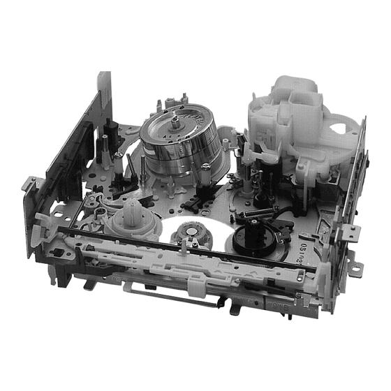
Page 35: Mecanism
MECHANISM... - Page 36 The mechanism has three motors: Drum motor (three-phase ac). - The stator of this motor is secured to the chassis. - Capstan motor - Function control motor. Functions of the Capstan Motor: - Sets the tape winding speed, - Drives the reel stands via a belt and a free wheel. Functions of the Function Control Motor: - Cassette loading and ejection, - Loading and unloading of tape,...
- Page 37 CASSETTE LOADING Microcontactor ST001 on the Main Board handles cassette detection. This microcontactor is actuated by the front left cam of the cassette holder, and closes when a cassette is inserted. The function control motor is powered, and drives the cassette holder drive axle via the cassette holder control slide and control cam.
- Page 38 REPLACEMENT OF CONTROL CAM The part references shown come from the mechanism manual. DISASSEMBLY - Remove the function control motor assembly by releasing the four clips (mechanism manual, Page 10). - Remove the cassette holder drive axle (14). - Remove the right gear of the drive axle (14) by pressing A. - Remove the drive axle (14) by pulling upwards.
- Page 39 REASSEMBLY - Place the loading arm and tape tensioning arm in unloaded tape position. - Align Guide Hole H2 of Rod 24 with the hole in the chassis. - Install the control cam by aligning its guide hole (H1) with the hole in the chassis. - Reinstall the capstan idler by inserting its control tappet in the first cam groove from the axle.
-
Page 41: Servo Control
SERVO CONTROL... - Page 43 GENERAL INFORMATION The servo control system consists mainly of microcontroller IT001: TMP90PR74. Keypad function data are generated by programming microcontroller IK01. The servo control microcontroller is continually informed about mechanism operation by the static and dynamic status data. These data allow the microcontroller to decide whether to execute or reject an order.
- Page 44 QT003 RW030 16MHz CW002 RW006 1,5Vcc TW005 RT017 AVCC1 RT018 5 VD 5 VE RW012 RW009 TW004 RW010 DW015 14 DVCC1 TW006 33 VE IT001 RW004 DVCC2 CT032 CT053 0,1F DT013 RT081 RT073 RT072 RT072 IT005 RT075 RESET CT049 + 5VE RW083 5 VS IF, RF...
- Page 45 POWER SUPPLY, CLOCK, RESET, POWER SUPPLY BACK-UP Power supplies to IT001 are obtained from the 33VE and 5 V from the power supply. A pseudo- thyristor assembly, TW005, TW004, and a transistor, TW006, allow IT001 to be powered at 5 V. - 5 VD, Pin 13 - DVCC1, Pin 14 - DVCC2, Pin 64...
- Page 46 VERSION 1 KEYBOARD CTL BUS IK01 KEYBOARD FUNCTIONS TIMER IT001 K DATAS SERVO CONTROL REMOTE CONTROL CODE IR/RECEPT. VERSION 2 KEYBOARD CTL BUS IK01 KEYBOARD FUNCTIONS TIMER IT001 K DATAS SERVO CONTROL REMOTE CONTROL CODE IR/RECEPT.
- Page 47 FUNCTION DATA KEYBOARD The KEYBOARD FUNCTION keys are located between the sweep outputs of IK01 (Pins 71/72 or 18/19) and the function inputs of IK01 (Pins 67 through 70 or 9 through 12). The keyboard function data are sent to servo control microcontroller IT001 via Output 21 or 25 of IK01.
- Page 48 CAPSTAN FG CAPSTAN MOTOR RT048 CTL PULSES 47 IT001 CTL HEAD 25Hz / 200Hz IT001 RT001 IT003 DRUM FG/PG H+ 0,5Vpp GT001 H- 0,5Vpp 5Vpp TU REEL FG 5Vpp SUPPLY REEL FG TAPE END GT005 TAPE START GT003 GT006 GT004 RT027 TT 003 12,6VE...
- Page 49 STATUS DATA - STATIC IT001 DATA COMMENTS PINS CASSETTE AND RECORDING 5 V without cassette 0 V with cassette tab off PROTECTIO MICROCONTACT 0 V cassette loading TAPE START 0 V at tape start TAPE END 0 V at tape end Indicate cassette presence...
- Page 50 GT005 TAPE END TAPE START GT006 TT 003 12,6VE ON: 5V GT002 CASSETTE IT002 MOTOR INTERFACE RT012 CASSETTE DETECT. REC. SAVE ST001 STATES TABLE IT002 IT001 CAM C STOP FORWARD REVERSE CAM B CAM A...
- Page 51 FUNCTION CONTROL MOTOR The function control motor performs the following functions: - Cassette loading and ejection, - Tape loading and unloading, - Positioning of the mechanism parts. CASSETTE LOADING Cassette insertion leads to the following actions: - Closure of ST001 (cassette microcontactor), - Pin 7 of IT001 goes to 0, - Function control motor rotates forwards.
- Page 52 24 ms 16 ms NORMAL CTL PULSE 16/9 CTL PULSE "N" -2,5% +2,5% 16/9 CTL PULSE "N+1" TX351 12,6 VE-LM RX353 1 Kohm TX350 SCART RX358 PULSE ACT : 5 V 1 Kohm IT001 TX352 16/9 :5 V...
- Page 53 AUTOMATIC 16/9 SWITCHING Certain products in this video recorder series can record and play cassettes in 16/9 format. To do this, the duty ratio of the recording and control pulses must be altered. The falling edge of the control pulses is shifted by ±2.5% in alternation. In Play Mode, the servo control/control circuit (IT001) detects this change, and enables Output This leads to the saturation of Transistor TGX352, and then a voltage of 6 V at 8 of the TV SCART.
-
Page 55: Programmig Osd
PROGRAMMING... - Page 56 13-45-80 5 Volts 14-64 5 Volts Strobe Reset Display Data S/K Data K/S IV001 VIDEO- PROCESSOR Reset Keyboard 9/10/15 QK 01 8MHz + 5 Volts 1-12-31-56-71 TUNER (MODULATOR according QT003 QT 002 to the version) 16MHz 32KHz IT 004 + 5 VE EEPROM...
- Page 57 PROGRAMMING AND DISPLAY The programming circuit includes the following elements: - Microcontroller IT001 used for programming, - EEPROM IT004, - Infrared receiver, - Programming keyboard, - Microcontroller IK001, which sends the signals from the keyboard and controls the display. Microcontroller IT001 Remote control signals are sent via the infrared receiver to Pin 48 of IT001.
- Page 58 IK001 MCU DISPLAY CTL 38 41 43 44 50 51 52 53 54 55 56 57 58 59 60 61 62 63 64 UH + DISPLAY GK01 UH - 28 29 30 31 32 33 34 35 36 37 38 39 40 G9 G10 G11 G12 G13 G14 49 48 47 46 45 44 43 42 41...
- Page 59 KEY DISPLAY BOARD (KDB) DISPLAY CONTROL CIRCUIT This front-panel control circuit consists of: a- Control microcontroller IK001F. This issues display commands, and relays the front- panel keyboard commands to the servo control microcontroller. Note: The control microcontroller is also the satellite receiver on certain models. b- Display GK01 BJ446GK.
- Page 60 LP081 14 D.Vcc 1 DP081 TW004 LP20 + 5 VE. TW005 TW006 64 D. Vcc 2 CT053 CP082 CP081 0,1F 1000uF 1000uF RT061 DT013 QT002 32KHz RP085 IT 001 TPO82 + 36 VE QT003 RP084 DP082 / 081 16MHz Halt CP081 /082 RP083...
- Page 61 MAINS POWER CUT In the event of a mains power cut, the video recorder continues to power the clock for 30 minutes. When a mains power cut occurs, Transistors TP082 and TP086 become saturated, and impose a low level on the collector of TP086. This signal is transmitted to Pin 49 of servo control microcontroller IT001 (POWER GOOD or microcontroller halt).
- Page 62 IV500 SYNCHRO H+V to 70 IT001 SEPARATEUR CLAMP AMPLI CV083 IX101 AMPLI SEL 1 LV401 CV404 SEL 2 DETECT CV087 IV401 IX 004 TV020 AMPLI TV402 TO MODULATOR PIN 19/AV1 IV001 MONITOR VIDEO AV2 FROM 29 IT 001 TT013 TV401 OSD VIDEO OSD MIX L PH 1...
- Page 63 ON-SCREEN DISPLAY (OSD) The servo control microcontroller provides the on-screen display. It is controlled via the STATUS key on the remote control unit. There are two possible display modes: - FULL SCREEN Mode, - MIX SCREEN Mode (OSD + video composite). The servo control microcontroller receives the HD horizontal synchronisation signal from Pin 9 of IV500 on Pin 69, and the composite synchronisation signal on Pin 70.
-
Page 65: Servo Control
SERVO CONTROL... - Page 66 CAPSTAN MOTOR HEAD DRUM CAPSTAN MOTOR 16MHz DRUM FG / PG QT003 NORMAL SPEED : 758Hz SEARCH (9) :6,8KHz GT001 15,16 7,8,9 FAST FORWARD/ IT003 REWIND :1,5 12KHz DRUM 25Hz/ MOTOR 200Hz 600Hz IT001 SIGNALS SERVO. GENERAT. OUTPUT AMPLIFIER DRUM START OSC.
- Page 67 Speed and phase servo control must be applied to the capstan and video head drum motors. FUNCTION OF DRUM SERVO CONTROL RECORDING: - 1500 rpm rotation, - Position one of the video heads at the start of a track when a frame time signal appears. Moreover, when Head 1 records the frame time signal, a reference mark is written to the servo control track to indicate the position of Video Track 1.
- Page 69 DRUM CABESTAN PHASE PHASE FUNCTION SPEED SPEED REFERENCE REFERENCE MEASUREMENT MEASUREMENT SPEED OSCILLATOR POSITION SPEED SPEED RECORD SENSOR RESET BY SENSOR OSCILLATOR SENSOR SENSOR GT001 SYNCHRO V GT001 25 Hz PLAY OSC. CONTROL PULSES PAUSE CAPSTAN MOTOR STOP SPEED CONTROL SEARCH OSCILLATOR SENSOR...
- Page 70 1,5Vc/c HEAD QT003 16MHz 25Hz/200Hz IT001 RT001 IT003 GT001 drum DRUM FG / PG RT014/015 CT014/015 0,4Vcc 25Hz/600Hz pin15: same signal with opposite phase FLIP FLOP 25Hz SYNC. IV500...
- Page 71 DRUM CONTROL SIGNALS REQUIRED - 16-MHz OSC., Pins 60 and 61 of IT001, - Speed and position sensor, Pin 47 of IT001, - Recording frame synch, Pin 70 of IT001. GENERATION OF DRUM VM A PWM (5 Vpp) signal is present on Output 100 of IT001. Its period is 24 µs. This signal is integrated by network RT014/CT014 and RT015/CT015.
- Page 72 DRUM MOTOR CONTROL CIRCUIT IT003 600Hz COUNTER SIGNAL DECODER GENERATOR CTL MOTOR OUTPUT OUTPUT OUTPUT AMPLIFIER AMPLIFIER AMPLIFIER START OSC. START STOP 6,10 0,1V RT008 CT016 RT009 4 Vcc /10 Hz IT003 pins 7,8,9 DRUM T=10ms MOTOR...
- Page 73 RECORDING CONTROL PULSES START REC. or press on INDEX 30 ms 10 ms IT001 REC. 16 ms 24 ms 2,4V SYNC. REF. VOLTAGE HEAD QT003 16MHz When Head 1 records the frame time signal, a reference mark is written on the control track. This picture-frequency (25 Hz) reference mark is obtained from the frame synch (50 Hz) at 70 of IT001.
- Page 74 NOTES...
- Page 75 CAPSTAN CONTROL The signals required for capstan control are as follows: - 16-MHz oscillator, IT001 Pins 60 and 61, - Speed sensor (magnetoresistive element), - PLAY control pulses. RECORDING PHASE AND SPEED CIRCUIT The FGA signal from a magnetoresistive element is used. It is amplified and shaped by IT001. Note: Two magnetoresistive elements are used.
- Page 76 QT003 16 MHz IT001 PEAK PEAK TRIGGER DETECT. - DETECT.+ U. REF. REWIND HEAD 4V(PB) 1V(PB) 2,4V CT026 CT025 BW006 RT042 RT041 RT043 CT023 24ms 16ms 16ms 24ms 3Vc/c...
- Page 77 PLAY PHASE CIRCUIT The oscillator and control pulses are used. The control pulses are read by the head, and then amplified and shaped by IT001. During the FAST REWIND and FORWARD functions, amplifier gain is reduced to avoid signal deformation through amplifier saturation or blockage, which would lead to errors in INDEX searching.
- Page 78 GENERATION OF CAPSTAN MOTOR V A 5 Vpp PWM signal is present on Output 99 of IT001. After integration by RT006, CT003, and RT005, CT004, this signal is sent to the capstan motor control circuit. In this circuit, it is compared to the reference voltage from Output 42 of IT001.
- Page 79 AUTOMATIC TRACKING This is based on the 25-Hz flip flop and the MF envelope. It consists of putting the maximum of the MF signal in phase with the centre of Video Track 1 (middle of the low level of the 25-Hz flip flop).
- Page 80 PAUSE, FRAME-BY-FRAME, AND SLOW MOTION During these functions, Video Heads 2 are in operation. They read only Tracks 2 (-6°). LD1 ( +6° ) N1 ( +6° ) N2 ( -6° ) LD2 ( -6° ) PAUSE When this function is requested, Microcontroller IT001 stops the capstan. A braking pulse (5 Vpp) is sent to the capstan motor.
- Page 81 FRAME-BY-FRAME AND SLOW MOTION When one of these functions is requested, Microcontroller IT001 places the capstan motor in Forward Rotation Mode for approximately 20 ms. In the next phase, Microcontroller IT001 seeks a control signal rising edge (reference Track 1). A few milliseconds after this rising edge (the exact time depends on the phase control), capstan motor braking is performed.
-
Page 83: Switching
SWITCHING... - Page 84 IX 001 V EE REC IV001 IN frontal VIDEO OUT TV020 MONITOR IV401 from 29 IT001 PB ON INSEL 2 INSEL 1 TV402 TX 350 V EE PB V EE PB MD TX351 COMMUT. IX 004 IX 003 MONITOR IT 001 DECODER to 19 AV2 V IF...
- Page 85 VIDEO SWITCHING The Audio and V ideo switching circuit consists of two SCAR T connectors, A V1 (black connector), and A V2 (blue connector), and four integrated circuits. VIDEO SWITCHES An integrated circuit, IX001, MC14052, handles video switching. At Inputs 1, 2, 4', and 5, it receives the composite video signal from Connectors A V2, A V1, from the IF V output of the video recorder , and from front panel connector A V3.
- Page 86 IX 001 Audio EE/REC. IX 002 TX204 IT001 MONITOR INSEL 1 from 29 IT001 INSEL 2 PB ON IX 002 Audio IF TX214 Audio Front AV ( AV3 ) Audio EE/PB DECODER from 27 IT001...
- Page 87 AUDIO SWITCHES Audio Switches IX001 and IX002 are created using Integrated Circuits MC14052 and MC14053, controlled via IT001. The audio switching table is identical to the video switching table. The microprocessor controls IX002 on Pin 9 and Pin 11.
-
Page 89: Video Processing
VIDEO PROCESSING... - Page 90 CV011/019 RV010/011 TV005 1Vcc Clamp to pin 13 IV001 BV003 CV083 KIL DET 0,5Vcc AMPLI IX001 COMMUT. 1,5V DETECT CLAMP DETECT. CV037 CHROMA to details enhancer circuit Vid o out SYNC. AMPLI SEP. TV020 4Vcc 0,35Vcc 0,3Vcc IV100 CV023 vers 4 de BV001 QV001 TV013...
- Page 91 LUMINANCE PROCESSING DURING RECORDING In R6000 Series video recorders, luminance processing is performed by circuit IV001, LA71500M. Pin 28 of this circuit receives the composite video signal from Pin 3 of input selector IX001. At the output of a clamp stage, the video signal is applied to Pin 35, at a stage of the AGC that reacts only to the amplitude of the synchronisation time signals.
- Page 92 from TV005 CHROMA 0,5Vcc from 3 from BV003 100mVcc IV001 WHITE CLIP CLAMP RV134 DARK CLIP 0,3cc BV001 TV014 TV008 DETAILS MAIN NON LINEAR. ENHANCER PREEMPHASIS MODULAT. PREEMPHASIS LV014/134 CV134/140 SHIFT Decoder 1/2 FH SYNC REC. from 37 from IV001 AMPLI CV013 CV008...
- Page 93 DETAIL ENHANCEMENT, PRE-EMPHASIS The luminance signal applied to Pin 26 is sent to the detail enhancement circuit. This circuit amplifies high-frequency, low-level signals. This circuit is active in Record Mode only. It then arrives at the non-linear pre-emphasis circuit. Pre-emphasis also increases high- frequency, low-level signals.
- Page 94 from TV005 CHROMA 0,5Vcc from 3 from BV003 100mVcc IV001 WHITE CLIP CLAMP RV134 DARK CLIP 0,3cc BV001 TV014 TV008 DETAILS NON LINEAR. MAIN ENHANCER PREEMPHASIS MODULAT. PREEMPHASIS LV014/134 CV134/140 SHIFT Decoder 1/2 FH SYNC REC. from 37 from IV001 AMPLI CV013 CV008...
- Page 95 FM MODULATION The luminance signal from the main pre-emphasis stage is sent to the FM modulator. The FM modulator generates a 3.8-MHz frequency for a synchronisation time signal backdrop, and a 4.8-MHz frequency for a 100% white. The colour rotation signal, applied at 66 of IV001, causes a continuous shift of the luminance signal leading to a 1/2-Fh shift of alternate tracks at the FM modulator output.
- Page 96 C SYN 12 BC100 KIL DET TC014 TC001 COL OFF 13 BC100 11 BC100 contr 4,43 MHz IC100 mode logi. Adj Filtres CONTR mode ERASE logi. GENE LC006/007 CC015/016 BELL ANTI LIMIT. ERASE MUTE FILTER TC015 BELL FILTER E / L 4,2V CC017 CC008...
- Page 97 SECAM CHROMINANCE PROCESSING DURING RECORDING The SECAM chrominance processing of R6000 Series video recorders is handled by IC100, a specialised integrated circuit. The composite video signal, output from Pin 3 of IX001, is applied to Pin 15 of IC100. The chrominance component of this signal is taken by a 4.4-MHz band pass filter.
- Page 98 CLAMP IV001 BALANCE AMPLI PREACC CONVERT BURST vers 4 de BV003 DETECT BURST IX001 5,06 GATE PAL CHROMA COMMUT. DETECT CV037 SEP. SYNC. MESECAM MESECAM Clock SUPP NTSC: 320FH 1/2 FH PAL/MESEC: 321FH SHIFT CONVERT Data 90ß RV015 PULSE 90ß GENE 36/76 BURST...
- Page 99 PAL CHROMINANCE PROCESSING DURING RECORDING The PAL chrominance processing of R6000 video recorders is handled by Integrated Circuit IV001. The block diagram opposite describes this processing. The input signal from switching circuit IX001 is applied to a clamp circuit on Pin 28 of IV001. The signal returns on Pin 35, and is sent to an AGC stage and a band pass filter with central frequency 4.3 MHz.
- Page 100 CLAMP IV001 BALANCE AMPLI PREACC CONVERT BURST vers 4 de BV003 DETECT BURST IX001 5,06 GATE PAL CHROMA COMMUT. DETECT CV037 SEP. SYNC. MESECAM MESECAM Clock SUPP NTSC: 320FH 1/2 FH PAL/MESEC: 321FH CONVERT SHIFT Data 90ß RV015 PULSE 90ß GENE 36/76 BURST...
- Page 101 CONVERTER 2 PRODUCTION OF 40 Fh + 1/8 Fh SIGNAL The 40 Fh + 1/8 Fh signal is generated from a 321-Fh (5.01 MHz) VCO. This VCO is frequency-locked by the signal output from the 321-way divider and by the line sync of the video signal to be recorded.
- Page 102 CLAMP IV001 BALANCE AMPLI PREACC CONVERT BURST vers 4 de BV003 DETECT BURST IX001 5,06 GATE PAL CHROMA COMMUT. DETECT CV037 SEP. SYNC. MESECAM MESECAM Clock SUPP NTSC: 320FH 1/2 FH PAL/MESEC: 321FH SHIFT CONVERT Data 90ß RV015 PULSE 90ß GENE 36/76 BURST...
- Page 103 CONVERTER 1 AND OUTPUT STAGE The 5.06-MHz signal is sent to the second input of Converter 1. This converter receives the 4.43-MHz +0.6/-0.8 incident signal at its other input, and outputs two frequencies: The sum of two frequencies: 5.06 MHz + (4.43 MHz + 0.6/-0.8) and the difference between two frequencies: 5.06 MHz - (4.43 MHz + 0.6/-0.8) The difference component, 626,953 kHz -600/+800, is selected by a low pass filter with a cutoff...
- Page 104 to 15 from IV001 imput PB Color PAL/ MESECAM / NTSC IV001 LV072 LV073 CV071 CV075 BV001 TV001CVOO5 0,4Vcc TV004 LV070- LV071-LV001 TV003 TV070 DOUBLE DEMOD AMPLI MF EQUALIZER AMPLI LIMITOR 627KHz 1,1MHz from COMPAR DROP PREAMP DFFHASEL DETECTOR CV037 RV098 RV039 RV099...
- Page 105 PLAYBACK PREAMPLIFIER The preamplifier is built into the fixed part of the drum motor. It receives and issues the following signals: • BV001 Pin 8: Y FM and chroma signal, • BV001 Pin 7: comparator signal, used for standard speed search and giving the level of the signal read by head pair SP1/LP2 or SP2/LP1, •...
- Page 106 to 15 from IV001 imput PB Color PAL/ MESECAM / NTSC IV001 LV072 LV073 CV071 CV075 BV001 TV001CVOO5 0,4Vcc TV004 LV070- LV071-LV001 TV003 TV070 DOUBLE DEMOD AMPLI MF EQUALIZER AMPLI LIMITOR 627KHz 1,1MHz from COMPAR DROP PREAMP DFFHASEL DETECTOR CV037 RV098 RV039 RV099...
- Page 107 LUMINANCE PROCESSING DURING PLAYBACK The signal sent out by the playback preamplifier board is available on Pin 8 of Connector BV001. T wo traps, 627-kHz for P AL and 1.1 MHz for SECAM, eliminate the chroma. The luminance is sent to a correction amplifier . This circuit corrects the response curve of the play heads, so that a linear response is obtained whatever the signal frequency deviation.
- Page 108 CHROMA PB from 10 BV003 76 IT001 IV001 from TC005 CLAMP MUTE DROP SHARPNESS DETECTOR AMPLI AMPLI NOISE DESEMPHASIS REDUCT. CLAMP 0,3Vcc 0,35Vcc CV023 vid o output TV013 TV020 QV001 4,43MHz IV100 DELAY...
- Page 109 YNR AND DROPOUT DETECTION The signal that arrives at IV001 Pin 26 is sent to a switch. The output of this switch is connected to the input of a CCD delay circuit (IV100) and the noise reduction stage. This circuit delays the luminance channel by one line. The delayed channel is reinjected at 40 of IV001, and adjusted to the correct level by an AGC.
- Page 110 TC014 KIL DET 13 BC100 C SYN TC001 COL OFF 12 BC100 11 BC100 CONTR IC100 4,43 MHz mode Adj Filtres logi. ERASE LC003 GENE CC014 AMPLI Bell Anti MUTE TC003 filter bell LIMIT. ERASE LECT filter E / L 4,2V CC010 CC017...
- Page 111 SECAM CHROMINANCE PROCESSING DURING PLAYBACK The signal from the playback preamplifier board is available on Pin 8 of Connector BV001, and Pin 1 of connector BC100. The chrominance component of this signal is taken by the 1.1-MHz band pass filter incorporated in IC100.
- Page 112 IV100 MESEC 0,2Vcc IV001 0,4Vcc DELAY 0,2Vcc BALANCE RV223 to 9 BV003 PAL/NTSC CCD DELAY TV003 NTSC MESEC 0,2Vcc BURST CONVERT 2FSC BV001 CCD DELAY 4,43MHz from DESEMPHASIS TV004 0,4Vcc PREAMP PAL/NTSC 0,4Vcc NTSC 5,06 59 de IV001 RV007 RV005 PAL/SECAM CHROMA DET.
- Page 113 PAL CHROMINANCE PROCESSING DURING PLAYBACK The block diagram opposite describes this processing. The input signal, sent from Pin 8 of Connector BV001, is amplified and injected at 15 of IV001. A low-pass filter with cutoff frequency 1.4 MHz selects the PAL chroma component. ACC STAGE The ACC used for playback is the same as that used for recording.
- Page 114 MESEC IV100 0,2Vcc IV001 0,4Vcc DELAY BALANCE 0,2Vcc RV223 to 9 BV003 PAL/NTSC CCD DELAY TV003 MESEC NTSC BURST CONVERT 0,2Vcc 2FSC BV001 CCD DELAY 4,43MHz from DESEMPHASIS TV004 0,4Vcc PAL/NTSC PREAMP 0,4Vcc NTSC 5,06 59 de IV001 RV005 RV007 PAL/SECAM CHROMA DET.
- Page 115 CONVERTER 2 PRODUCTION OF 40 Fh + 1/8 Fh signal. The 40 Fh + 1/8 Fh signal is generated based on a 321 Fh (5.01 MHz) VCO. To ensure that the converter output signal is perfectly in phase with the playback signal, the VCO frequency is controlled by the error voltage output by a phase detector.
- Page 116 MESEC IV100 0,2Vcc IV001 0,4Vcc DELAY BALANCE 0,2Vcc RV223 to 9 BV003 PAL/NTSC CCD DELAY TV003 MESEC NTSC BURST CONVERT 0,2Vcc 2FSC BV001 CCD DELAY 4,43MHz from DESEMPHASIS TV004 0,4Vcc PAL/NTSC PREAMP 0,4Vcc NTSC 5,06 59 de IV001 RV005 RV007 PAL/SECAM CHROMA DET.
- Page 117 CONVERTER 1 AND OUTPUT STAGE The 5.06-MHz signal is sent to the second input of Converter 1. This converter receives the 626,953-kHz incident signal at its other input, and outputs two frequencies: The sum of two frequencies: 5.06 MHz + (626,953 kHz +800/-600) and the difference between two frequencies: 5.06 MHz - (626,953 kHz +800/-600) The difference component is selected by a low pass filter and is available at Outputs 48 and 50...
- Page 118 1.3 Service Einstellungen 1.3 Service Adjustments 1.3.1 Einrichten der Bedienteil-Software 1.3.1 KDB Software Set-Up Es ist notwendig den KDB-Prozessor über die bestehende l t i s n e c e s s a r y to inform t h e K D B processor which Hardware-Konfiguration zu informieren.
- Page 119 Number of digit Meaning Value Brand Thomson 1 - Nordmende Ferguson (Thomson) Thomson (ASIA) Telefunken Saba Brandt Ferguson (Saba) 8 - GE (Australia) Tuner Sound 0 - L (4.5 MHz AM) 1 - BG (5.5 MHz FM) (6 MHz FM) DKK’(6.5 MHz FM)
- Page 120 2.2 Einrichten der Video-Signalverarbeitung 2.2 Installation of the Video Signal processing i n d e r F a b r i k a u t o m a t i s c h Die Geräte werden The sets are adjusted automatically in the factory. The abgeglichen.
- Page 121 Number of the digit Meaning Value Example 1 and 2 Playback Equalizer bit O-l PB EQ GAIN (OO:min 1l:max) bit 2-3 PB EQ 2 Alwavs 0 bit O-2 REC C (OOO:max PB Noise Canceller 0 = Off 1 = on REC C Level (OOO:max attn 111: min attn) Description of digits used for the Video Signal processing setup.
- Page 122 2.4 Power Supply 9 Alimentation = Netzteil Einstellung Betriebs- Meßmittel Meßpunkt Einstell- Beschreibung Eingangssignal Punkt Mode & Test Equipment Testpoint Adjustment Item Description Sianal Point DC supply 2.4.1 Main board BW001 voltage Standby None Hauptleiterplatte BW001 pin 112 pin 3 2,0 v pin 4 Voltmeter...
- Page 123 2.6 Measurements Servo part - Main board Messungen Servoteil - Hauptleiterplatte high level > 4.0 V Anmerkung: Note: low level < 0.8 V; L-Pegel < 0,8 Volt; H-Pegel > 4,0 Volt Einstellung Betriebs- Meßmittel Meßpunkt Beschreibung Eingangssignal Punkt Item Mode & Test Equipment Testpoint Adjustment Description Signal...
- Page 124 2.7 IF circuit - Fl - ZF-Modul Einstellung Betriebs- Meßmittel Meßpunkt Beschreibung Eingangssignal Punkt Mode & Test Equipment Item Testpoint Adjustment Description Sianal Point E-E, RF Voltmeter IF Input Pl 20 inside 1. Maximum Tuner Generator IF box 2. -10 dB 3mV / CH09 E-E, HF-Voltmeter,...
- Page 125 Abbreviations / Abreviations I Abkürzungen Serial Glock High Pass Filter Infra Red Serial Data SECAM SU REEL Supply Reel Input Key Display Board SMPS Switch Mode Power Supply Standard Play Limitter Synch Separator Long Play Low Pass Filter Switch TU REEL Take Up Reel Middle East Secam MESECAM...
- Page 126 POWER SUPPLY INTERFACE / TUNER / IF SECTION - INTERFACE ALIMENTATION / TUNER / FI - NETZEIL INTERFACE / TUNER / ZF - ALIMENTAZONE / TUNER / IF - INTERFAZ ALIMENTACIÒN / TUNER / IF SCHEMATIC DIAGRAM - SCHEMA DE PRINCIPE - SCHALTBILD - SCHEMA - ESQUEMA RS035 LS030 LS002...
- Page 127 MEASUREMENTS POWER SUPPLY INTERFACE / TUNER / IF SECTION - MESURES INTERFACE ALIMENTATION / TUNER / FI - MESSUNGEN NETZEIL INTERFACE / TUNER / ZF - MISURE INTERFACCIA ALIMENTAZIONE / TUNER / IF - MEDIDAS INTERFAZ ALIMENTACIÒN / TUNER / IF TU / IF MODE TU / IF...
- Page 128 VIDEO SIGNAL PROCESSING - TRAITEMENT LUMINANCE / CHROMINANCE - VIDEO SIGNALVERARBEITUNG - ELABORAZIONE VIDEO - TRATAMIENTO VIDEO SCHEMATIC DIAGRAM - SCHEMA DE PRINCIPE - SCHALTBILD - SCHEMA - ESQUEMA JV075 RV054 JV073 JV170 JV149 JV162 JV138 RV059 JV061 JV116 +5VS JV160 JV120 +5VS...
- Page 129 MEASUREMENTS VIDEO SIGNAL PROCESSING - MESURES TRAITEMENT VIDEO - MESSUNGEN VIDEO SIGNALVERARBEITUNG - MISURE ELABORAZIONE VIDEO - MEDIDAS TRATAMIENTO VIDEO VIDEO MODE VIDEO MODE VIDEO MODE PLAY REC. PLAY REC. PLAY REC. DV401 TV001 IV001 TV002 IV001 pin15-20 IV001 pin37 IV001 pin17 IV001 pin25 TV003...
- Page 130 MECHA DECK CONTROL / SERVO CONTROL - GESTION / ASSERVISSEMENTS - MECHANIKSTEUERUNG / SERVO - CONTROLLO MECCANICA / SERVO - SERVOMECANISMO / GESTIÒN SCHEMATIC DIAGRAM - SCHEMA DE PRINCIPE - SCHALTBILD - SCHEMA - ESQUEMA JT087 JT022 JT007 JT222 JT290 RT013 OSD_MIX_L JT026...
- Page 131 MEASUREMENTS MECHA DECK CONTROL / SERVO CONTROL - MESURES GESTION / ASSERVISSEMENTS - MESSUNGEN MECHANIKSTEUERUNG / SERVO - MISURE CONTROLLO MECCANISMO - MEDIDAS SERVOMECANISMO / GESTION SERVO MODE IT001 pin33 SERVO MODE SERVO MODE IT001 pin35 SP PB IT001 pin36 FF-REW IT001 pin40-44 SP PB...
- Page 132 Main P.C.B. components side - Circuit imprimé de la platine principale côté composants - Hauptleiterplatte Bestückungsseite - Piastra principale lato componenti - Platina principal lado componentes...
- Page 133 Main P.C.B. Solder side • Circuit imprimé de la platine principale côté cuivre • Hauptleiterplatte Lötseite Piastra principale lato saldature • Platina principal lado del cobre...
- Page 134 COMPONENTS LOCATION - LOCALISATION DES ELEMENTS - LAGE DER BAUTEILE JV068* D4 JX100 LZ005 RP029* L6 RT044* I4 RV070* D5 RX210* H8 TP082* L3 JV073* C8 JX101* J7 LZ006 RV071* C4 RX214* J6 TP086* K3 RP031 RT045* I4 LOCALIZZAZIONE DEI COMPONENTI - LOCALIZACION DE LOS COMPONENTS JV074* C8 JX102* J6 LZ011...
- Page 135 20 296280 G480 MECHANISM 1 / MECANIQUE 1 / MECHANIK 1 / MECCANISMO 1/ MECANICA 1 R : RECYCLED PART For any requests, please contact THOMSON multimedia after sales service area 06 / 97 35044020 : PIECE RECYCLEE Pour toutes précisions, contactez votre service apres vente local THOMSON multimedia REV.
- Page 136 20 1865 10 2 018 809 0 2 0 1 8 6 6 3 0 2 01 88 55 0 G420 K490 G450 K570 2 0 1 87 5 4 0 K530 2 0 1 88 5 2 0 K550 2 0 1 86 8 4 0 K252 2 0 3 92 3 7 0...
- Page 137 En efecto, en bien de la calidad de nuestros productos, nos reservamos el derecho de efectuar, sin previo aviso, cualquier modificación o mejora. THOMSON multimedia S.A au capital de 4 594 812 200 FF - 46, Quai Alphonse Le Gallo 92648 Boulogne Cedex FRANCE - RCS NANTERRE B 333 773 174...
- Page 139 Documentation technique exclusivement destinée aux professionnels de la maintenance...