Sony HT-CT180 Service Manual
Active speaker system/sound bar
Hide thumbs
Also See for HT-CT180:
- Operating instructions manual (71 pages) ,
- Startup manual (2 pages) ,
- Operating instructions manual (28 pages)
Table of Contents
Advertisement
SERVICE MANUAL
Ver. 1.0 2015.02
• All of the units included in the HT-CT180
(SA-CT180/SA-WCT180/Remote control)
are required to confi rming operation
of SA-CT180. Check in advance that
you have all of the units.
Note:
Be sure to keep your PC used for service and
checking of this unit always updated with the
latest version of your anti-virus software.
In case a virus affected unit was found during
service, contact your Service Headquarters.
COMPONENT MODEL NAME
Bar Speaker (Active Speaker System)
Subwoofer (Active Subwoofer)
• Please refer to service manual separately issued for Subwoofer.
Amplifier section
U.S. models:
POWER OUTPUT AND TOTAL HARMONIC
DISTORTION:
(FTC)
Front L + Front R:
With 4 ohms loads, both channels
driven, from 200 Hz - 20,000 Hz; rated
13 Watts per channel minimum RMS
power, with no more than 1% total
harmonic distortion from
250 milliwatts to rated output.
POWER OUTPUT (reference)
Front L/Front R speaker:
25 Watts (per channel at 4 ohms,
1 kHz)
Except US models:
POWER OUTPUT (rated)
Front L + Front R:
13 W + 13 W (at 4 ohms, 1 kHz, 1% THD)
POWER OUTPUT (reference)
Front L/Front R speaker:
25 Watts (per channel at 4 ohms,
1 kHz)
Inputs
OPTICAL
ANALOG
9-896-127-01
Sony Corporation
2015B33-1
©
2015.02
Published by Sony Techno Create Corporation
HT-CT180
SA-CT180
SA-WCT180
SPECIFICATIONS
BLUETOOTH section
Communication system
BLUETOOTH Specification version 4.0
Output
BLUETOOTH Specification Power Class
2
Maximum communication range
1)
Line of sight approx. 10 m (33 ft)
Maximum number of devices to be
registered
8 devices
Frequency band
2.4 GHz band (2.4000 GHz -
2.4835 GHz)
Modulation method
FHSS (Freq Hopping Spread Spectrum)
2)
Compatible BLUETOOTH profiles
A2DP (Advanced Audio Distribution
Profile)
3)
Supported Codecs
4)
SBC
Transmission range (A2DP)
20 Hz - 20,000 Hz (Sampling frequency
44.1 kHz)
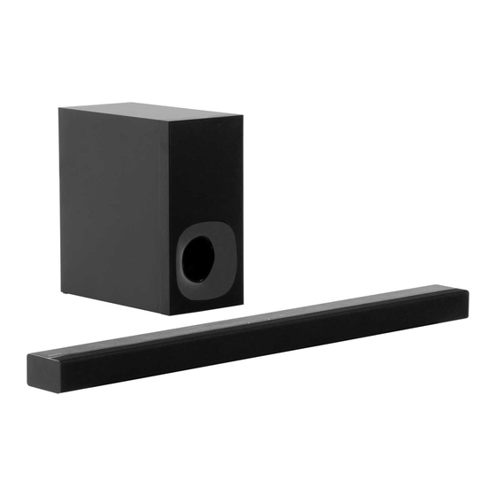
HT-CT180
Photo: SA-CT180
1)
The actual range will vary depending on
factors such as obstacles between
devices, magnetic fields around a
microwave oven, static electricity,
cordless phone, reception sensitivity,
operating system, software application,
etc.
2)
BLUETOOTH standard profiles indicate
the purpose of BLUETOOTH
communication between devices.
3)
Codec: Audio signal compression and
conversion format
4)
Subband Codec
Speakers
Front L/Front R speaker section
Speaker system
2-way speaker system, Acoustic
suspension
Speaker
9
Tweeter: 14 mm - 25 mm (
/
in - 1 in)
16
balance dome type
5
Woofer: 40 mm × 120 mm (1
/
in ×
8
3
4
/
in) cone type
4
ACTIVE SPEAKER SYSTEM
SA-CT180
US Model
Canadian Model
AEP Model
UK Model
Australian Model
General
Power requirements
120 V AC, 60 Hz (US and Canadian models)
220 V - 240 V AC, 50 Hz/60 Hz
(AEP, UK and Australian models)
Power consumption
On: 17 W
Standby mode: 0.5 W or less
BLUETOOTH Standby mode: 3 W or
less
Dimensions (approx.) (w/h/d)
901 mm × 52 mm × 84 mm
1
1
3
(35
/
in × 2
/
in × 3
/
in)
2
8
8
Mass (approx.)
2 kg (4 lb 7 oz)
Wireless transmitter
Frequency band
2.4 GHz band (2.404 GHz - 2.476 GHz)
Modulation method
GFSK
Supplied accessories
Remote control (1)
R03 (size AAA) batteries (2)
Optical digital cable (1)
Speaker pads for the subwoofer (4)
Design and specifications are subject to
change without notice.
HT-CT180
SOUND BAR
SA-CT180
Advertisement
Table of Contents

Related Manuals for Sony HT-CT180


Summary of Contents for Sony HT-CT180
-
Page 1: Specifications
Canadian Model Ver. 1.0 2015.02 AEP Model UK Model Australian Model • All of the units included in the HT-CT180 (SA-CT180/SA-WCT180/Remote control) are required to confi rming operation of SA-CT180. Check in advance that you have all of the units. - Page 2 THESE COMPONENTS WITH SONY PARTS PAR DES PIÈCES SONY DONT LES NUMÉROS SONT DON- WHOSE PART NUMBERS APPEAR AS SHOWN IN THIS NÉS DANS CE MANUEL OU DANS LES SUPPLÉMENTS MANUAL OR IN SUPPLEMENTS PUBLISHED BY SONY. PUBLIÉS PAR SONY.
-
Page 3: Table Of Contents
4-9. Printed Wiring Board - KEY Board -......25 ERATION 4-10. Schematic Diagram - KEY Board - ........ 25 All of the units included in the HT-CT180 (SA-CT180/SA- 4-11. Schematic Diagram - BT NFC Board - ......26 WCT180/Remote control) are required to confi rming operation of 4-12. -
Page 4: Model Identification
HT-CT180 MODEL IDENTIFICATION Distinguish by Part No. on the bottom side of a main unit. Note: The printed contents of following fi gure model number label may be different from the model number label of a main unit. MODEL NUMBER LABEL... -
Page 5: Enabling Secure Link Function
HT-CT180 ABOUT PARTS REPAIR OF EACH BOARDS METHOD OF RESET When each boards installed in this unit are defective, individual If the system still does not operate electrical parts that the mount is done cannot be replaced. When properly, reset the system as follows:... -
Page 6: Disassembly
HT-CT180 SECTION 2 DISASSEMBLY • This set can be disassembled in the order shown below. 2-1. DISASSEMBLY FLOW 2-2. REAR CABINET BLOCK (Page 7) 2-3. AC CORD (AC1) (Page 8) 2-4. MAIN BOARD BLOCK 2-6. NFC MODULE (Page 9) (Page 11) 2-5. -
Page 7: Rear Cabinet Block
HT-CT180 Note: Follow the disassembly procedure in the numerical order given. 2-2. REAR CABINET BLOCK 4 rear cabinet block Right side 3 KEY board cable connector (XP3) 1 thirteen screws 2 Lift up the rear cabinet 10 B) block in the direction of the arrow. -
Page 8: Ac Cord (Ac1)
HT-CT180 2-3. AC CORD (AC1) cord bush 2 claw 2 claw – Front cabinet rear view – 1 AC cord connector (CN501) Bottom side Left side 4 AC cord block Top side Note 1: Please spread a sheet under a unit not to injure front cabinet. -
Page 9: Main Board Block
HT-CT180 2-4. MAIN BOARD BLOCK 7 antenna wire terminal 3 two screws Right side 5 FFC 22P (FFC2) 8 S) (XS1) 9 MAIN board block 6 R-ch speaker cable connector (XP11) How to install the flexible flat cable When installing the flexible flat cable,... -
Page 10: Main Board
HT-CT180 2-5. MAIN BOARD 2 WIRELESS board Note 1: When WIRELESS board is replaced, refer to “NOTE OF REPLACING THE WIRELESS BOARD” on page 5. 4 cushion (A) (See Fig. A) 7 four screws 6 B) 5 cushion (B) (See Fig. A) -
Page 11: Nfc Module
HT-CT180 2-6. NFC MODULE Note 1: When replacing the BT NFC board or the NFC module, be sure to replace both at the same time. The BT NFC board or the NFC module cannot replace with single. 2 screw 1 connector... -
Page 12: Antenna (Ant1)
HT-CT180 2-8. ANTENNA (ANT1) Note 2: Pass the antenna wire between the loudspeaker three grooves groove three grooves and the front cabinet block. antenna wire tweeter woofer (L-ch) (L-ch) Right side 1 Peel off the adhesive sheet. Note 1: Please spread a sheet under a unit 2 antenna not to injure front cabinet. -
Page 13: Loudspeaker (Sp1, Sp3) (L-Ch)
HT-CT180 2-9. LOUDSPEAKER (SP1, SP3) (L-CH) Note 2: Pass the speaker cord terminal terminal over the top of the (wide side) (narrow side) loudspeaker (SP2). [red] [black] 2 speaker cord 1 terminal (narrow side) 1 terminal [black] (wide side) [red]... -
Page 14: Bt Nfc Board
HT-CT180 2-10. BT NFC BOARD Note 1: When replacing the BT NFC board or the NFC module, be sure to replace both at the same time. The BT NFC board or the NFC module cannot replace with single. tweeter Top side... -
Page 15: Loudspeaker (Sp2, Sp4) (R-Ch)
HT-CT180 2-11. LOUDSPEAKER (SP2, SP4) (R-CH) Note 2: Pass the speaker cord over the top of the terminal terminal loudspeaker (SP2). (narrow side) (narrow side) [black] [black] loudspeaker terminal terminal loudspeaker (SP4) (wide side) (wide side) (SP2) Insert the speaker terminal straight into the interior. -
Page 16: Test Mode
HT-CT180 SECTION 3 TEST MODE VERSION DISPLAY DEMO MODE The check of the software version can be performed. The demo mode can be performed. (This mode is used by shop front) Procedure: 1. Press the [ ] button to turn the power on. -
Page 17: Diagrams
HT-CT180 SECTION 4 DIAGRAMS 4-1. BLOCK DIAGRAM Wireless Module IA2S4M Optical In AUDIO_IN TAS3157*2 AK5358 TBM- IIC2 C830 REST MCLK MCLK 25W THD 30% 25W THD 30% BCLK2 DATA3 BCLK LRCLK2 LRCLK DATA1 BCLK1 MCLK MCLK LRCLK1 LRCLK1 Audio NFC-FS2... - Page 18 HT-CT180 THIS NOTE IS COMMON FOR PRINTED WIRING BOARDS AND SCHEMATIC DIAGRAMS. • Circuit Boards Location (In addition to this, the necessary note is printed in each block.) For Printed Wiring Boards. For Schematic Diagrams. Note: Note: • All capacitors are in μF unless otherwise noted. (p: pF) 50 •...
-
Page 19: Printed Wiring Board - Main Board
HT-CT180 4-2. PRINTED WIRING BOARD - MAIN Board - • See page 18 for Circuit Boards Location. • : Uses unleaded solder. MAIN BOARD (COMPONENT SIDE) MAIN BOARD (CONDUCTOR SIDE) HT-CT180... -
Page 20: Schematic Diagram - Main Board (1/6)
HT-CT180 4-3. SCHEMATIC DIAGRAM - MAIN Board (1/6) - • See page 28 for IC Block Diagrams. MAIN BOARD (1/6) KBP306 KBP306 LIF4-22-15 LIF4-22-15 R502C R502C 470pF/250VAC 470pF/250VAC R502A R502A CY502 CY502 LIF501 LIF501 FB504 FB504 FB90@100MHz FB90@100MHz CE502 CE502... -
Page 21: Schematic Diagram - Main Board (2/6)
HT-CT180 4-4. SCHEMATIC DIAGRAM - MAIN Board (2/6) - • See page 28 for IC Block Diagrams. MAIN BOARD (2/6) STB_3V3 POWER_18V AMP_VCC Rate : 2A 30V 160m 340KHz TP43 TP43 In Range: 4-30V Out Range: 0.923V-12V POWER_ON POWER_18V NPN_3DG3904M NPN_3DG3904M Vout=0.923(R1+R2/R2) -
Page 22: Schematic Diagram - Main Board (3/6)
HT-CT180 4-5. SCHEMATIC DIAGRAM - MAIN Board (3/6) - • See page 28 for IC Block Diagrams. • See page 29 for IC Pin Function Description. MAIN BOARD (3/6) A_1V2 150mA 500/500mA 500/500mA A_1V2 MTK_DATA0 => L, R C808 C808... -
Page 23: Schematic Diagram - Main Board (4/6)
HT-CT180 4-6. SCHEMATIC DIAGRAM - MAIN Board (4/6) - • See page 28 for IC Block Diagrams. MAIN BOARD (4/6) Vref2v5 Vref2v5 Vref2v5 100K 100K FB615 FB615 500/200mA 500/200mA MP3_L R410 R410 R411 R411 R406 R406 R405 R405 STB_3V3 FB616... -
Page 24: Schematic Diagram - Main Board (5/6)
HT-CT180 4-7. SCHEMATIC DIAGRAM - MAIN Board (5/6) - • See page 29 for IC Pin Function Description. MAIN BOARD (5/6) +3.3VD PNP_MMBT8550C PNP_MMBT8550C LL4148 LL4148 STB_3V3 CE13 CE13 47uF/SMD 47uF/SMD FB33 FB33 NC/500/500mA NC/500/500mA BT_PIO7 R166 R166 NC/33 NC/33... -
Page 25: Schematic Diagram - Main Board (6/6)
HT-CT180 4-8. SCHEMATIC DIAGRAM - MAIN Board (6/6) - MAIN BOARD (6/6) STB_3V3 C277 "18PF/5%" C277 "18PF/5%" STB_3V3 R217 R217 4.7K 4.7K R143 R143 BAT54S BAT54S R139 R139 C458 C458 TP60 TP60 NFC_INT NC/100K NC/100K NFC_INT BT_NFC NC/15PF NC/15PF R136... -
Page 26: Schematic Diagram - Bt Nfc Board
HT-CT180 4-11. SCHEMATIC DIAGRAM - BT NFC Board - BT NFC BOARD Bluetooth 10K/1% 10K/1% R938 R938 R945 R945 R946 R946 10K/1% 10K/1% C793 C793 R937 R937 4.7UF/10V/X5R 4.7UF/10V/X5R C797 C797 10uF 10uF R224 R224 BT_R1 R949 R949 10K/1% 10K/1%... -
Page 27: Printed Wiring Board - Bt Nfc Board
HT-CT180 4-12. PRINTED WIRING BOARD - BT NFC Board - 4-13. PRINTED WIRING BOARD - LED Board - • See page 18 for Circuit Boards Location. • : Uses unleaded solder. • See page 18 for Circuit Boards Location. •... - Page 28 HT-CT180 • IC Block Diagrams – MAIN Board – U11 AK5358A U2, 3 EUP3482ADIR1 U21, 22 74LVC1G3157GV U4 AS1117 U531 TOP256EN U5 M12L64164A-7T Clock Generator Bank D Bank C Bank B Address Address Buffer Bank A Mode & Register Refresh...
- Page 29 HT-CT180 • IC Pin Function Description MAIN BOARD U6 MT8301_OQE (SYSTEM CONTROLLER) Pin No. Pin Name Description AVDD12_2 Power supply terminal (+1.2V) AVDD33_1 Power supply terminal (+3.3V) XTALI System clock input terminal (27 MHz) XTALO System clock output terminal (27 MHz) Reference voltage (+1.4V) input terminal...
- Page 30 HT-CT180 Pin No. Pin Name Description 77 to 81 RA10, RA0 to RA3 Address signal output terminal (for SDRAM) DVDD12 Power supply terminal (+1.2V) SPDIF/GPIO12 Power on/off control signal output terminal GPIO10/HPLG Bluetooth pairing key input terminal EXT_RES External resistor connection terminal AVDD33_12 Power supply terminal (+3.3V)
- Page 31 HT-CT180 MAIN BOARD U14 STA339BW (DIGITAL AMP) Pin No. Pin Name Description GND_SUB Ground terminal I2C select address signal input terminal Fixed at “L” in this unit TEST_MODE Fixed at “L” in this unit Internal reference voltage (–3.3V) input/output terminal...
-
Page 32: Exploded Views
HT-CT180 SECTION 5 EXPLODED VIEWS Note: • -XX and -X mean standardized parts, so • The mechanical parts with no reference The components identifi ed by mark 0 they may have some difference from the number in the exploded views are not sup- or dotted line with mark 0 are critical for original one. -
Page 33: Front Cabinet Section
HT-CT180 5-2. FRONT CABINET SECTION (CUSHION (A)) (CUSHION (B)) (CUSHION (EVA)) (CUSHION (C)) not supplied ANT1 (SHEET (IC)) (CUSHION (C)) FFC1 not supplied NFC module not supplied FFC2 not supplied BT NFC board Note 1: When replacing the BT NFC board or the NFC module, be sure to replace both at the same time. -
Page 34: Accessories
HT-CT180 SECTION 6 ACCESSORIES Ref. No. Part No. Description Remark 4-559-026-11 MANUAL, INSTRUCTION (ENGLISH, FRENCH, SPANISH) (US, CND) 4-559-026-21 MANUAL, INSTRUCTION (ENGLISH) (UK, AUS) 4-559-026-31 MANUAL, INSTRUCTION (FRENCH, SPANISH, DUTCH) (AEP) 4-559-026-41 MANUAL, INSTRUCTION (GERMAN, POLISH, ITALIAN) (AEP) 4-569-356-11 MANUAL, INSTRUCTION (SWEDISH) (AEP) - Page 35 HT-CT180 MEMO...
-
Page 36: Revision History
HT-CT180 REVISION HISTORY Ver. Date Description of Revision 2015.02...