Table of Contents
Advertisement
Quick Links
Telephone Equipment
KX-TG3531BXS
KX-TG3531BXB
KX-TG3532BXS
KX-TG3532BXB
KX-TGA351BXS
KX-TGA351BXB
2.4 GHz Expandable Digital Cordless
Answering System
Silver Version
Black Version
(for Asia, Middle Near East and Other areas)
© 2007 Panasonic Communications Co., Ltd. All
rights reserved. Unauthorized copying and distribu-
tion is a violation of law.
ORDER NO. KM40611246CE
Advertisement
Table of Contents
Troubleshooting

Related Manuals for Panasonic KX-TG3531BXS


Summary of Contents for Panasonic KX-TG3531BXS
- Page 1 KX-TGA351BXS KX-TGA351BXB 2.4 GHz Expandable Digital Cordless Answering System Silver Version Black Version (for Asia, Middle Near East and Other areas) © 2007 Panasonic Communications Co., Ltd. All rights reserved. Unauthorized copying and distribu- tion is a violation of law.
- Page 2 KX-TG3531BXS/KX-TG3531BXB/KX-TG3532BXS/TG3532BXB/KX-TGA351S/KX-TGA351B...
-
Page 3: Table Of Contents
KX-TG3531BXS/KX-TG3531BXB/KX-TG3532BXS/TG3532BXB/KX-TGA351S/KX-TGA351B TABLE OF CONTENTS PAGE PAGE 1 Safety Precaution ------------------------------------------------ 4 13.7. Schematic Diagram (Charger Unit)------------------ 91 1.1. For Service Technicians --------------------------------- 4 14 Printed Circuit Board ------------------------------------------ 93 2 Warning -------------------------------------------------------------- 4 14.1. Circuit Board (Base Unit_Main) ---------------------- 93 2.1. -
Page 4: Safety Precaution
KX-TG3531BXS/KX-TG3531BXB/KX-TG3532BXS/TG3532BXB/KX-TGA351S/KX-TGA351B 1 Safety Precaution 1.1. For Service Technicians ICs and LSIs are vulnerable to static electricity. When repairing, the following precautions will help prevent recurring malfunctions. 1. Cover plastic parts boxes with aluminum foil. 2. Ground the soldering irons. 3. Use a conductive mat on worktable. -
Page 5: Specifications
KX-TG3531BXS/KX-TG3531BXB/KX-TG3532BXS/TG3532BXB/KX-TGA351S/KX-TGA351B 2.2.1. Suggested PbF Solder There are several types of PbF solder available commercially. While this product is manufactured using Tin, Silver, and Copper (Sn+Ag+Cu), you can also use Tin and Copper (Sn+Cu), or Tin, Zinc, and Bismuth (Sn+Zn+Bi). Please check the manufac- turer’s specific instructions for the melting points of their products and any precautions for using their product with other materi-... -
Page 6: Technical Descriptions
KX-TG3531BXS/KX-TG3531BXB/KX-TG3532BXS/TG3532BXB/KX-TGA351S/KX-TGA351B 4 Technical Descriptions 4.1. FHSS Description 4.1.1. Frequency The frequency range of 2.4 GHz - 2.48 GHz is used. Transmitting and receiving channel between Base Unit and Handset is same frequency. Refer to Frequency Table (P.81). 4.1.2. FHSS (Frequency Hopping Spread Spectrum) This telephone is using an IC chip which has similar specification to WDCT (World Digital Cordless Telephone) and is the tele- phone system that can use multiple portable unit simultaneously. - Page 7 KX-TG3531BXS/KX-TG3531BXB/KX-TG3532BXS/TG3532BXB/KX-TGA351S/KX-TGA351B 4.1.2.1. TDD Frame Format Sync Field (72bit): Preamble 56bit + SyncWord 16bit Base Unit (Handset) adjusts the timing of reception so that reception of Base Unit (Handset) can correspond to transmission of Handset (Base Unit). It is necessary for sync-field that Handset gets synchronization.
- Page 8 KX-TG3531BXS/KX-TG3531BXB/KX-TG3532BXS/TG3532BXB/KX-TGA351S/KX-TGA351B 4.1.3. Signal Flowchart in the Whole System Reception CN101 of the Base Unit is connected to the TEL line, and signal is entered through the bridge diode D101. While talking, the relay (Q141) is turned ON and amplified at the Q171, then led to DSP (IC501). The DSP encodes ADPCM and TDD/TDMA with FHSS to TX-DATA.
-
Page 9: Explanation Of Link Data Communication
KX-TG3531BXS/KX-TG3531BXB/KX-TG3532BXS/TG3532BXB/KX-TGA351S/KX-TGA351B 4.2. Explanation of Link Data Communication 4.2.1. Calling 4.2.2. To Terminate Communication 4.2.3. Ringing... -
Page 10: Block Diagram (Base Unit_Main)
KX-TG3531BXS/KX-TG3531BXB/KX-TG3532BXS/TG3532BXB/KX-TGA351S/KX-TGA351B 4.3. Block Diagram (Base Unit_Main) -
Page 11: Block Diagram (Base Unit_Rf Part)
KX-TG3531BXS/KX-TG3531BXB/KX-TG3532BXS/TG3532BXB/KX-TGA351S/KX-TGA351B 4.4. Block Diagram (Base Unit_RF Part) TC_CTRL RSTN RXEN RXGAIN TXEN... -
Page 12: Circuit Operation (Base Unit)
KX-TG3531BXS/KX-TG3531BXB/KX-TG3532BXS/TG3532BXB/KX-TGA351S/KX-TGA351B 4.5. Circuit Operation (Base Unit) General Description: (DSP, Flash Memory) is a digital speech/signal processing system that implements all the functions of speech compression, record and playback, and memory management required in a digital telephone answering machine. The DSP system is fully controlled by a host processor DSP. The host processor provides activation and control of all that func- tions as follows. - Page 13 KX-TG3531BXS/KX-TG3531BXB/KX-TG3532BXS/TG3532BXB/KX-TGA351S/KX-TGA351B 4.5.3. Power Supply Circuit Function: The power supply voltage from AC adaptor is converted to the desired voltage of each block. Circuit Operation: • Q300 and IC300: 4.0V DCDC Converter • IC331: 3.3V Regulator...
- Page 14 KX-TG3531BXS/KX-TG3531BXB/KX-TG3532BXS/TG3532BXB/KX-TGA351S/KX-TGA351B 4.5.3.1. Charge Circuit The voltage from the AC adaptor is supplied to the charge circuits. The charge is controlled by the handset.
-
Page 15: Reset Circuit
KX-TG3531BXS/KX-TG3531BXB/KX-TG3532BXS/TG3532BXB/KX-TGA351S/KX-TGA351B 4.5.4. Reset Circuit Function: This circuit is used to initialize the microcomputer when it incorporates an AC adaptor. Circuit Operation: When the AC Adaptor is inserted into the unit, then the voltage is shifted by IC331 and power is supplied to the DSP. - Page 16 KX-TG3531BXS/KX-TG3531BXB/KX-TG3532BXS/TG3532BXB/KX-TGA351S/KX-TGA351B 4.5.5. Telephone Line Interface Telephone Line Interface Circuit: Function • Bell signal detection • ON/OFF hook and pulse dial circuit • Side tone circuit Bell signal detection and OFF HOOK circuit: In the idle mode, Q141 is open to cut the DC loop current and decrease the ring load. When ring voltage appears at the Tip (T) and Ring (R) leads (When the telephone rings), the AC ring voltage is transferred as follows: T →...
- Page 17 KX-TG3531BXS/KX-TG3531BXB/KX-TG3532BXS/TG3532BXB/KX-TGA351S/KX-TGA351B 4.5.6. Auto Disconnect Circuit Function: This circuit is used to detect the fact that another telephone connected to the same line is OFF-HOOK while the unit is in a receiving status or OGM transmitting status. Circuit Operation: The voltage of pin 90 of IC501 is monitored. If a parallel-connected telephone is put into OFF HOOK status, the presence/ absence of a parallel connection is determined when the voltage changes by 0.2V or more.
- Page 18 KX-TG3531BXS/KX-TG3531BXB/KX-TG3532BXS/TG3532BXB/KX-TGA351S/KX-TGA351B 4.5.7. Parallel Connection Detect Circuit Function: In order to disable call waiting and stutter tone functions when using telephones connected in parallel, it is necessary to have a circuit that judges whether a telephone connected in parallel is in use or not. This circuit determines whether the telephone con- nected in parallel is on hook or off hook by detecting changes in the T/R voltage.
- Page 19 KX-TG3531BXS/KX-TG3531BXB/KX-TG3532BXS/TG3532BXB/KX-TGA351S/KX-TGA351B 4.5.8. Calling Line Identification (Caller ID) Function: The caller ID is a chargeable ID which the user of a telephone circuit obtains by entering a contract with the telephone company to utilize a caller ID service. For this reason, the operation of this circuit assumes that a caller ID service contract has been entered for the circuit being used.
-
Page 20: Block Diagram (Handset)
KX-TG3531BXS/KX-TG3531BXB/KX-TG3532BXS/TG3532BXB/KX-TGA351S/KX-TGA351B 4.6. Block Diagram (Handset) IC541 X501 EEPROM 13.824MHz Q531 CHARGE CHG_DET DETECT OSC_IN Q362, Q363 RF part TX_DATA RX_DATA CHARGE CHG_CTL PA_CONT CONTROL RADIO_EN CON_EN Q521 Q361 SYN_LE2 SYN_OUT RESET RESET SYN_DATA CHARGE SYN_CLK D361 SYN_LE1 IC521 RX_GAIN RX_EN... -
Page 21: Block Diagram (Handset_Rf Part)
KX-TG3531BXS/KX-TG3531BXB/KX-TG3532BXS/TG3532BXB/KX-TGA351S/KX-TGA351B 4.7. Block Diagram (Handset_RF Part) TC_CTRL RSTN RXEN RXGAIN TXEN... -
Page 22: Circuit Operation (Handset)
KX-TG3531BXS/KX-TG3531BXB/KX-TG3532BXS/TG3532BXB/KX-TGA351S/KX-TGA351B 4.8. Circuit Operation (Handset) 4.8.1. Construction The circuit mainly consists of DSP and RF part as shown in the block diagram. 4.8.1.1. DSP: IC501 Function • Battery Low, Power down detect circuit • Ringer Generation • Interface circuit RF part, Speaker, Mic, LED, Key scan, LCD, Headset... - Page 23 KX-TG3531BXS/KX-TG3531BXB/KX-TG3532BXS/TG3532BXB/KX-TGA351S/KX-TGA351B 4.8.2. Power Supply Circuit Voltage is supplied separately to each block.
- Page 24 KX-TG3531BXS/KX-TG3531BXB/KX-TG3532BXS/TG3532BXB/KX-TGA351S/KX-TGA351B 4.8.3. Charge Circuit When the Handset is put on the cradle of the Base unit or the charger, the power is supplied from CHARGE+ and CHARGE- ter- minals to charge the battery via D361 and R366 or Q361. The voltage between CHARGE+ and CHARGE- flows R531 → Q531 →...
- Page 25 KX-TG3531BXS/KX-TG3531BXB/KX-TG3532BXS/TG3532BXB/KX-TGA351S/KX-TGA351B 4.8.5. Sending Signal The voice signal from the microphone is input to DSP (90, 91). CN431 is the headset jack. When the headphone is connected, the Q431 detect it. The input from the microphone of the Handset (MIM, MIP) is cut and the microphone signal from the headset is input to DSP (95).
-
Page 26: Circuit Operation (Rf Part)
KX-TG3531BXS/KX-TG3531BXB/KX-TG3532BXS/TG3532BXB/KX-TGA351S/KX-TGA351B 4.9. Circuit Operation (RF Part) General Description: RF part includes Transmitter and Receiver functions. Digital signals (Mainly voice data) that come from DSP, are modulated and are transmitted. On the other hand, received signals are demodulated and go out to DSP. - Page 27 KX-TG3531BXS/KX-TG3531BXB/KX-TG3532BXS/TG3532BXB/KX-TGA351S/KX-TGA351B 4.9.1. 2.4GHz Mod/Demod Circuit (Base Unit RF Part) IC701 incorporates all of the modulation and demodulation functions. TX Digital data (TX_DATA) from DSP is supplied to pin 27 of IC701, and then 2.4 GHz TX modulated signal is output from pin1. This TX signal is filtered by BPF (FL701) and supplied to Antenna.
- Page 28 KX-TG3531BXS/KX-TG3531BXB/KX-TG3532BXS/TG3532BXB/KX-TGA351S/KX-TGA351B 4.9.2. 2.4GHz Mod/Demod Circuit (Handset RF Part) IC701 incorporates all of the modulation and demodulation functions. TX Digital data (TX_DATA) from DSP is supplied to pin 27 of IC701, and then 2.4 GHz TX modulated signal is output from pin1. This TX signal is filtered by BPF (FL701) and supplied to Antenna.
-
Page 29: Circuit Operation (Charger Unit)
KX-TG3531BXS/KX-TG3531BXB/KX-TG3532BXS/TG3532BXB/KX-TGA351S/KX-TGA351B 4.10. Circuit Operation (Charger Unit) The voltage from the AC adaptor is supplied to the charge circuits. Main charge (180~250mA at the Battery) of maximum 7- hours is started soon after the Handset is placed on the Charger Unit. Then it changes to Trickle charge to prevent from over- charging. -
Page 30: Signal Route
KX-TG3531BXS/KX-TG3531BXB/KX-TG3532BXS/TG3532BXB/KX-TGA351S/KX-TGA351B 4.11. Signal Route... - Page 31 KX-TG3531BXS/KX-TG3531BXB/KX-TG3532BXS/TG3532BXB/KX-TGA351S/KX-TGA351B RF part signal route...
-
Page 32: Location Of Controls And Components
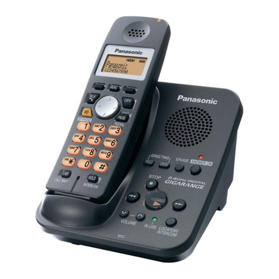
KX-TG3531BXS/KX-TG3531BXB/KX-TG3532BXS/TG3532BXB/KX-TGA351S/KX-TGA351B 5 Location of Controls and Components 5.1. Controls 5.1.2. Handset 5.1.1. Base Unit 5.2. Displays 5.2.1. Handset Display Items... -
Page 33: Installation Instructions
KX-TG3531BXS/KX-TG3531BXB/KX-TG3532BXS/TG3532BXB/KX-TGA351S/KX-TGA351B 6 Installation Instructions 6.1. Setting Up the Base Unit 6.2. Setting Up the Handset 6.1.1. Connecting the AC Adaptor and 6.2.1. Connecting the AC Adaptor Telephone Line Cord 6.3. Battery Installation/ Replacement... -
Page 34: Battery Charge
KX-TG3531BXS/KX-TG3531BXB/KX-TG3532BXS/TG3532BXB/KX-TGA351S/KX-TGA351B 6.4. Battery Charge 6.4.2. Panasonic Battery Performance 6.4.1. Battery Level... -
Page 35: Operation Instructions
KX-TG3531BXS/KX-TG3531BXB/KX-TG3532BXS/TG3532BXB/KX-TGA351S/KX-TGA351B 7 Operation Instructions 7.1. Programmable Settings You can customize the unit by programming the following features using the handset. To access the features, there are 2 methods: - scrolling through the display menus - using the direct commands • Mainly the direct command method is used in these operating instructions. - Page 36 KX-TG3531BXS/KX-TG3531BXB/KX-TG3532BXS/TG3532BXB/KX-TGA351S/KX-TGA351B 7.1.2. Programming using the Direct Commands...
-
Page 37: Copying Handset Phonebook Items
KX-TG3531BXS/KX-TG3531BXB/KX-TG3532BXS/TG3532BXB/KX-TGA351S/KX-TGA351B 7.2. Copying Handset Phonebook Items You can copy one or all of the phonebook items from one handset to another. 7.2.1. Copying all items 7.3. Dial Lock For Service Hint: *: If the current password is forgetten, enter "726276642" and you will be able to go to step 3. -
Page 38: Error Messages
KX-TG3531BXS/KX-TG3531BXB/KX-TG3532BXS/TG3532BXB/KX-TGA351S/KX-TGA351B 7.4. Error Messages... -
Page 39: Troubleshooting
KX-TG3531BXS/KX-TG3531BXB/KX-TG3532BXS/TG3532BXB/KX-TGA351S/KX-TGA351B 7.5. Troubleshooting... - Page 40 KX-TG3531BXS/KX-TG3531BXB/KX-TG3532BXS/TG3532BXB/KX-TGA351S/KX-TGA351B...
-
Page 41: Test Mode
KX-TG3531BXS/KX-TG3531BXB/KX-TG3532BXS/TG3532BXB/KX-TGA351S/KX-TGA351B 8 Test Mode 8.1. Adjustment and Test Mode Flow Chart 8.1.1. Test Burst Mode for Base Unit Note: (*1) Refer to Check Table for RF part (P.63). - Page 42 KX-TG3531BXS/KX-TG3531BXB/KX-TG3532BXS/TG3532BXB/KX-TGA351S/KX-TGA351B 8.1.2. TX-CW Mode for Base Unit Note: (*1) Refer to Check Table for RF part (P.63).
- Page 43 KX-TG3531BXS/KX-TG3531BXB/KX-TG3532BXS/TG3532BXB/KX-TGA351S/KX-TGA351B 8.1.3. RX-CW Test Mode for Base Unit Note: (*1) Refer to Check Table for RF part (P.63).
- Page 44 KX-TG3531BXS/KX-TG3531BXB/KX-TG3532BXS/TG3532BXB/KX-TGA351S/KX-TGA351B 8.1.4. Test Link Mode for Base Unit Note: (*1) Refer to TX-CW Mode for Handset (P.47). If you can not proceed to the next step, refer to Registering a Handset (P.61). (*2) Refer to Check Table for RF part (P.63).
- Page 45 KX-TG3531BXS/KX-TG3531BXB/KX-TG3532BXS/TG3532BXB/KX-TGA351S/KX-TGA351B 8.1.5. Adjustment Mode for Base Unit Cross Reference Check and Adjust Frequency (Base Unit) (P.78) Note: (*1) Refer to the table below, if using Frequency Counter for checking. TEST MODE Frequency (1 Channel) 13.824 MHz → 2400.724512 MHz →...
- Page 46 KX-TG3531BXS/KX-TG3531BXB/KX-TG3532BXS/TG3532BXB/KX-TGA351S/KX-TGA351B 8.1.6. Test Burst Mode for Handset Note: (*1) LCD displays the Channel number. (exception: default/ CH00 = 1ch.) (*2) Refer to Check Table for RF part (P.63).
- Page 47 KX-TG3531BXS/KX-TG3531BXB/KX-TG3532BXS/TG3532BXB/KX-TGA351S/KX-TGA351B 8.1.7. TX-CW Mode for Handset Note: (*1) LCD displays the Channel number. (exception: default/ CH00 = 1ch.) (*2) Refer to Check Table for RF part (P.63).
- Page 48 KX-TG3531BXS/KX-TG3531BXB/KX-TG3532BXS/TG3532BXB/KX-TGA351S/KX-TGA351B 8.1.8. RX-CW Test Mode for Handset Note: (*1) LCD displays the Channel number. (exception: default/ CH00 = 1ch.) (*2) Refer to Check Table for RF part (P.63).
- Page 49 KX-TG3531BXS/KX-TG3531BXB/KX-TG3532BXS/TG3532BXB/KX-TGA351S/KX-TGA351B 8.1.9. Test Link Mode for Handset Note: (*1) LCD displays the Channel number. (exception: default/ CH00 = 1ch.) (*2) If can not proceed to the next step, refer to Registering a Handset (P.61). (*3) for factory use only. (*4) Refer to Check Table for RF part (P.63).
- Page 50 KX-TG3531BXS/KX-TG3531BXB/KX-TG3532BXS/TG3532BXB/KX-TGA351S/KX-TGA351B 8.1.10. Adjustment Mode for Handset Cross Reference (*1) Adjust Battery Low Detector Voltage (Handset) (P.78) Note: (*2) These are the default values. (*3) These values may not be fixed depending on the battery strength. (*4) Refer to the table below, if using Frequency Counter for checking.
-
Page 51: Service Mode
KX-TG3531BXS/KX-TG3531BXB/KX-TG3532BXS/TG3532BXB/KX-TGA351S/KX-TGA351B 9 Service Mode 9.1. How to Clear User Setting Units are reset to the Factory settings by this operation (Erase recorded Voice messages, stored Phone numbers, Caller list and etc.). This operation should not be performed for a usual repair. - Page 52 KX-TG3531BXS/KX-TG3531BXB/KX-TG3532BXS/TG3532BXB/KX-TGA351S/KX-TGA351B 9.1.2. Handset Note: (*1) Be sure to short the battery terminals of the Handset with a lead wire, etc. for 2 seconds for discharge after removing the battery.
-
Page 53: Copying Phonebook Items When Repairing
KX-TG3531BXS/KX-TG3531BXB/KX-TG3532BXS/TG3532BXB/KX-TGA351S/KX-TGA351B 9.2. Copying Phonebook Items when Repairing You can copy the handset phonebook to another (compatible Panasonic) handset. This will help to save the original phonebook data which the customer has registered. Refer to the following procedures. - Page 54 KX-TG3531BXS/KX-TG3531BXB/KX-TG3532BXS/TG3532BXB/KX-TGA351S/KX-TGA351B Note: • If the max number of handsets are already registered to the base unit, a new handset cannot be registered. • To register the handset, refer to Registering a Handset (P.61). • To cancel the handset, refer to Deregistering a Handset (P.61).
-
Page 55: Troubleshooting Guide
KX-TG3531BXS/KX-TG3531BXB/KX-TG3532BXS/TG3532BXB/KX-TGA351S/KX-TGA351B 10 Troubleshooting Guide 10.1. Troubleshooting Flowchart Cross Reference: Note: Check Power (P.56) (*1) When a user claims that the unit disconnects a call right Check Playback (P.58) after the greeting message and no incoming messages can Check Record (P.57) be recorded, this symptom can not be reappeared with TEL Check Battery Charge (P.58) - Page 56 KX-TG3531BXS/KX-TG3531BXB/KX-TG3532BXS/TG3532BXB/KX-TGA351S/KX-TGA351B 10.1.1. Check Power Cross Reference: Note: Power Supply Circuit (P.13) DSP is IC501. Reset Circuit (P.15) (*1) Refer to Specifications (P.5) for part number and sup- ply voltage of AC adaptor. (*2) Refer to Circuit Board (Base Unit_Main) (P.93).
- Page 57 KX-TG3531BXS/KX-TG3531BXB/KX-TG3532BXS/TG3532BXB/KX-TGA351S/KX-TGA351B 10.1.2. Check Record BASE UNIT A) Not record Greeting Message B) Not record Incoming Message C) How to change the Auto Disconnect activation (time) Some Telephone Company lines (fiber or cable) ON Hook and OFF Hook voltages are lower than conventional lines, which may cause a malfunction of Auto Disconnect detection.
- Page 58 KX-TG3531BXS/KX-TG3531BXB/KX-TG3532BXS/TG3532BXB/KX-TGA351S/KX-TGA351B 10.1.3. Check Playback Cross Reference: Note: Power Supply Circuit (P.13) Flash Memory is IC601. DSP is IC501. 10.1.4. Check Battery Charge Note: (*1) Refer to Specifications (P.5) for part number and supply voltage of AC adaptor.
- Page 59 KX-TG3531BXS/KX-TG3531BXB/KX-TG3532BXS/TG3532BXB/KX-TGA351S/KX-TGA351B 10.1.5. Check Link Note: DSP is IC501. (*1) Refer to Check the RF part (P.60). Cross Reference: Check the RF part (P.60)
- Page 60 KX-TG3531BXS/KX-TG3531BXB/KX-TG3532BXS/TG3532BXB/KX-TGA351S/KX-TGA351B 10.1.6. Check the RF part 10.1.6.1. Finding out the Defective part After All the Checkings or Repairing 1. Re-register the checked Handset to the checked Base Unit, and Regular HS to Regular BU. Note: (*1) HS: Handset (*2) BU: Base Unit...
-
Page 61: Registering A Handset
KX-TG3531BXS/KX-TG3531BXB/KX-TG3532BXS/TG3532BXB/KX-TGA351S/KX-TGA351B 10.1.6.1.1. Registering a Handset 10.1.6.1.2. Deregistering a Handset 10.1.6.1.3. Deregistering all handsets by the base unit... - Page 62 KX-TG3531BXS/KX-TG3531BXB/KX-TG3532BXS/TG3532BXB/KX-TGA351S/KX-TGA351B 10.1.6.2. RF Check Flowchart Each item (1 ~ 6) of RF Check Flowchart corresponds to Check Table for RF part (P.63). Please refer to the each item. Note: (*1) Refer to Things to Do after Replacing IC or X'tal (P.78)
- Page 63 KX-TG3531BXS/KX-TG3531BXB/KX-TG3532BXS/TG3532BXB/KX-TGA351S/KX-TGA351B 10.1.6.3. Check Table for RF part Item BU (Base Unit) Check HS (Handset) Check Link Confirmation Normal 1. Register Regular HS to BU (to be 1. Register HS (to be checked) to Regular checked). HS, BU Mode [Normal Mode] 2.
- Page 64 KX-TG3531BXS/KX-TG3531BXB/KX-TG3532BXS/TG3532BXB/KX-TGA351S/KX-TGA351B 10.1.6.4. TEST RANGE Check Circuit block which range is defective can be found by the following check. Item BU (Base Unit) Check HS (HandSet) Check Range Confirmation TX TEST 1. Register Regular HS to BU (to be checked). 1. Register HS (to be checked) to Regular BU.
- Page 65 KX-TG3531BXS/KX-TG3531BXB/KX-TG3532BXS/TG3532BXB/KX-TGA351S/KX-TGA351B 10.1.6.5. RF-DSP Interface Signal Wave Form Test Burst Mode:...
- Page 66 KX-TG3531BXS/KX-TG3531BXB/KX-TG3532BXS/TG3532BXB/KX-TGA351S/KX-TGA351B Test Burst Mode:...
-
Page 67: Check Handset Transmission
KX-TG3531BXS/KX-TG3531BXB/KX-TG3532BXS/TG3532BXB/KX-TGA351S/KX-TGA351B 10.1.7. Check Handset Transmission Cross Reference: Signal Route (P.30) 10.1.8. Check Handset Reception Cross Reference: Signal Route (P.30) Note: When checking the RF part, Refer to Check the RF part (P.60). 10.1.9. Check Caller ID Cross Reference: Telephone Line Interface (P.16) Calling Line Identification (Caller ID) (P.19) -
Page 68: How To Replace The Flat Package Ic
KX-TG3531BXS/KX-TG3531BXB/KX-TG3532BXS/TG3532BXB/KX-TGA351S/KX-TGA351B 10.2. How to Replace the Flat Package IC 10.2.1. Preparation • PbF (: Pb free) Solder • Soldering Iron Tip Temperature of 700°F ± 20°F (370°C ± 10°C) Note: We recommend a 30 to 40 Watt soldering iron. An expert may be able to use a 60 to 80 Watt iron where someone with less experience could overheat and damage the PCB foil. - Page 69 KX-TG3531BXS/KX-TG3531BXB/KX-TG3532BXS/TG3532BXB/KX-TGA351S/KX-TGA351B 10.2.3. How to Install the IC 1. Temporarily fix the FLAT PACKAGE IC, soldering the two marked pins. *Check the accuracy of the IC setting with the corresponding soldering foil. 2. Apply flux to all pins of the FLAT PACKAGE IC.
-
Page 70: How To Replace The Llp (Leadless Leadframe Package) Ic
KX-TG3531BXS/KX-TG3531BXB/KX-TG3532BXS/TG3532BXB/KX-TGA351S/KX-TGA351B 10.3. How to Replace the LLP (Leadless Leadframe Package) IC 10.3.1. Preparation • PbF (: Pb free) Solder • Soldering Iron Tip Temperature of 700°F ± 20°F (370°C ± 10°C) Note: We recommend a 30 to 40 Watt soldering iron. An expert may be able to use a 60 to 80 Watt iron where someone with less experience could overheat and damage the PCB foil. - Page 71 KX-TG3531BXS/KX-TG3531BXB/KX-TG3532BXS/TG3532BXB/KX-TGA351S/KX-TGA351B 10.3.4. How to Install the IC 1. Place the solder a little on the land where the radiation GND pad on IC bottom is to be attached. 2. Place the solder a little on the land where IC pins are to be attached, then place the IC.
-
Page 72: Disassembly And Assembly Instructions
KX-TG3531BXS/KX-TG3531BXB/KX-TG3532BXS/TG3532BXB/KX-TGA351S/KX-TGA351B 11 Disassembly and Assembly Instructions 11.1. Disassembly Instructions 11.1.1. Base Unit... - Page 73 KX-TG3531BXS/KX-TG3531BXB/KX-TG3532BXS/TG3532BXB/KX-TGA351S/KX-TGA351B...
- Page 74 KX-TG3531BXS/KX-TG3531BXB/KX-TG3532BXS/TG3532BXB/KX-TGA351S/KX-TGA351B 11.1.2. Handset...
- Page 75 KX-TG3531BXS/KX-TG3531BXB/KX-TG3532BXS/TG3532BXB/KX-TGA351S/KX-TGA351B 11.1.3. Charger Unit...
-
Page 76: How To Replace The Handset Lcd
KX-TG3531BXS/KX-TG3531BXB/KX-TG3532BXS/TG3532BXB/KX-TGA351S/KX-TGA351B 11.2. How to Replace the Handset LCD... -
Page 77: Antenna Soldering Work
KX-TG3531BXS/KX-TG3531BXB/KX-TG3532BXS/TG3532BXB/KX-TGA351S/KX-TGA351B 11.3. Antenna soldering work Preparation • PbF (: Pb free) Solder • Soldering Iron Tip Temperature of 700°F ± 20°F (370°C ± 10°C) Note: We recommend a 30 to 40 Watt soldering iron. Solder the antenna P.C. board as below. -
Page 78: Measurements And Adjustments
KX-TG3531BXS/KX-TG3531BXB/KX-TG3532BXS/TG3532BXB/KX-TGA351S/KX-TGA351B 12 Measurements and Adjustments 12.1. Things to Do after Replacing IC or X'tal 12.1.1. Preparation Equipment: Frequency counter Check Point for measurement: BCK Checking tolerance: 13.824MHz ± 100Hz (Base Unit)/13.824MHz ± 100Hz (Handset) 12.1.2. Check and Adjust Frequency (Base Unit) 1. -
Page 79: Base Unit Reference Drawing
KX-TG3531BXS/KX-TG3531BXB/KX-TG3532BXS/TG3532BXB/KX-TGA351S/KX-TGA351B 12.2. Base Unit Reference Drawing When connecting the Simulator Equipment for checking, please refer to below. 9.0 V CN101 Spectrum analyzer CN301 JOINT1 ANT1 FL701 C711 L703 L713 L702 D703 L704 L706 C710 C706 C704 C743 L701 C741 TP_TESTN... -
Page 80: Handset Reference Drawing
KX-TG3531BXS/KX-TG3531BXB/KX-TG3532BXS/TG3532BXB/KX-TGA351S/KX-TGA351B 12.3. Handset Reference Drawing When connecting the Simulator Equipment for checking, please refer to below. Note: (*1) is referred to No.3 of Check Table for RF part (P.63). -
Page 81: Frequency Table
KX-TG3531BXS/KX-TG3531BXB/KX-TG3532BXS/TG3532BXB/KX-TGA351S/KX-TGA351B 12.4. Frequency Table Channel TX/RX Frequency TEST MODE Frequency (MHz) (MHz) Channel TX/RX Frequency TEST MODE Frequency 2457.104150 2456.914307 (MHz) (MHz) 2457.994043 2457.804199 2400.914355 2400.724512 2458.887891 2458.698047 2401.808203 2401.618359 2459.777783 2459.587939 2402.698096 2402.508252 2460.671631 2460.481787 2403.591943 2403.402100 2461.561523 2461.371680 2404.481836... -
Page 82: Schematic Diagram
KX-TG3531BXS/KX-TG3531BXB/KX-TG3532BXS/TG3532BXB/KX-TGA351S/KX-TGA351B 13 Schematic Diagram 13.1. For Schematic Diagram 13.1.1. Base Unit (Schematic Diagram (Base Unit_Main)) 13.1.1.1. Acoustic Testing Mode Notes: 1. DC voltage measurements are taken with voltmeter from the negative voltage line. 2. The schematic diagrams may be modified at any time with the development of new technology. - Page 83 KX-TG3531BXS/KX-TG3531BXB/KX-TG3532BXS/TG3532BXB/KX-TGA351S/KX-TGA351B Memo...
-
Page 84: Schematic Diagram (Base Unit_Main)
KX-TG3531BXS/KX-TG3531BXB/KX-TG3532BXS/TG3532BXB/KX-TGA351S/KX-TGA351B 13.2. Schematic Diagram (Base Unit_Main) RF Interface 2.5 V V_PA V_PA V_RF V_RF VOUT PA_CONT PA_CONT PA_CONT IC612 2.5 V SYN_OUT SYN_OUT SYN_OUT 4.0 V SYN_DATA SYN_DATA SYN_DATA SYN_CLK SYN_CLK SYN_CLK SYN_EN VOUT SYN_EN SYN_EN IC301 TX_DATA TX_DATA TX_DATA... - Page 85 KX-TG3531BXS/KX-TG3531BXB/KX-TG3532BXS/TG3532BXB/KX-TGA351S/KX-TGA351B 4.0 V 3.3 V 4.0V CONVERTOR IC331 Q300 L300 22uH VOUT VDET *RESET REFERENCE 1XX : TEL LINE 3XX : POWER, CHARGE 4XX : RESET, MIC, SP IC300 5XX : DSP, RF I/F 6XX : FLASH, KEY, LCD 7XX : RF(2.4G) ON/*OFF 8XX : RF(5.8G)
-
Page 86: Schematic Diagram (Base Unit_Rf Part)
KX-TG3531BXS/KX-TG3531BXB/KX-TG3532BXS/TG3532BXB/KX-TGA351S/KX-TGA351B 13.3. Schematic Diagram (Base Unit_RF Part) PA_CONT 2.5 V (MOD_EN) V_PA L702 V_RF 10nH 2.5 V SYN_OUT SYN_DATA SYN_EN SYN_CLK R719 TX_DATA L705 R730 RX_GAIN 10nH C760 D10P C790 K1000P C737 K470P C783 K1000P C791 C717 2.4 GHz TX... -
Page 87: Schematic Diagram (Base Unit_Operation)
KX-TG3531BXS/KX-TG3531BXB/KX-TG3532BXS/TG3532BXB/KX-TGA351S/KX-TGA351B 13.4. Schematic Diagram (Base Unit_Operation) SPP2 SPN2 2APVCC LED904 MEG_LED LED903 ANS_LED LED902 INUSE_LED KEYS_A KEYS_B KEYS_C KEYS_D KEYIN3 KEYIN2 KEYIN1 DOWN SKIP LOCAT/INT ERASE STOP MSG/VM NC: No Components KX-TG3531/3532 SCHEMATIC DIAGRAM (Base Unit_Operation) -
Page 88: Schematic Diagram (Handset_Main)
KX-TG3531BXS/KX-TG3531BXB/KX-TG3532BXS/TG3532BXB/KX-TGA351S/KX-TGA351B 13.5. Schematic Diagram (Handset_Main) RF circuit BCLK BCLK Flash memory for booting RSSI RSSI TX_DATA TX_DATA PA_CONT PA_CONT RX_EN *RESET RX_EN TX_EN TX_EN IC546 RX_GAIN RX_GAIN DSP Part (control circuit) RX_DATA RX_DATA RF control line R540 C540 K0.1 X501 SHCTRL 13.824MHZ... - Page 89 KX-TG3531BXS/KX-TG3531BXB/KX-TG3532BXS/TG3532BXB/KX-TGA351S/KX-TGA351B TEST SIGNAL FREQUENCY: 1kHz SP phone TX Voice circuit -43 dBm/600 Rear speaker 30 mVp-p C427 D10P L427 NC SP phone RX (MIC Mute: ON) L426 NC 1.8 Vp-p/8 (Vol. Max) Headset TX R431 -37 dBm/600 Headset detection TR...
-
Page 90: Schematic Diagram (Handset_Rf Part)
KX-TG3531BXS/KX-TG3531BXB/KX-TG3532BXS/TG3532BXB/KX-TGA351S/KX-TGA351B 13.6. Schematic Diagram (Handset_RF Part) PA_CONT 3.3 V (MOD_EN) V_PA L702 V_RF 10nH 2.5 V SYN_OUT SYN_DATA SYN_EN SYN_CLK R719 TX_DATA L705 R730 RX_GAIN 10nH C760 D10P C790 K1000P C737 K470P C783 K1000P C717 C791 D10P 2.4 GHz TX... -
Page 91: Schematic Diagram (Charger Unit)
KX-TG3531BXS/KX-TG3531BXB/KX-TG3532BXS/TG3532BXB/KX-TGA351S/KX-TGA351B 13.7. Schematic Diagram (Charger Unit) NC: No Components SCHEMATIC DIAGRAM (Charger Unit) - Page 92 KX-TG3531BXS/KX-TG3531BXB/KX-TG3532BXS/TG3532BXB/KX-TGA351S/KX-TGA351B Memo...
-
Page 93: Printed Circuit Board
KX-TG3531BXS/KX-TG3531BXB/KX-TG3532BXS/TG3532BXB/KX-TGA351S/KX-TGA351B 14 Printed Circuit Board 14.1. Circuit Board (Base Unit_Main) 14.1.1. Component View V_PA V_RF CN101 CN301 JOINT1 ANT1 FL701 C711 L703 L713 L702 D703 L704 L706 C710 C704 C706 C743 L701 TP_TESTN C741 L790 C792 IC701 C744 R706 C760... - Page 94 KX-TG3531BXS/KX-TG3531BXB/KX-TG3532BXS/TG3532BXB/KX-TGA351S/KX-TGA351B 14.1.2. Flow Solder Side View ANT_HOT DCM DCM2 ANT_GND DCP2 D101 IC612 Q141 BCLK Q143 Q142 Q156 Q161 KEY3/TE KEY2 KEY1 KEYB FCLK FRST IC611 MIN2 MIP2 MIC1 PQUP11457Z KX-TG3531/3532 CIRCUIT BOARD (Base Unit_Main (Flow Solder Side View))
-
Page 95: Circuit Board (Base Unit_Rf Part)
KX-TG3531BXS/KX-TG3531BXB/KX-TG3532BXS/TG3532BXB/KX-TGA351S/KX-TGA351B 14.2. Circuit Board (Base Unit_RF Part) FL701 C711 L703 L713 L702 D703 L704 L706 C710 C706 C704 C743 L701 TP_TESTN C741 L790 C792 IC701 C744 R706 C760 C746 C766 C765 C717 C780 KX-TG3531/3532 CIRCUIT BOARD (Base Unit_RF Part (Component View)) -
Page 96: Circuit Board (Base Unit_Antenna)
KX-TG3531BXS/KX-TG3531BXB/KX-TG3532BXS/TG3532BXB/KX-TGA351S/KX-TGA351B 14.3. Circuit Board (Base Unit_Antenna) KX-TG3531/3532 CIRCUIT BOARD (Base Unit_Antenna) -
Page 97: Circuit Board (Base Unit_Operation)
KX-TG3531BXS/KX-TG3531BXB/KX-TG3532BXS/TG3532BXB/KX-TGA351S/KX-TGA351B 14.4. Circuit Board (Base Unit_Operation) 14.4.1. Component View LED903 ERASE BLACK STOP MSG/VM LED904 SKIP DOWN LED902 LOCAT/INT KX-TG3031/32 PQUP11459Z KX-TG3531/3532 CIRCUIT BOARD (Base Unit_Operation (Component View)) - Page 98 KX-TG3531BXS/KX-TG3531BXB/KX-TG3532BXS/TG3532BXB/KX-TGA351S/KX-TGA351B 14.4.2. Flow Solder Side View WBX02 KX-TG3031H PQUP11459Z WBX01 KX-TG3531/3532 CIRCUIT BOARD (Base Unit_Operation (Flow Solder Side View))
-
Page 99: Circuit Board (Handset_Main)
KX-TG3531BXS/KX-TG3531BXB/KX-TG3532BXS/TG3532BXB/KX-TGA351S/KX-TGA351B 14.5. Circuit Board (Handset_Main) 14.5.1. Component View KX-TGA30 R PQUP11462Z L705 R719 C752 C756 C783 RA701 C737 C790 R730 R709 C761 C784 C791 C722 R791 C777 C796 C738 C776 R740 C798 C762 C718 L711 R731 D704 C763 R743 C710... - Page 100 KX-TG3531BXS/KX-TG3531BXB/KX-TG3532BXS/TG3532BXB/KX-TGA351S/KX-TGA351B 14.5.2. Flow Solder Side View LED561 SYN_OUT TAPE LED557 LED559 LED558 LED555 LED556 LEFT MENU RIGHT TALK BACK NEXT PAUSE DOWN HOLD FLASH KX-TGA351 CIRCUIT BOARD (Handset (Flow Solder Side View))
-
Page 101: Circuit Board (Handset_Rf Part)
KX-TG3531BXS/KX-TG3531BXB/KX-TG3532BXS/TG3532BXB/KX-TGA351S/KX-TGA351B 14.6. Circuit Board (Handset_RF Part) L705 R719 C752 C756 C783 RA701 C737 C790 R730 R709 C761 C784 C791 C722 R791 C777 C796 C738 C776 R740 C798 C762 C718 R731 D704 L711 C763 R743 C710 C779 R741 TP_TESTN C764 R742... -
Page 102: Circuit Board (Charger Unit)
KX-TG3531BXS/KX-TG3531BXB/KX-TG3532BXS/TG3532BXB/KX-TGA351S/KX-TGA351B 14.7. Circuit Board (Charger Unit) 14.7.1. Component View PQJT01 PQHG PQHG01 PQHG02 PQHG PQJT02 PQLV30054 PQUP11464Z CIRCUIT BOARD (Charger Unit (Component View)) 14.7.2. Flow Solder Side View PQUP11464Z PQLV30054 CIRCUIT BOARD (Charger Unit (Flow Solder Side View)) -
Page 103: Appendix Information Of Schematic Diagram
KX-TG3531BXS/KX-TG3531BXB/KX-TG3532BXS/TG3532BXB/KX-TGA351S/KX-TGA351B 15 Appendix Information of Schematic Diagram 15.1. CPU Data (Base Unit) 15.1.1. IC501 Description High High_Z 60 KEY_IN6 Key In Description High High_Z 61 KEY_IN5 Key In GNDPA 62 KEY_IN4 Key In SPOUTP 63 KEY_IN3 Key In BCLK 64 KEY_IN2... -
Page 104: Cpu Data (Handset)
KX-TG3531BXS/KX-TG3531BXB/KX-TG3532BXS/TG3532BXB/KX-TGA351S/KX-TGA351B 15.2. CPU Data (Handset) 15.2.1. IC501 Description High High_Z 60 NC Normal Description High High_Z 61 NC Normal GNDPA 62 NC Normal SPOUTP 63 KEYSTROBE _E Active BCLK 64 KEYSTROBE _D Active RSSI 65 KEYSTROBE _C Active 66 KEYSTROBE _B... -
Page 105: Explanation Of Ic Terminals (Rf Part)
KX-TG3531BXS/KX-TG3531BXB/KX-TG3532BXS/TG3532BXB/KX-TGA351S/KX-TGA351B 15.3. Explanation of IC Terminals (RF Part) IC701 15.3.1. -
Page 106: Terminal Guide Of The Ics, Transistors And Diodes
KX-TG3531BXS/KX-TG3531BXB/KX-TG3532BXS/TG3532BXB/KX-TGA351S/KX-TGA351B 15.4. Terminal Guide of the ICs, Transistors and Diodes 15.4.1. Base Unit 15.4.2. Handset... -
Page 107: Exploded View And Replacement Parts List
KX-TG3531BXS/KX-TG3531BXB/KX-TG3532BXS/TG3532BXB/KX-TGA351S/KX-TGA351B 16 Exploded View and Replacement Parts List 16.1. Cabinet and Electrical Parts (Base Unit) -
Page 108: Cabinet And Electrical Parts (Handset)
KX-TG3531BXS/KX-TG3531BXB/KX-TG3532BXS/TG3532BXB/KX-TGA351S/KX-TGA351B 16.2. Cabinet and Electrical Parts (Handset) Note: (*1) This cable is fixed by welding. Refer to How to Replace the Handset LCD (P.76). (*2) Attach the spacer (No. 121) to the exact location described above. -
Page 109: Cabinet And Electrical Parts (Charger Unit)
KX-TG3531BXS/KX-TG3531BXB/KX-TG3532BXS/TG3532BXB/KX-TGA351S/KX-TGA351B 16.3. Cabinet and Electrical Parts (Charger Unit) -
Page 110: Accessories And Packing Materials
KX-TG3531BXS/KX-TG3531BXB/KX-TG3532BXS/TG3532BXB/KX-TGA351S/KX-TGA351B 16.4. Accessories and Packing Materials 16.4.1. KX-TG3531BXS/BXB... - Page 111 KX-TG3531BXS/KX-TG3531BXB/KX-TG3532BXS/TG3532BXB/KX-TGA351S/KX-TGA351B 16.4.2. KX-TG3532BXS/BXB...
- Page 112 KX-TG3531BXS/KX-TG3531BXB/KX-TG3532BXS/TG3532BXB/KX-TGA351S/KX-TGA351B 16.4.3. KX-TGA351BXS/BXB...
-
Page 113: Replacement Parts List
PS-HB TG3531BXB) (for KX-TG3532BXB) available. PQHA10023Z RUBBER PARTS, FOOT CUSHION 2. Important safety notice PQGT19647Z NAME PLATE (for KX-TG3531BXS) Components identified by the mark indicates special (for KX-TG3532BXB) PQGT19718Z NAME PLATE (for KX-TG3531BXB) characteristics important for safety. When replacing any... - Page 114 KX-TG3531BXS/KX-TG3531BXB/KX-TG3532BXS/TG3532BXB/KX-TGA351S/KX-TGA351B Ref. Part No. Part Name & Description Remarks Ref. Part No. Part Name & Description Remarks L711 MQLRF3N9DFB COIL (CAPACITORS) L713 MQLRF18NJFB COIL C101 F1K2J681A006 680P L790 G1C1R0KA0096 COIL C102 F1K2J681A006 680P (JACKS) C111 F1J2A473A024 0.047 CN101 K2LB102B0053 JACK, MODULAR...
- Page 115 KX-TG3531BXS/KX-TG3531BXB/KX-TG3532BXS/TG3532BXB/KX-TGA351S/KX-TGA351B Ref. Part No. Part Name & Description Remarks Ref. Part No. Part Name & Description Remarks C752 ECUE1H2R0CCQ PQKF10729Z3 CABINET COVER (for ABS-HB TGA351BXS) C756 ECUE1H100DCQ PQKF10729Z4 CABINET COVER (for ABS-HB C760 ECUE1H100DCQ TGA351BXB) C762 ECUE1H101JCQ 100P PQGT19650Z NAME PLATE (for KX-TGA351BXS)
- Page 116 KX-TG3531BXS/KX-TG3531BXB/KX-TG3532BXS/TG3532BXB/KX-TGA351S/KX-TGA351B Ref. Part No. Part Name & Description Remarks Ref. Part No. Part Name & Description Remarks CA574 F5A841040004 CAPACITOR ARRAY C501 ECUE1H100DCQ RA401 D1H410220001 RESISTOR ARRAY C502 ECUE1H100DCQ RA402 D1H422220001 RESISTOR ARRAY C503 ECUE0J105KBQ RA403 D1H468020001 RESISTOR ARRAY C504...
-
Page 117: Charger Unit
(*1) You can download and refer to the Operating Instruc- Part No. Part Name & Description Remarks tions (Instruction book) on TSN Server. PQZZ430PIR TIP OF SOLDERING IRON 16.5.4.1. KX-TG3531BXS/BXB PQZZ430PRB RUBBER OF SOLDERING IRON Ref. Part No. Part Name & Description Remarks...