Sony MZ-RH910 Service Manual
Hide thumbs
Also See for MZ-RH910:
- Manual de instrucciones (119 pages) ,
- Operating instructions manual (115 pages) ,
- Specifications (2 pages)
Table of Contents
Advertisement
Quick Links
Download this manual
See also:
Operating Instructions
SERVICE MANUAL
Ver. 1.0 2005.03
US and foreign patents licensed from Dolby Laboratories.
• SonicStage is trademark or registered trademark of Sony Corporation.
• MD Simple Burner, OpenMG, "MagicGate", "MagicGate Memory
Stick", "Memory Stick", Hi-MD, Net MD, ATRAC, ATRAC3,
ATRAC3plus and their logos are trademarks of Sony Corporation.
• Microsoft, Windows, Windows NT and Windows Media are trademarks
or registered trademarks of Microsoft Corporation in the United States
and /or other countries.
• IBM and PC/AT are registered trademarks of International Business
Machines Corporation.
• Macintosh is a trademark of Apple Computer, Inc. in the United States
and/ or other countries.
• Pentium is a trademark or registered trademark of Intel Corporation.
• All other trademarks and registered trademarks are trademarks or
registered trademarks of their respective holders.
• ™ and ® marks are omitted in this manual.
• CD and music-related data from Gracenote, Inc., copyright © 2000-
2004 Gracenote. Gracenote CDDB ® Client Software, copyright 2000-
2004 Gracenote. This product and service may practice one or more of
the following U.S. Patents: #5,987,525; #6,061,680; #6,154,773,
#6,161,132, #6,230,192, #6,230,207, #6,240,459, #6,330,593, and other
patents issued or pending. Services supplied and/or device manufactured
under license for following Open Globe, Inc. United States Patent
6,304,523.
Gracenote is a registered trademarks of Gracenote. The Gracenote logo
and logotype, and the "Powered by Gracenote" logo are trademarks of
Gracenote.
Program © 2001, 2002, 2003, 2004, 2005 Sony Corporation
Documentation © 2005 Sony Corporation
Sony Corporation
9-879-561-01
Personal Audio Group
2005C05-1
Published by Sony Engineering Corporation
© 2005.03
For other Service and User Manuals, go to www.ManualDepot.com
MZ-RH910
Model Name Using Similar Mechanism
MD Mechanism Type
Optical Pick-up Name
SPECIFICATIONS
Audio playing system
MiniDisc digital audio system
Laser diode properties
Material: GaAlAs
Wavelength: λ = 790 nm
Emission duration: continuous
Laser output: less than 44.6 µW
(This output is the value measured at a distance
of 200 mm from the lens surface on the optical
pick-up block with 7 mm aperture.)
PORTABLE MD RECORDER
US Model
Canadian Model
AEP Model
UK Model
E Model
Australian Model
Tourist Model
NEW
MT-MZNH900-181J
ABX-UJ
– Continued on next page –
Advertisement
Table of Contents

Related Manuals for Sony MZ-RH910


Summary of Contents for Sony MZ-RH910
- Page 1 US and foreign patents licensed from Dolby Laboratories. Model Name Using Similar Mechanism MD Mechanism Type MT-MZNH900-181J • SonicStage is trademark or registered trademark of Sony Corporation. • MD Simple Burner, OpenMG, “MagicGate”, “MagicGate Memory Optical Pick-up Name ABX-UJ Stick”, “Memory Stick”, Hi-MD, Net MD, ATRAC, ATRAC3, ATRAC3plus and their logos are trademarks of Sony Corporation.
- Page 2 When using a 100% fully charged nickel metal hydride rechargeable battery 30 minutes 30 minutes When using a Sony LR6 (size AA) alkaline dry battery (produced in Japan) Approximate time When playing continuously in Hi-MD mode When transferring 4-minute tracks (Unit: approx.hours)(JEITA)
-
Page 3: Table Of Contents
LES DIAGRAMMES SCHÉMATIQUES ET LA LISTE DES PIÈCES SONT CRITIQUES POUR LA SÉCURITÉ DE FONCTIONNEMENT. NE REMPLACER CES COM- POSANTS QUE PAR DES PIÈCES SONY DONT LES NUMÉROS SONT DONNÉS DANS CE MANUEL OU DANS LES SUPPLÉMENTS PUBLIÉS PAR SONY. -
Page 4: Servicing Notes
MZ-RH910 SECTION 1 SERVICING NOTES OPERATION CHECK WHEN THE MAIN BOARD IS NOTES ON HANDLING THE OPTICAL PICK-UP REMOVED BLOCK OR BASE UNIT In making an operation check with the MAIN board removed from The laser diode in the optical pick-up block may suffer electrostatic... -
Page 5: General
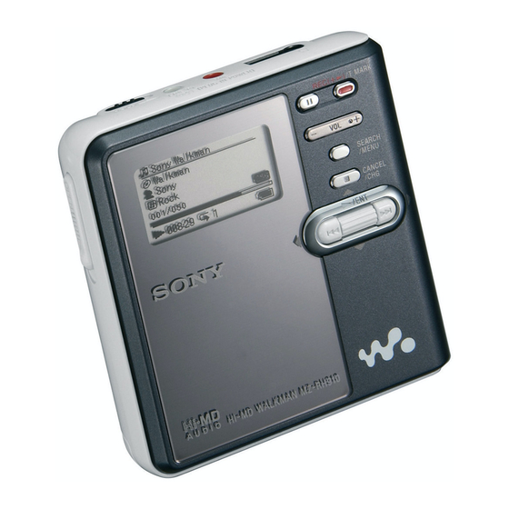
MZ-RH910 SECTION 2 This section is extracted from instruction manual. GENERAL Looking at controls The recorder The display window of the recorder A Operating condition indication display E Hi-MD/MD indication area “Hi-MD” lights up when the disc used Displays the indications of each... -
Page 6: Disassembly
MZ-RH910 SECTION 3 DISASSEMBLY • This set can be disassembled in the order shown below. 3-1. DISASSEMBLY FLOW Note 1: The process described in can be performed in any order. Note 2: Without completing the process described in , the next process can not be performed. -
Page 7: Main Board
MZ-RH910 3-3. MAIN BOARD 3 flexible board (CN471) 1 Remove two solders. 7 MAIN board 2 flexible board (CN701) 6 flexible board (CN501) 1 Remove two solders. 4 five toothed lock screws 3-4. PANEL (UPPER) SECTION 6 panel (upper) section... -
Page 8: Mechanism Deck (Mt-Mznh900-181J)
MZ-RH910 3-5. MECHANISM DECK (MT-MZNH900-181J) 1 two step screws (MD) 2 mechanism (MT-MZNH900-181J) 3-6. BATTERY CASE BLOCK 2 MD standard pin 3 two screws 1 claw 7 battery case block 5 tension spring (lock) 4 screw (M1.4) 6 open slider... -
Page 9: Gear (Bsa), Gear (Sb)
MZ-RH910 3-7. GEAR (BSA), GEAR (SB) 1 self tap screw 2 thrust retainer spring 3 washer (0.8-2.5) 4 gear (BSA) 5 gear (SB) 3-8. OP SERVICE ASSY 1 Lead screw block assy is turned and it removes from OP service assy. -
Page 10: Dc Motor Ssm18D/C-Np (Spindle) (M701), Dc Motor (Sled) (M702), Dc Motor Unit (Over Write Head Up/Down) (M703)
MZ-RH910 3-9. DC MOTOR SSM18D/C-NP (SPINDLE) (M701), DC MOTOR (SLED) (M702), DC MOTOR UNIT (OVER WRITE HEAD UP/DOWN) (M703) 3 two screws (M1.4) 4 DC motor (sled) (M702) 2 Remove two solders of flexible board. 1 Remove four solders of flexible board. -
Page 11: Position Of Ferrite Core
MZ-RH910 3-11. POSITION OF FERRITE CORE -AC ADAPTOR- A cable is rolled twice. clamp filter (ferrite core) (Part No. 1-400-878-11) -USB CABLE- A cable is rolled once. USB A type USB mini B type clamp filter (ferrite core) (Part No. 1-400-878-11) -
Page 12: Test Mode
MZ-RH910 SECTION 4 TEST MODE OUTLINE Remote commander LCD display Operation in the test mode is performed with the set. A key having no particular description in the text, indicates a set key. Also, For the LCD display, the LCD on the remote commander is shown. - Page 13 MZ-RH910 3. MANUAL MODE 5. The display changes a shown below each time the This is mode to adjust or check the operation of the set by function. [SEARCH/MENU] key is pressed. Operation of The Manual Mode • Item Title Display 1.
- Page 14 MZ-RH910 4. OVERALL ADJUSTMENT MODE 4-2. Error Message in The Overall Adjustment Mode 4-1. Operation of The Overall Adjustment Mode In the Overall Adjustment mode, if an error occurred, it displays as 1. Enter the test mode (Display Check mode).
- Page 15 MZ-RH910 Flow of Self-diagnosis Result Display mode operation: 6. KEY CHECK MODE This mode is used for key check. The first error Operation of The Key Check Mode *** 1 #### 1. Enter the test mode (Display Check mode). [VOL +] key [VOL --] key 2.
-
Page 16: Electrical Adjustments
MZ-RH910 SECTION 5 ELECTRICAL ADJUSTMENTS 1. PRECAUTIONS FOR ADJUSTMENT 4. Press the key once, press the [VOL+] key once, and press > 1. Adjustment must be done in the test mode only. After adjusting, key once again to display as follows. - Page 17 MZ-RH910 3-2-3. VBsAdj adjustments ItemNo. Display Specification value Measuring point Procedure: 1.13 V ± 0.01 V 2241 241 REG4 ** CL8001 1. In the “3-2-2. PwrAdj Adjustments” completed status, display 2242 242 REG5 ** 2.05 V + 0.02 V CL8029 as follows.
- Page 18 MZ-RH910 3-3. Charge Function Check 3-4. Laser Power Check Note1: When perform this check, don’t apply a voltage to battery terminals. Procedure: Note2: Be sure to disconnect the AC adapter when connecting the resistors. 1. Enter the test mode (Display Check mode).
- Page 19 MZ-RH910 Example of Calculation: 3-5-3. Other setting Procedure: Result Item No. Parameter 1. Enter the test mode (Display Check mode). Decimal Hexadecimal 2. Press the [VOL+] key to enter the Manual mode. 0211 Pr_nominal 2.48 mW 3. Press the [VOL+] key once and press the key five time to >...
- Page 20 MZ-RH910 3-6. Servo Overall Adjustment Note1: Be sure to adjustment so that the set is horizontal and the LCD is upside. Unless performed in that state, it is not adjusted correctly. Note2: If NG is displayed in the middle of this adjustments, perform “3-2.
-
Page 21: Diagrams
MZ-RH910 SECTION 6 DIAGRAMS 6-1. BLOCK DIAGRAM – MD SERVO Section – OVER WRITE HEAD DRIVE IC601 (1/2) HR601 (Page 23) OVER WRITE OVER 69 HBB HEAD DRIVE WRITE 78 HA Q601, 602 HEAD 70 HAB EFM_CLK LATCH M703 OUTA... -
Page 22: Block Diagram - Audio Section
MZ-RH910 6-2. BLOCK DIAGRAM – AUDIO Section – MUTEON (Page 23) SWITCHING DRIVER, HEADPHONE AMP IC351 DCLSOUTL OUT2 • SIGNAL PATH J351 MUTING FROM IC801 (1/3) Q351 (MD SERVO SECTION) : PLAYBACK DCLSOUTR OUT1 J301 : OPTICAL IN LINE IN... -
Page 23: Block Diagram - Power Supply Section
MZ-RH910 6-3. BLOCK DIAGRAM – POWER SUPPLY Section – (Page 22) SDO0 SCK0 SDO0 (Page 21) DATA CLK 63 SCK0 XWK1, XWK2, XRST XWK4 XWK4 (Page 22) XWK4 SLEEP (Page 22) XWK2 XWK2 4 STRB XRST2 XRST2 XWK1 WAKE UP SWITCH... - Page 24 MZ-RH910 • Note For Printed Wiring Boards and Schematic Diagrams • Waveforms – MAIN Board – Note on Printed Wiring Board: Note on Schematic Diagram: IC501 8 (RFO) IC301 9 (MCLK) • X : parts extracted from the component side.
-
Page 25: Schematic Diagram - Main Board (1/9)
MZ-RH910 • See page 36 for IC Block Diagrams. 6-4. SCHEMATIC DIAGRAM – MAIN Board (1/9) – (1/9) XRST_MTR_DRV XRST_MTR_DRV SLD_CON_W C714 C716 SLD_CON_W SLD_CON_V SLD_CON_V SLD_CON_U SLD_CON_U SLD_PWM SLD_PWM SLD_MON_U SLD_MON_U SLD_MON_V SLD_MON_V SLD_MON_W SLD_MON_W SLD_CON_W SLD_CON_V R707 2.2k R708 2.2k... -
Page 26: Schematic Diagram - Main Board (2/9)
MZ-RH910 • See page 36 for IC Block Diagrams. 6-5. SCHEMATIC DIAGRAM – MAIN Board (2/9) – (2/9) XCS_REC_DRV SUSPEND C673 SUSPEND REG_DACVREFH USB_HOLD USB_HOLD RECP RECP C668 EFM_CLK EFM_CLK C669 C643 VOLTAGE DETECT XCS_REC_DRV IC606 +1.2V REGULATOR XCS_REC_DRV XC61CN1702NR... -
Page 27: Schematic Diagram - Main Board (3/9)
MZ-RH910 • See page 24 for Waveforms. • See page 36 for IC Block Diagrams. 6-6. SCHEMATIC DIAGRAM – MAIN Board (3/9) – (Page 25) (3/9) C553 C554 6.3V C523 C524 C530 (Page 26) 0.01 R505 L503 10µH C519 XLDON... -
Page 28: Schematic Diagram - Main Board (4/9)
MZ-RH910 • See page 36 for IC Block Diagrams. 6-7. SCHEMATIC DIAGRAM – MAIN Board (4/9) – (4/9) (Page 32) Q451 RTQ035P02TR (Page 26) GND_SW C453 VBUS_MON 0.047 BATT_MINUS_MON BATT_MINUS_MON Q451,452 CHG_TYPE2 (BATTERY CASE) CHG_TYPE2 VOLTAGE LIMITER W401 CHG_I_CTL3 CHG_I_CTL3... -
Page 29: Schematic Diagram - Main Board (5/9)
MZ-RH910 • See page 36 for IC Block Diagrams. 6-8. SCHEMATIC DIAGRAM – MAIN Board (5/9) – (Page 26) (5/9) (Page 27) L903 10µH C915 C9001 6.3V 0.01 C922 C923 C958 R968 R969 470k 2.2k 6.3V 6.3V D906 NSR0320MW2T1G Q906... -
Page 30: Schematic Diagram - Main Board (6/9)
MZ-RH910 • See page 24 for Waveforms. • See page 36 for IC Block Diagrams. 6-9. SCHEMATIC DIAGRAM – MAIN Board (6/9) – (Page 26) (6/9) (Page 28) D_VCONT_PWM D_VCONT_PWM R361 DCLSOUTR DCLSOUTR DCLSOUTL DCLSOUTL FS512 Q904 FS512 RTL035N03 XMUTE... -
Page 31: Schematic Diagram - Main Board (7/9)
MZ-RH910 • See page 36 for IC Block Diagrams. 6-10. SCHEMATIC DIAGRAM – MAIN Board (7/9) – (7/9) R478 4.7k R476 R477 4.7k 4.7k (Page 32) CN471 VC01 JOG_B JOG_B JOG_A XRST2 JOG_A SET_KEY_2 R487 SET_KEY_2 SET_KEY_1 SET_KEY_1 REC_KEY R490... -
Page 32: Schematic Diagram - Main Board (8/9)
MZ-RH910 • See page 24 for Waveforms. • See page 41 for IC Pin Function Description. 6-11. SCHEMATIC DIAGRAM – MAIN Board (8/9) – (8/9) OPEN_CLOSE_SW WK_DET (Page 31) R868 SDO0 SDO0 SCK0 R827 SCK0 Q803 OPT_DET 2SC5383-TP-1F R880 R842... -
Page 33: Schematic Diagram - Main Board (9/9)
MZ-RH910 • See page 24 for Waveforms. • See page 36 for IC Block Diagrams. 6-12. SCHEMATIC DIAGRAM – MAIN Board (9/9) – (9/9) +2.1V REGULATOR IC302 Q301 XC6219B212MR 2SA2018TL C327 R304 B+ SWITCH 100k R301 C303 C320 XOPT_CTL R314... -
Page 34: Main Board (Component Side)
MZ-RH910 6-13. PRINTED WIRING BOARD – MAIN Board (Component Side) – : Uses unleaded solder. • Semiconductor Location Ref. No. Location D450 D458 S890 S890 D604 (PROTECT DETECT) D801 D881 D882 S891 S891 D883 HI-MD D884 PROTECT DETECT D885 D904... -
Page 35: Main Board (Conductor Side)
MZ-RH910 6-14. PRINTED WIRING BOARD – MAIN Board (Conductor Side) – : Uses unleaded solder. • Semiconductor Location Ref. No. Location MAIN BOARD (CONDUCTOR SIDE) NICKEL METAL HYBRID D401 J-10 RECHARGEABLE BATTERY D440 F-11 NH-10WM S892 1PC. 1.2V 900mAh D443... - Page 36 MZ-RH910 • IC Block Diagrams IC301 AK5356VN-L IC351 NJU8716AV (TE2) VREGO 1 CFB 2 VG 3 VREF 4 16 VREG MICR 22 VSS 5 RESET LOW VOLTAGE LOW VOLTAGE REGULATOR DETECTOR VDD DETECTOR VRGO MVDD 23 CONTROL MVSS 24 MCK 6...
- Page 37 MZ-RH910 IC501 SN761059AZQLR 42 41 35 34 33 32 31 30 29 SERIAL INTERFACE POWER CPGND VCC2 SUPPLY TEMP A+B+C+D VREF09 NPPO MALFA AVCC2 VCC2 AW+DW AWBPF S-MONITOR TON PEAK OFTRK OFTRK TON BOTM DWBPF ADIP OFTTH T-ON TON-C TWPP...
- Page 38 MZ-RH910 IC601 SC901585VAR2 CHARGE PUMP NC A12 56 LATCH EFM BOTTOM LVDT WAKE 55 XWKO PRE DRIVER HOLD OUT CONTROL HOLD VBUS 54 VBUS LOGIC EFM TOP RST OUT BUFFER PRE DRIVER 53 WAKEC PVBUS PVBUS VBUS 52 V33UO CRST...
- Page 39 MZ-RH910 IC701 SC901583EPR2 56 55 54 53 52 BIAS VC LOW 3PHASE 3PHASE VOLTAGE VI1 1 CONTROL CONTROL DETECTOR WI1 2 GNDW1 3 GNDW2 3PHASE 3PHASE WO1 4 PRE DRIVER PRE DRIVER VMVW1 5 VMVW2 VO1 6 GNDUV1 7 GNDUV2...
- Page 40 MZ-RH910 IC891 AK6512CM-E2 8 VCC CS 1 7 HOLD STATUS REGISTER VREF GENERATOR INSTRUCTION SO 2 DECODE SWITCH CONTROL & CLOCK GENERATION WP 3 DECODER BUFFERS GND 4 EEPROM 64K bit R/W AMPS 8192 × 8 INSTRUCTION & REGISTER AUTO ERASE...
- Page 41 MZ-RH910 • IC Pin Function Description IC801 CXD2681-225GG (SYSTEM CONTROLLER, DSP) Pin No. Pin Name Description DVDD1_0 Power supply terminal (DSP logic system) DVSS1_0 Ground terminal (DSP logic system) DVDD1_1 Power supply terminal (DSP logic system) DVSS1_1 Ground terminal (DSP logic system)
- Page 42 MZ-RH910 Pin No. Pin Name Description DAVDD Power supply terminal (for D/A converter) DVDD25LPF Power supply terminal (for D/A converter) DAVSS Ground terminal (for D/A converter) OSCVDD Power supply terminal (for 22.5792 MHz OSC) USBOSCVDD Power supply terminal (for the USB 48 MHz OSC)
- Page 43 MZ-RH910 Pin No. Pin Name Description FILI Filter input terminal for the playback EFM system master PLL FILO Filter output terminal for the playback EFM system master PLL CLTV Internal VCO control voltage input terminal for the playback EFM system master PLL...
- Page 44 MZ-RH910 Pin No. Pin Name Description VREFR Reference voltage input terminal (for internal D/A converter R-CH) Not used DCLSOUTR PWM modulator signal output to the headphone amplifier (R-CH) DCLSOUTL PWM modulator signal output to the headphone amplifier (L-CH) RTCK Not used ADFG ADIP duplex FM signal (21.05kHz to 23.05 kHz) input from the RF amplifier...
- Page 45 MZ-RH910 Pin No. Pin Name Description BEEP Beep sound control signal output to the headphone amplifier Not used XOPT_CTL Power supply on/off control signal output terminal for the optical input jack Not used EL_PWR_CTL EL power supply on/off control signal output terminal Not used...
- Page 46 MZ-RH910 Pin No. Pin Name Description CS_RTC Chip select signal output to the real time clock Not used JOG_A Jog dial pulse input terminal (A phase) JOG_B Jog dial pulse input terminal (B phase) VBUS_DET Detection terminal of USB power supply...
- Page 47 MZ-RH910 Pin No. Pin Name Description XBCK Bit clock (2.8224 MHz) output to the external A/D converter OSCI Main system clock input terminal (22.5792 MHz) OSCO Main system clock output terminal (22.5792 MHz) FS512 Clock signal (512Fs=22.5792 MHz) output to the headphone amplifier...
-
Page 48: Exploded Views
MZ-RH910 SECTION 7 EXPLODED VIEWS NOTE: • Items marked “*” are not stocked since they • -XX and -X mean standardized parts, so they The components identified by mark 0 or dotted line with mark 0 are may have some difference from the original are seldom required for routine service. -
Page 49: Panel (Upper) Section
MZ-RH910 7-2. PANEL (UPPER) SECTION LCD101 Ref. No. Part No. Description Remark Ref. No. Part No. Description Remark X-2055-986-1 UPPER PANEL ASSY, SVX (BLACK) 2-630-518-01 SHEET (LCD) (EXCEPT US, CND, MX) X-2055-987-1 PANEL (UPER) (S) SV ASSY (SILVER) 2-630-517-01 CUSHION (BUTTON) -
Page 50: Chassis Section
MZ-RH910 7-3. CHASSIS SECTION mechanism deck section (MT-MZNH900-181J) MAIN board Ref. No. Part No. Description Remark Ref. No. Part No. Description Remark 2-595-769-01 SPRING (LOCK), TENSION 2-594-514-01 SPACER (IC) 3-245-889-01 SPRING (LIMITTER), COMPRESSION 2-588-273-01 TERMINAL (SUM3) 3-266-499-01 SLIDER, OPEN 3-238-876-04 SCREW (M1.4), TOOTHED LOCK... -
Page 51: Mechanism Deck Section (Mt-Mznh900-181J)
MZ-RH910 7-4. MECHANISM DECK SECTION (MT-MZNH900-181J) not supplied HR601 (over write head) M702 M703 (including HR601 (over write head) ) M701 The components identified by Les composants identifiés par une mark 0 or dotted line with marque 0 sont critiques pour la mark 0 are critical for safety. -
Page 52: Electrical Parts List
MZ-RH910 SECTION 8 MAIN ELECTRICAL PARTS LIST NOTE: • Items marked “*” are not stocked since they • Due to standardization, replacements in the The components identified by mark 0 or dotted line with mark 0 are parts list may be different from the parts are seldom required for routine service. - Page 53 MZ-RH910 MAIN Ref. No. Part No. Description Remark Ref. No. Part No. Description Remark C518 1-135-210-11 TANTALUM CHIP 4.7uF C635 1-100-539-11 TANTALUM CHIP 47uF 6.3V C519 1-125-777-11 CERAMIC CHIP 0.1uF C520 1-125-777-11 CERAMIC CHIP 0.1uF C636 1-125-777-11 CERAMIC CHIP 0.1uF...
- Page 54 MZ-RH910 MAIN Ref. No. Part No. Description Remark Ref. No. Part No. Description Remark C822 1-125-777-11 CERAMIC CHIP 0.1uF C3304 1-164-943-11 CERAMIC CHIP 0.01uF C823 1-125-777-11 CERAMIC CHIP 0.1uF C827 1-125-777-11 CERAMIC CHIP 0.1uF C3305 1-164-943-11 CERAMIC CHIP 0.01uF C828 1-164-937-11 CERAMIC CHIP 0.001uF...
- Page 55 MZ-RH910 MAIN Ref. No. Part No. Description Remark Ref. No. Part No. Description Remark D605 6-501-201-01 DIODE BAT54XV2T1 IC351 6-706-746-01 IC NJU8716AV (TE2) D606 6-500-909-01 DIODE MA22D1700LS0 @ IC401 6-707-717-01 IC MM1690NCBE D607 6-500-909-01 DIODE MA22D1700LS0 IC471 6-705-715-01 IC XC6219B242MR...
- Page 56 MZ-RH910 MAIN Ref. No. Part No. Description Remark Ref. No. Part No. Description Remark < TRANSISTOR > R255 1-218-929-11 RES-CHIP 1/16W R256 1-218-937-11 RES-CHIP 1/16W Q151 6-550-379-01 FET 2SK354700LS0 R301 1-218-953-11 RES-CHIP 1/16W Q251 6-550-379-01 FET 2SK354700LS0 Q301 8-729-051-23 TRANSISTOR...
- Page 57 MZ-RH910 MAIN Ref. No. Part No. Description Remark Ref. No. Part No. Description Remark R683 1-218-989-11 RES-CHIP 1/16W R477 1-208-699-11 METAL CHIP 4.7K 0.5% 1/16W R684 1-218-965-11 RES-CHIP 1/16W R478 1-218-961-11 RES-CHIP 4.7K 1/16W R685 1-218-965-11 RES-CHIP 1/16W R480 1-218-977-11 RES-CHIP...
- Page 58 MZ-RH910 MAIN SWITCH Ref. No. Part No. Description Remark Ref. No. Part No. Description Remark R6695 1-218-990-11 SHORT CHIP R882 1-218-985-11 RES-CHIP 470K 1/16W R8813 1-218-990-11 SHORT CHIP R883 1-218-989-11 RES-CHIP 1/16W R8891 1-218-953-11 RES-CHIP 1/16W R884 1-218-985-11 RES-CHIP 470K...
- Page 59 MZ-RH910 Ref. No. Part No. Description Remark Ref. No. Part No. Description Remark 2-588-603-61 MANUAL, INSTRUCTION (SWEDISH) (AEP) 2-588-603-71 MANUAL, INSTRUCTION (ITALIAN) (AEP) 2-588-603-81 MANUAL, INSTRUCTION (PORTUGUESE) (AEP, JE) 2-588-603-91 MANUAL, INSTRUCTION (FINNISH) (AEP) 2-588-604-11 MANUAL, INSTRUCTION (CZECH) (EE) 2-588-604-21 MANUAL, INSTRUCTION (HUNGARIAN) (EE)
- Page 60 MZ-RH910 REVISION HISTORY Clicking the version allows you to jump to the revised page. Also, clicking the version at the upper right on the revised page allows you to jump to the next revised page. Ver. Date Description of Revision...