Table of Contents
Advertisement
HCD-TZ100/TZ200/TZ300
SERVICE MANUAL
Ver. 1.1 2009.08
• HCD-TZ100/TZ200/TZ300 are the amplifi er, DVD/CD
and tuner section in DAV-TZ100/TZ200/TZ300.
This system incorporates with Dolby* Digital and Dolby Pro Logic (II)
adaptive matrix surround decoder and the DTS** Digital Surround System.
* Manufactured under license from Dolby Laboratories.
Dolby, Pro Logic, and the double-D symbol are trademarks of Dolby
Laboratories.
** Manufactured under license under U.S. Patent #'s:
5,451,942; 5,956,674; 5,974,380; 5,978,762; 6,487,535 & other U.S.
and worldwide patents issued & pending. DTS and DTS Digital
Surround are registered trademarks and the DTS logos and Symbol are
trademarks of DTS, Inc. © 1996-2008 DTS, Inc. All Rights Reserved.
Amplifi er Section
Stereo mode (rated)
65 W + 65 W (at 3 ohms,
1 kHz, 1% THD)
Surround mode (reference) RMS output power
FL/FR/C/SL/SR*: 83
watts (per channel at 3
ohms, 1 kHz, 10% THD)
Subwoofer*: 85 watts (at 3
ohms, 80 Hz, 10% THD)
* Depending on the decoding mode settings and the
source, there may be no sound output.
Inputs (Analog)
TV/VIDEO (AUDIO IN) Sensitivity: 450/250 mV
Super Audio CD/DVD System
Laser Diode Properties
Emission Duration:
Continuous
Laser Output: Less than
44.6μW
* This output is the value measurement at a distance
of 200mm from the objective lens surface on the
Optical Pick-up Block with 7mm aperture.
Signal format system
Mexican and Latin American models:
NTSC
Other models:
NTSC/PAL
Sony Corporation
9-889-531-02
2009H04-1
Audio&Video Business Group
©
2009.08
Published by Sony Techno Create Corporation
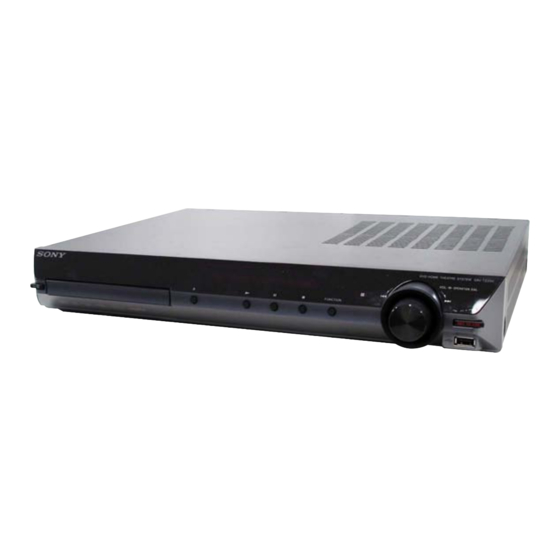
Photo: HCD-TZ200
Model Name Using Similar Mechanism
Mechanism Type
Optical Pick-up Name
SPECIFICATIONS
USB Section
(USB) port:
Maximum current:
500 mA
Tuner Section
System
PLL quartz-locked digital
synthesizer
FM Tuner section
Tuning range
North American models: 87.5 MHz - 108.0 MHz
(100 kHz step)
Other models:
87.5 MHz - 108.0 MHz
(50 kHz step)
Antenna (aerial)
FM wire antenna (aerial)
Antenna (aerial) terminals 75 ohms, unbalanced
Intermediate frequency
10.7 MHz
Video Section
Outputs
VIDEO: 1 Vp-p 75 ohms
HDMI OUT: Type A (19
pin)
General
Power requirements
North American and Mexican models:
120 V AC, 60 Hz
Argentine models:
220 V - 240 V AC,
50/60 Hz
E Model
Australian Model
HCD-TZ200
Mexican Model
HCD-TZ100/TZ200/TZ300
HCD-DZ290K/DZ590K
CDM85-DVBU102
KHM-313CAA
Latin American models:
110 V - 240 V AC,
50/60 Hz
Other models:
220 V - 240 V AC,
50/60 Hz
Power consumption
On: 100 W
Standby: 0.3 W (at the
Power Saving mode)
430 mm × 67 mm × 335
Dimensions (approx.)
mm (w/h/d) incl.
projecting parts
Mass (approx.)
3.5 kg
Supported fi le format
MP3 (MPEG 1 Audio Layer-3)
File Extension:
mp3
Bitrate:
32 kbps - 320 kbps
Sampling frequencies:
32/44.1/48 kHz
WMA (USB device only)
File Extension:
wma
Bitrate:
48 kbps - 192 kbps
Sampling frequencies:
44.1 kHz
– Continued on next page –
DVD RECEIVER
Advertisement
Table of Contents

Related Manuals for Sony HCD-TZ100


Summary of Contents for Sony HCD-TZ100
- Page 1 HCD-TZ200 Mexican Model HCD-TZ100/TZ200/TZ300 Ver. 1.1 2009.08 Photo: HCD-TZ200 • HCD-TZ100/TZ200/TZ300 are the amplifi er, DVD/CD and tuner section in DAV-TZ100/TZ200/TZ300. This system incorporates with Dolby* Digital and Dolby Pro Logic (II) Model Name Using Similar Mechanism HCD-DZ290K/DZ590K adaptive matrix surround decoder and the DTS** Digital Surround System.
- Page 2 THE PARTS LIST ARE CRITICAL TO SAFE OPERATION. mation. REPLACE THESE COMPONENTS WITH SONY PARTS Strictly follow the instructions whenever the components are re- WHOSE PART NUMBERS APPEAR AS SHOWN IN THIS paired and/or replaced. MANUAL OR IN SUPPLEMENTS PUBLISHED BY SONY.
-
Page 3: Table Of Contents
HCD-TZ100/TZ200/TZ300 TABLE OF CONTENTS SERVICING NOTES 5-4. Block Diagram –POWER Section– ........ 24 ..........5-5. Printed Wiring Board –MAIN Section (1/2)– ....26 5-6. Printed Wiring Boards –MAIN Section (2/2)– ....27 DISASSEMBLY 5-7. Schematic Diagram –MAIN Section (1/8)– ....28 2-1. -
Page 4: Servicing Notes
HCD-TZ100/TZ200/TZ300 SECTION 1 SERVICING NOTES How to open the disc table when power switch turns off NOTES ON HANDLING THE OPTICAL PICK-UP Insert a tapering driver into the aperture of the unit bottom, and BLOCK OR BASE UNIT slide it in the direction of the arrow. - Page 5 HCD-TZ100/TZ200/TZ300 Discharge the charged electricity in capacitors to prevent electric shock as follows When disassembling the machine, be sure to discharge the charged electricity in the following capacitors. Use a resistor of 800 ohms, 2 Watts for discharging the following capacitors.
-
Page 6: Disassembly
HCD-TZ100/TZ200/TZ300 SECTION 2 DISASSEMBLY • This set can be disassembled in the order shown below. 2-1. CASE (Page 7) 2-2. LOADING PANEL (Page 7) 2-3. DVD MECHANISM DECK (Page 8) 2-4. FRONT PANEL SECTION 2-9. TRAY (Page 8) (Page 11) 2-5. -
Page 7: Case
HCD-TZ100/TZ200/TZ300 Note: Follow the disassembly procedure in the numerical order given. 2-1. CASE 4 case 2 screw (case 3 TP2) 3 five screws (+BV3 (3-CR)) 1 screw (case 3 TP2) 2-2. LOADING PANEL 3 loading panel tray... -
Page 8: Dvd Mechanism Deck
HCD-TZ100/TZ200/TZ300 2-3. DVD MECHANISM DECK 6 DVD mechanism deck 4 two screws (+BV3 (3-CR)) 5 screw (+BV3 (3-CR)) 2 CN1201 (6P) 1 wire (flat type) (24 core) (CN1101) 3 wire (flat type) (5 core) (CN1202) 2-4. FRONT PANEL SECTION 4 screw... -
Page 9: Back Panel Section
HCD-TZ100/TZ200/TZ300 2-5. BACK PANEL SECTION 7 back panel section 6 screw (+BVTP 3 5 screw (+B 3 3 two screws 2 wire (flat type) (9 core) (+BVTP 3 (CN4000) 4 two screws (+BVTP 3 1 CN901 (2P) 2-6. POWER BOARD 7 POWER-RECT board 6 Remove the four solders. -
Page 10: Main Board
HCD-TZ100/TZ200/TZ300 2-7. MAIN BOARD 4 four screws (+BV3 (3-CR)) 5 heat sink section 6 holder (IC) 7 three screws 8 two screws (+BV3 (3-CR)) (+BV3 (3-CR)) 9 MAIN board 1 two screws (+BV3 (3-CR)) 2 plate insulated (POM) 3 shield plate (PC) (AUS, EA, SAF model) 2-8. -
Page 11: Tray
HCD-TZ100/TZ200/TZ300 2-9. TRAY Move the chuck cam in the direction of the arrow. bottom side two claws tray 2-10. BELT chuck cam belt two claws... -
Page 12: Board
HCD-TZ100/TZ200/TZ300 2-11. MS-203 BOARD MS-203 board DC motor three claws screw (M 1.7 × 2.5) 2-12. BASE UNIT two claws chuck cam two claws base unit... -
Page 13: Optical Pick-Up
HCD-TZ100/TZ200/TZ300 2-13. OPTICAL PICK-UP FFC holder two insulator screws two insulator screws two insulators optical pick-up (KHM-313CAA) two insulators two claws... -
Page 14: Test Mode
HCD-TZ100/TZ200/TZ300 SECTION 3 TEST MODE 2-4. Key Test Mode Note: Incorrect operations may be performed if the test mode is not Procedure: entered properly. 1. When the display test mode is activated, press the [ ] button, In this case, press the [?/1] button to turn the power off, and to select the key test mode. -
Page 15: Dvd Section
HCD-TZ100/TZ200/TZ300 5. Product Out DVD SECTION • This mode moves the optical pick-up to the position durable 7-1. GENERAL DESCRIPTION to vibration and clears all data including preset data stored in • The IOP measurement allows you to make diagnosis and ad- the RAM to initial conditions. - Page 16 HCD-TZ100/TZ200/TZ300 (2) Select “2. Drive Manual Operation” by pressing the [2] button 7-4. EMERGENCY HISTORY on the remote commander. The screen will appear as shown. To check the emergency history, please follow the following procedure. Drive Manual Operation (1) From the Top Menu of Remocon Diagnosis Menu, select “3.
- Page 17 HCD-TZ100/TZ200/TZ300 60: Focus on error 7-4-4. Return to the Top Menu of Remocon Diagnosis 61: Seek fail error Menu 62: Read Q data/ID error Press [0] button on the remote commander. 70: Lead in data read fail 71: TOC read time out (CD) 7-5.
- Page 18 HCD-TZ100/TZ200/TZ300 9. DEMO PLAY MODE OUT It is a mode to release the demonstration reproduct by the dedicated demonstration disc. 1. During playback the DEMO Disc, press the [ ] and [ buttons for fi ve seconds simultaneously. 2. The message “DEMO OFF” is displayed, a mode to reproduct the demonstration is released.
-
Page 19: Electrical Adjustments
HCD-TZ100/TZ200/TZ300 SECTION 4 ELECTRICAL ADJUSTMENTS DVD SECTION When the optical pick-up assy is replaced, perform the “EXECUTING IOP MEASUREMENT”. EXECUTING IOP MEASUREMENT (See page 15) TUNER SECTION [FM Tune Level Check] generator FM ANTENNA OUT (75 ) Procedure: 1. Turn the power on. - Page 20 HCD-TZ100/TZ200/TZ300 MEMO...
-
Page 21: Diagrams
HCD-TZ100/TZ200/TZ300 SECTION 5 DIAGRAMS 5-1. BLOCK DIAGRAM – RF Section – CN1105 RFMON DVDRFIP V2REFO (2.8V) 27 V2REFO (SERVICE CONNECTOR) VOA/A DVDA VOB/B DETECTOR DVDB VOC/C DVDC VOD/D DVDD VOE/E+G IC4002 A/D CONVERTER VOF/F+H MC_DATA (ADIN) 206 DOUT L-IN IC1101 (1/2) -
Page 22: Block Diagram -Audio/Video Section
HCD-TZ100/TZ200/TZ300 5-2. BLOCK DIAGRAM – AUDIO/VIDEO Section – IC4003 J4000 (1/2) INPUT SELECT L-IN AUDIO TV VIDEO R-IN SECTION R-CH R-CH (Page 21) IC503 (2/4) SYSTEM CONTROL IC505 EEPROM Q4000 TU4001 ASEL0 A 10 IO_CE/ASEL0 E2P_SDA/S_AIR_SDA L-CH E2P_CLK/S_AIR_CLK TUNER R-CH... -
Page 23: Block Diagram -Amp Section
HCD-TZ100/TZ200/TZ300 5-3. BLOCK DIAGRAM – AMP Section – IC3001 S-MASTER PROCESSOR AMP_D1 AMP_D3 DATA AMP_D2 MCK0 36 XFSIIN AMP_D3 BCK0 SECTION BCKO 30 BCK LRCK0 (Page 21) IC3000 LRCKO 29 LRCK DIGITAL POWER AMP 25 OVF FLAGL TB3001 MCKO OVF2... -
Page 24: Block Diagram -Power Section
HCD-TZ100/TZ200/TZ300 5-4. BLOCK DIAGRAM – POWER Section – IC503 (4/4) T5000 SYSTEM CONTROL DC/DC CONVERTER D5000 TRANSFORMER IC5001 F901 (AC IN) FL DISPLAY T901 LF901,902 DRIVER S5103,5114 MAIN D901 D931 FILTER TRANSFORMER FUNCTION 95 KEY1 +26V (DIGITAL AMP) D5001 IC901 D5002 S5100—5102... - Page 25 HCD-TZ100/TZ200/TZ300 Ver. 1.1 THIS NOTE IS COMMON FOR PRINTED WIRING BOARDS AND SCHEMATIC DIAGRAMS. • Waveforms (In addition to this, the necessary note is printed in each block.) – MAIN Board – For Printed Wiring Boards. For Schematic Diagrams. Note:...
-
Page 26: Printed Wiring Board -Main Section (1/2)
HCD-TZ100/TZ200/TZ300 5-5. PRINTED WIRING BOARD – MAIN Section (1/2) – • See page 25 for Circuit Boards Location. • : Uses unleaded solder. CN1701 MAIN BOARD (SIDE A) HDMI OUT CN508 C1727 CN1701 IC1110 C1734 C1732 C1733 C1725 RB1103 RB1114... -
Page 27: Printed Wiring Boards -Main Section (2/2)
HCD-TZ100/TZ200/TZ300 When IC1103 on the Main board is damaged, exchange 5-6. PRINTED WIRING BOARDS – MAIN Section (2/2) – • See page 25 for Circuit Boards Location. • : Uses unleaded solder. the new Main board for the Main board which IC damaged. -
Page 28: Schematic Diagram -Main Section (1/8)
HCD-TZ100/TZ200/TZ300 Ver. 1.1 When IC1103 on the Main board is damaged, exchange 5-7. SCHEMATIC DIAGRAM – MAIN Section (1/8) – • See page 42 for IC Block Diagrams. the new Main board for the Main board which IC damaged. MAIN BOARD (1/8) -
Page 29: Schematic Diagram -Main Section (2/8)
HCD-TZ100/TZ200/TZ300 5-8. SCHEMATIC DIAGRAM – MAIN Section (2/8) – • See page 25 for waveforms. • See page 47 for IC Pin Function Description of IC1101. MAIN (Page 32) BUS7 BOARD MAIN BOARD (2/8) (5/8) R2167 C1152 R1142 X1101 100k... -
Page 30: Schematic Diagram -Main Section (3/8)
HCD-TZ100/TZ200/TZ300 5-9. SCHEMATIC DIAGRAM – MAIN Section (3/8) – • See page 42 for IC Block Diagrams. CEC_TX_OUT MAIN BOARD (3/8) MAIN E3.3V BOARD (6/8) Q9724,9726,9728,9729 CEC_RX_IN (Page 33) CEC RX/TX INTERFACE CN1701 L1701 90uH TMDS DATA2+ R9928 R9941 R9924... -
Page 31: Schematic Diagram -Main Section (4/8)
HCD-TZ100/TZ200/TZ300 5-10. SCHEMATIC DIAGRAM – MAIN Section (4/8) – MAIN BOARD (4/8) IOPMON MAIN REG01 BOARD (1/8) REG02 FCS- (Page 28) CL1213 FCS- VREFO FCS+ MAIN FCS+ R1230 RF+3.3V TRK+ BOARD TRK+ (1/8) 0.5% TRK- (Page 28) TRK- R1232 0.5%... -
Page 32: Schematic Diagram -Main Section (5/8)
HCD-TZ100/TZ200/TZ300 5-11. SCHEMATIC DIAGRAM – MAIN Section (5/8) – • See page 25 for waveforms. • See page 42 for IC Block Diagrams. MAIN BOARD (5/8) R471 D3.3V L471 C471 MAIN 47uH BOARD 6.3V D-GND (1/8) (Page 28) IC471 IC471... -
Page 33: Schematic Diagram -Main Section (6/8)
HCD-TZ100/TZ200/TZ300 Ver. 1.1 5-12. SCHEMATIC DIAGRAM – MAIN Section (6/8) – • See page 25 for waveform. • See page 43 for IC Block Diagrams. • See page 51 for IC Pin Function Description of IC503. JL471 MAIN BOARD (6/8) -
Page 34: Schematic Diagram -Main Section (7/8)
HCD-TZ100/TZ200/TZ300 5-13. SCHEMATIC DIAGRAM – MAIN Section (7/8) – • See page 44 for IC Block Diagrams. MAIN BOARD (7/8) CL3000 DC-DET CL3001 R3002 SD_PVDD_DET C3001 0.01 CL3002 R3005 OVF2 OVF2 OVF1 Q3000 OVF1 R3012 SL3002 SOLATCH3 2SC3052EF-T1-LEF MAIN LAT3... -
Page 35: Schematic Diagram -Main Section (8/8)
HCD-TZ100/TZ200/TZ300 5-14. SCHEMATIC DIAGRAM – MAIN Section (8/8) – • See page 25 for waveforms. • See page 42 for IC Block Diagrams. MAIN BOARD (Page 34) (7/8) MAIN BOARD (8/8) JL3033 IC B/D IC3004 SOFT_MUTE JL3036 R3097 IC3004 PGMUTE... -
Page 36: Printed Wiring Boards -Fl, Switch Section
HCD-TZ100/TZ200/TZ300 5-15. PRINTED WIRING BOARDS – FL, SWITCH Section – • See page 25 for Circuit Boards Location. • : Uses unleaded solder. IC5002 FL BOARD CL5043 IC5002 JW5002 ND5000 IC5000 FLUORESCENT INDICATOR TUBE CL5045 CL5049 CL5046 C5061 CL5048 CL5047... -
Page 37: Schematic Diagram -Fl Section
HCD-TZ100/TZ200/TZ300 5-16. SCHEMATIC DIAGRAM – FL Section – • See page 42 for IC Block Diagram. FL BOARD ND5000 FLUORESCENT INDICATOR TUBE 9 10 11 12 13 14 15 16 17 18 19 20 21 22 23 24 25 26 27 28 29 30 31 32 33 34 35 36 37 38 39 40 41 42 43 44 45 46 47 48... -
Page 38: Schematic Diagram -Switch Section
HCD-TZ100/TZ200/TZ300 5-17. SCHEMATIC DIAGRAM – SWITCH Section – JOG BOARD CL5110 (CHASSIS) KEY BOARD R5129 CN5003 CN5102 R5124 R5125 R5114 R5115 R5017 R5116 R5123 C5111 2.2k 2.2k 2.2k 2.2k 2.2k 0.01 CL5107 KEY2 KEY2 R5113 R5122 CL5108 S5114 3.3V 3.3V... -
Page 39: Printed Wiring Boards -Usb, Jog Section
HCD-TZ100/TZ200/TZ300 5-18. PRINTED WIRING BOARDS – USB, JOG Section – • See page 25 for Circuit Boards Location. • : Uses unleaded solder. (CHASSIS) CN5200 (USB) CN5200 CL5110 C5200 BOARD JOG BOARD CL5201 CL5205 CL5200 CN5201 CL5107 JW5102 CL5202 C5111... -
Page 40: Printed Wiring Board -Power Section
HCD-TZ100/TZ200/TZ300 5-19. PRINTED WIRING BOARD – POWER Section – • See page 25 for Circuit Boards Location. • : Uses unleaded solder. (Page 27) (Page 27) MAIN MAIN BOARD BOARD CN3000 CN509 (AC IN) POWER BOARD (CHASSIS) (CHASSIS) CN906 JV919... -
Page 41: Schematic Diagram -Power Section
HCD-TZ100/TZ200/TZ300 5-20. SCHEMATIC DIAGRAM – POWER Section – • See page 43 for IC Block Diagrams. POWER BOARD Mount Mecha EB908 411347101 T901 MAIN TRNSFORMER CL011 IC901 C938 CL010 IC901 330p CN904 (MX) STR-F6138-LF1352 D931 L931 STR-F6168-LF1352 (EXCEPT MX) C930 FMX-22SL 5.6uH... - Page 42 HCD-TZ100/TZ200/TZ300 • IC Block Diagrams IC4002 PCM1808PWR (MAIN Board (5/8)) IC1105 TK11133CSCL-G (MAIN Board (1/8)) IC1107 TK11133CSCL-G (MAIN Board (1/8)) LRCK Serial IC1707 TK11150CSCL-G (MAIN Board (3/8)) Interface DOUT IC1708 TK11133CSCL-G (MAIN Board (3/8)) Mode/ IC4001 TK11190CSCL-G (MAIN Board (5/8))
- Page 43 HCD-TZ100/TZ200/TZ300 IC4003 MC14052BDR2 (MAIN Board (5/8)) LEVEL BINARY TO 1 OF 4 CONVERTER DECODER WITH INHIBIT IC307 TC7WH157FK(TE85R) (MAIN Board (5/8)) 11 7 11 6 EN G GND 4 IC507 SI-3010KM-TLS (MAIN Board (6/8)) IC509 SI-3010KM-TLS (MAIN Board (6/8)) IC510 SI-3010KM-TLS (MAIN Board (6/8))
- Page 44 HCD-TZ100/TZ200/TZ300 IC504 TK11250CMCL-G (MAIN Board (6/8)) VOUT THERMAL PROTECTION CONT 1 BANDGAP REFERENCE GND 2 NP 3 IC3001 CXD9843AR (MAIN Board (7/8)) IC3003 CXD9843AR (MAIN Board (7/8)) IC3005 CXD9843AR (MAIN Board (8/8)) CLOCK CLOCK 36 XFSIIN GENERATOR GENERATOR (SECONDARY) (PRIMARY)
- Page 45 HCD-TZ100/TZ200/TZ300 IC3000 CXD9965TN (MAIN Board (7/8)) IC3002 CXD9965TN (MAIN Board (7/8)) IC3004 CXD9965TN (MAIN Board (8/8)) GVDD_B /DTW UNDER- VOLTAGE INTERNAL PULLUP PROTECTION RESISTORS TO VREG PROTECTION TEMP. SENSE I/O LOGIC GVDD_A BST_A PVDD_A PVDD_A GATE PWM_A TIMING CTRL OUT_A RCV.
- Page 46 HCD-TZ100/TZ200/TZ300 IC901 STR-F6138-LF1352 (POWER Board) (MX model) IC901 STR-F6168-LF1352 (POWER Board) (EXCEPT MX model) FB/OLP Reg2 UVL0 Delay POWER ON=16V – MOS FET OFF=10.5V Delay Reg1 IOLP Latch Internal – Bias OCP1 Volp – Vocp INH1 – Vth1 Boottom Skip...
- Page 47 HCD-TZ100/TZ200/TZ300 • IC Pin Function Description MAIN BOARD (2/8) IC1101 CXD9917R-A (CD/DVD RF AMP, FOCUS/TRACKING ERROR AMP, DVD SYSTEM CONTROL, DPS, USB CONTROL) Pin No. Pin Name Description — RF offset cancellation capacitor connecting terminal RFGC RF AGC loop capacitor connecting terminal...
- Page 48 HCD-TZ100/TZ200/TZ300 Pin No. Pin Name Description 63, 64 HA18, HA19 Flash ROM address bus A18, A19 output DVDD3 — Power supply (+3.3V) Flash ROM write signal output 67 to 74 HA16 to HA9 Flash ROM address bus A16 to A9 output...
- Page 49 HCD-TZ100/TZ200/TZ300 Pin No. Pin Name Description MUTE123 Mute signal output for Focus/Tracking/Sledding MUTE Mute signal output for Spindle motor DDC_DA HDMI DDC line data input/output DVDD18 — Power supply (+1.8V) DDC_CLK HDMI DDC line clock input/output HTPLG HDMI HPD signal input AGND3 —...
- Page 50 HCD-TZ100/TZ200/TZ300 Pin No. Pin Name Description APLLVSS — Ground ADACVSS2 — Ground ADACVSS1 — Ground DIR_CE — Not used (Open) ASDATA3 — Not used (Open) ASDATA2 Audio digital signal output to D-AMP AVCM — Ext capacitor connected terminal ASDATA1 Audio digital signal output to D-AMP...
- Page 51 HCD-TZ100/TZ200/TZ300 MAIN BOARD (6/8) IC503 R5F3640DDFAR (SYSTEM CONTROL) Pin No. Pin Name Description DAMP_SCDT/DIR_DIN DAMP processor data signal output DAMP_SHIFT/DIR_CLK DAMP processor clock signal output FL_CS FL driver chip select signal output SIRCS_IN Sircs signal input FL_DATA/LED_DATA FL driver data output...
- Page 52 HCD-TZ100/TZ200/TZ300 Pin No. Pin Name Description SOFT MUTE DAMP processor soft muting signal output DAMP LAT1 DAMP processor latch-1 signal output DAMP LAT2 DAMP processor latch-2 signal output DAMP LAT3 DAMP processor latch-3 signal output — Power supply (BUP+3.3V) LINK_SW LINK control signal output —...
-
Page 53: Exploded Views
HCD-TZ100/TZ200/TZ300 Ver. 1.1 SECTION 6 EXPLODED VIEWS Note: • -XX and -X mean standardized parts, so • Abbreviation The components identifi ed by mark 0 they may have some difference from the : Argentina model or dotted line with mark 0 are critical for original one. -
Page 54: Front Panel Section
HCD-TZ100/TZ200/TZ300 6-2. FRONT PANEL SECTION not supplied (FL board) not supplied not supplied ND5000 not supplied (JOG board) not supplied (P-SW board) not supplied not supplied not supplied not supplied (USB board) not supplied supplied with S5113 Ref. No. Part No. -
Page 55: Chassis Section
HCD-TZ100/TZ200/TZ300 Ver. 1.1 6-3. CHASSIS SECTION not supplied not supplied (AMP-RECT board) (POWER-RECT board) not supplied F901 CDM85-DVBU102 not supplied not supplied not supplied not supplied not supplied (AUS, EA, SAF model) not supplied Ref. No. Part No. Description Remark Ref. -
Page 56: Dvd Mechanism Deck Section (Cdm85-Dvbu102)
HCD-TZ100/TZ200/TZ300 6-4. DVD MECHANISM DECK SECTION (CDM85-DVBU102) not supplied not supplied not supplied not supplied not supplied not supplied (MS-203 board) not supplied not supplied supplied Ref. No. Part No. Description Remark Ref. No. Part No. Description Remark A-6071-669-A LOADING ASSY (M) -
Page 57: Electrical Parts List
HCD-TZ100/TZ200/TZ300 Ver. 1.1 SECTION 7 ELECTRICAL PARTS LIST Note: • Due to standardization, replacements in • SEMICONDUCTORS When indicating parts by reference num- the parts list may be different from the In each case, u: μ, for example: ber, please include the board name. - Page 58 HCD-TZ100/TZ200/TZ300 Ver. 1.1 MAIN Ref. No. Part No. Description Remark Ref. No. Part No. Description Remark < SWITCH > C526 1-107-826-11 CERAMIC CHIP 0.1uF C527 1-164-227-11 CERAMIC CHIP 0.022uF S5111 1-786-289-11 SWITCH, DETECTION C528 1-126-916-11 ELECT 1000uF 6.3V (OPERATION DIAL, >/.)
- Page 59 HCD-TZ100/TZ200/TZ300 MAIN Ref. No. Part No. Description Remark Ref. No. Part No. Description Remark C1149 1-107-826-11 CERAMIC CHIP 0.1uF C1233 1-162-968-11 CERAMIC CHIP 0.0047uF C1151 1-162-964-11 CERAMIC CHIP 0.001uF C1725 1-162-970-11 CERAMIC CHIP 0.01uF C1152 1-162-916-11 CERAMIC CHIP 12PF C1727 1-107-826-11 CERAMIC CHIP 0.1uF...
- Page 60 HCD-TZ100/TZ200/TZ300 MAIN Ref. No. Part No. Description Remark Ref. No. Part No. Description Remark C3038 1-107-826-11 CERAMIC CHIP 0.1uF C3092 1-115-339-11 CERAMIC CHIP 0.1uF C3039 1-126-952-11 ELECT 1000uF C3093 1-162-964-11 CERAMIC CHIP 0.001uF C3040 1-115-185-11 CERAMIC CHIP 0.033uF (AUS,EA,SAF) C3041 1-107-826-11 CERAMIC CHIP 0.1uF...
- Page 61 HCD-TZ100/TZ200/TZ300 Ver. 1.1 MAIN Ref. No. Part No. Description Remark Ref. No. Part No. Description Remark C3153 1-107-826-11 CERAMIC CHIP 0.1uF FB1109 1-469-324-21 FERRITE, EMI (SMD) (2012) C3154 1-162-910-11 CERAMIC CHIP 5PF 0.25PF 50V FB1111 1-469-670-21 FERRITE, EMI (SMD) (2012)
- Page 62 HCD-TZ100/TZ200/TZ300 Ver. 1.1 MAIN Ref. No. Part No. Description Remark Ref. No. Part No. Description Remark L1704 1-457-374-21 COIL, COMMON MODE CHOKE < RESISTOR > L2101 1-457-374-21 COIL, COMMON MODE CHOKE L3000 1-457-579-11 COIL, CHOKE 10uH R316 1-216-801-11 METAL CHIP...
- Page 63 HCD-TZ100/TZ200/TZ300 MAIN Ref. No. Part No. Description Remark Ref. No. Part No. Description Remark R579 1-216-829-11 METAL CHIP 4.7K 1/10W R1124 1-216-841-11 METAL CHIP 1/10W R580 1-216-864-11 SHORT CHIP R1125 1-216-805-11 METAL CHIP 1/10W R581 1-216-829-11 METAL CHIP 4.7K 1/10W...
- Page 64 HCD-TZ100/TZ200/TZ300 MAIN Ref. No. Part No. Description Remark Ref. No. Part No. Description Remark R1752 1-216-821-11 METAL CHIP 1/10W R3035 1-216-805-11 METAL CHIP 1/10W R1781 1-216-827-11 METAL CHIP 3.3K 1/10W R3036 1-216-801-11 METAL CHIP 1/10W R1782 1-216-827-11 METAL CHIP 3.3K...
- Page 65 HCD-TZ100/TZ200/TZ300 MAIN MS-203 P-SW POWER Ref. No. Part No. Description Remark Ref. No. Part No. Description Remark R3106 1-216-801-11 METAL CHIP 1/10W RB1111 1-234-944-21 RES, NETWORK 47X4 (1005) R3107 1-216-791-11 METAL CHIP 1/10W RB1112 1-234-400-21 CONDUCTOR, NETWORK 0X4 (1005) R3108...
- Page 66 HCD-TZ100/TZ200/TZ300 POWER Ref. No. Part No. Description Remark Ref. No. Part No. Description Remark C909 1-162-960-11 CERAMIC CHIP 220PF < CONNECTOR > C910 1-126-965-11 ELECT 22uF (EXCEPT E32) CN901 1-564-321-00 PIN, CONNECTOR (3.96mm PITCH) 2P C910 1-126-967-11 ELECT 47uF CN904 1-785-102-11 PIN, CONNECTOR (3.96mm PITCH) 4P...
- Page 67 HCD-TZ100/TZ200/TZ300 POWER Ref. No. Part No. Description Remark Ref. No. Part No. Description Remark < COIL > 0 R914 1-248-180-11 METAL 0.034 (MX) L931 1-457-438-11 COIL, CHOKE 5.6uH 0 R916 1-215-929-11 METAL OXIDE 100K L944 1-414-398-11 INDUCTOR 10uH R917 1-216-829-11 METAL CHIP 4.7K...
- Page 68 HCD-TZ100/TZ200/TZ300 Ver. 1.1 POWER Ref. No. Part No. Description Remark < THERMISTOR > 0 TH901 1-805-841-21 THERMISTOR, NTC 3.0 (MX,E32) 0 TH901 1-805-842-21 THERMISTOR, NTC 6.0 (EXCEPT MX,E32) < VARISTOR > 0 VDR901 1-802-839-11 VARISTOR ************************************************************* USB BOARD ********** < CAPACITOR >...
- Page 69 HCD-TZ100/TZ200/TZ300 MEMO...
-
Page 70: Revision History
HCD-TZ100/TZ200/TZ300 REVISION HISTORY Checking the version allows you to jump to the revised page. Also, clicking the version at the top of the revised page allows you to jump to the next revised page. Ver. Date Description of Revision 2009.06 2009.08...