Table of Contents
Advertisement
Advertisement
Table of Contents

Related Manuals for Samsung HL67A750A1FXZA


Summary of Contents for Samsung HL67A750A1FXZA
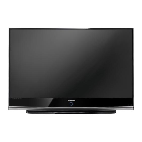
- Page 1 DLP TV Chassis : L70A(N)_Aquamarine Model : HL61A750A1FXZA HL67A750A1FXZA SERVICE Manual DLP TV CONTENTS 1. Precaution 2. Product Specification 3. Disassembly & Reassembly 4. Troubleshooting 5. Exploded View & Part List 6. Wiring Diagram 7. Schematic Diagram HL61A750A1F HL67A750A1F Refer to the service manual in the GSPN (see the rear cover) for the more information.
-
Page 2: Table Of Contents
4-3 Upgrade ..................................4-30 5. Exploded View & Part List 5-1 HL61A750A1FXZA Exploded View..........................5-1 5-2 HL67A750A1FXZA Exploded View..........................5-3 5-3 HL61A750A1FXZA Service Item ..........................5-5 5-4 HL67A750A1FXZA Service Item ..........................5-6 6. Wiring Diagram 6-1 Overall Wiring ................................6-1 7. Schematic Diagram 7-1 Circuit Description ...............................7-1 7-2 K880 Engine ................................7-2... -
Page 3: Safety Precautions
AC power cord for possible damages. Keep the part or the exceeds the specified limits, check each special part. lead away from any heat-emitting materials. 5. Warning for Engineering Changes: Never make any changes or additions to the circuit design or the internal part for this product. Samsung Electronics... - Page 4 11. Pay additional attention to the current leakage as the voltage between the power board and the ballast is 220 to 440V, i.e. very high. And also beware of possible electric shock from the primary power source. Samsung Electronics...
-
Page 5: Servicing Precautions
AC source and turn the switch on. Connect the insulating resistance meter (500V) to the AC plug blade. The insulating resistance between the blade of the AC plug and that of the conductive material should be more than 1 ㏁. Samsung Electronics... -
Page 6: Static Electricity Precautions
These servicing instructions are for use by qualified service personnel only. To reduce the risk of electric shock do not perform any servicing other than that contained in the operating instructions unless you are qualified to do so. Samsung Electronics... -
Page 7: Installation Precautions
4. Bend the external antenna cable when connecting it to the product. This is a measure to protect it from being exposed to moisture. Otherwise, it may cause a fire or electric shock. Samsung Electronics... - Page 8 MEMO Samsung Electronics...
-
Page 9: Product Specification
Composite L/R Input 1/2, S-Video L/R Input 1 Component1 Input L/R, Component2 Input L/R AUDIO input DVI Audio L/R PC Audio Input Audio Output Optical (SPDIF), Audio L/R Output Speaker Output 10W + 10W New Features Wiselink (USB2.0), 3D Ready, Anynet+ Samsung Electronics... - Page 10 - WISELINK (USB2.0) : This function enables you to view and play photo (JPEG) and audio files (MP3) through the TV’s WISELINK jack. - 3D/Dual-View : The HLT generation of Samsung DLP HDTVs are capable of displaying future 3D games, movies and other programming vis 3D compatible glasses and hardware.
-
Page 11: Specifications Analysis
Still Picture Wise Link Plug & Play S-Video In Rear 1 Rear 1 Rear 2 HDTV Component Video Input (Y, Pb, Pr) Rear 2 Rear 2 Rear 2 1080p/1080i/480P /480i/720P Connections HDMI Digital Sound Optical 1 Optical 1 Optical 1 BLUETOOTH Samsung Electronics... -
Page 12: Accessories
Accessories Item Item code Remark Remote Control BN59-00673A Batteries 4301-000103 Power Cord 3903-000144 Owner’s Instructions BP68-00658A Samsung Service center Warranty Card BN68-00872B Registration Card Safety Guide Manual AA68-03242L Cloth-Clean BN63-01798A HDMI/DVI cable HDMI Cable S-VIDEO Cable Antenna Cable Electronics Store/... -
Page 13: Disassembly & Reassembly
Description Photo ① Remove 10 screws to remove the back Back Cover bottom cover. :BH,+,B,M4,L12,ZPC(BLK),SWRCH18 ① Remove the Terminal Board by hands Terminal Board ① Remove 1 screw at the left side of Main Holder Chassis Assy. :BH,+,B,M4,L12,ZPC(BLK),SWRCH18 Samsung Electronics... - Page 14 ① Separate 10PIN DMD power cable, 2PIN Sub SMPS Wire and, 2 pin Inlet cable at the right side of Main Assy. ① Separate 12 pin Wire, and the Speaker wire at the left side of Main Assy. Samsung Electronics...
- Page 15 ① Pull out the holder Chassis. Side Holder Chassis direction. 3-1-2 Separation of the Main Board and Power Board (Disassembly is in reverse order of the assembly) Part Name Description Description Photo Main Assy ① Separate the 24PIN SMPS Wire, 1PIN GT Wire and. ① Remove 5 screws. :BH,+,-,S,M3,L6,ZPC(WHT), SWRCH18A ② Separate the SMPS Board. Samsung Electronics...
- Page 16 Disassembly & Reassembly Part Name Description Description Photo Main Assy ① Remove 4 screws. :PWH,+,B,M3,L10,ZPC(YEL), SWRCH18A ② Separate the Top Shield Case. ① Remove 1 screws. :PWH,+,B,M3,L10,ZPC(YEL), SWRCH18A ② Separate the Bottom Shield Case. Samsung Electronics...
- Page 17 ① Remove the 2 screw. : BH,+,B,M4,L12,ZPC(BLK),SWRCH18 ② Remove the engine by pulling it out of the cabinet. : Be careful when removing the Light Engine as it may get caught up by the upper cable of the case. Samsung Electronics...
- Page 18 ① Separate the 6PIN LED Power cable, Power 2PIN Sub SMPS Wire and 1PIN GT Board Wire. ① Remove 2 screws. :BH,+,B,M4,L12,ZPC(BLK),SWRCH18 ② Pull out the chassis. ① Remove the screws and detach the boards from the holder chassis. :PWH,+,-,B,M3,L10,ZPC(WHT), SWRCH18A,- Samsung Electronics...
- Page 19 Part Name Description Description Photo ① Separate the optical chassis from the Driver Cabinet. Board ② Remove the 2 screws. :BH,+,B,M4,L12,ZPC(BLK),SWRCH18 ③ Remove the Cover-P/J Lens from the Optical chassis. ① Separate the cables. ① Remove the FAN. Samsung Electronics...
- Page 20 Disassembly & Reassembly Part Name Description Description Photo ① Remove the 3 screws. Driver :PH,+,M4,L12,NI PLT,SWRCH18A,FP,- Board ① Remove the 4 screws. :PWH,+,-,B,M3,L6,ZPC(WHT), SWRCH18A,- Samsung Electronics...
- Page 21 Disassembly & Reassembly 3-1-6 Actuator (Smooth Picture) Replacement (Disassembly is in reverse order of the assembly) Part Name Description Description Photo ① Remove the cable at the Actuator. Actuator ① Remove the 3 screws. :BH,+,WSP,M3,L16,ZPC(WHT), SWRCH18A,-,- ① Replace it with a new actuator. ① Actuator, fixing bolts. Samsung Electronics...
- Page 22 Board. ② Separate the 8point Cables. ① Remove the 4 point screws. :PWH,+,-,M3,L30,NI PLT,SWRCH18A,UP,- ② After pushing the part of Spring_H/S DMD then separate it. ① Remove the 4 screws. :PWH,+,,B,M3,L6,ZPC(WHT), SWRCH18A,- ② Remove the Shield Case-DMD(R). 3-10 Samsung Electronics...
- Page 23 ① Remove the 4 point screws. Board :BH,+,M3,L12,NI PLT,SWRCH18A,-,- ② Remove the Bracket. : Don’t remove the 3 Yellow point screws ① Remove the DMD Board. Separate DMD Panel. DMD Panel DMD Panel DMD Panel ① DMD Board DMD Panel Samsung Electronics 3-11...
- Page 24 ① Separate the optical chassis from the Cabinet. ② Remove the 2 screws. :BH,+,B,M4,L12,ZPC(BLK),SWRCH18 ③ Remove the Cover-P/J Lens from the Optical chassis. ① Remove the 6 point screws. :BH,+,-,B,M3,L8,ZPC(BLK), SWRCH18A,- ② Separate the COVER-TOP. ① Remove the FAN. 3-12 Samsung Electronics...
- Page 25 Disassembly & Reassembly Part Name Description Description Photo ① Remove the FAN. ① Remove the 4 point screws of Heat Sink-Pipe and then Remove the Heat Sink-Pipe. ① Remove the BLUE LED. ① Remove the GREEN LED. Samsung Electronics 3-13...
- Page 26 Disassembly & Reassembly Part Name Description Description Photo ① Remove the RED LED. ① LED 3-14 Samsung Electronics...
- Page 27 REAR COVER-REAR and COVER-FRONT. disassembly : TH, M4, L15, BLK ① Separate 10 screws for fixing COVER-REAR, Bottom and COVER-FRONT. : TH, M4, L15, BLK ① Separate Bottom and COVER-REAR pull right and then take them off. Samsung Electronics 3-15...
- Page 28 Disassembly & Reassembly Part Name Description Description Photo ① After separating COVER-REAR and HOLDER- TERMINAL Bottom, separate HOLDER-TERMINAL. disassembly ① Remove 1 Screw CONNECTOR disassembly : TH, M4, L15, BLK ② Separate the 2 connectors from the main board 3-16 Samsung Electronics...
- Page 29 ② Separate 3 screws fixing disassembly BRKT-SCREEN : TH, M4, L12, YELLOW ① Remove the BRKT-SCREEN by BRACKET SCREEN pushing it toward the direction of the disassembly arrow. Left - Right Left - Right Left - Right Bottom Bottom Bottom Samsung Electronics 3-17...
- Page 30 Disassembly & Reassembly Part Name Description Description Photo ① Place your hand at the bottom center of SCREEN disassembly the screen then pick it up while pulling it towards you. ① Separate the screen in the COVER- FRONT. 3-18 Samsung Electronics...
- Page 31 ① Separate 1 screw for fixing COVER- COVER-DUST REAR and^pCOVER-DUST : BH,+,B,M4,L12,ZPC(BLK),SWRCH18 ② Push the indicating sign of the picture and separate SNAP of C/DUST from C/REAR. (Pushing part : the upper or lower part of jointing Screw) Samsung Electronics 3-19...
- Page 32 Disassembly & Reassembly Part Name Description Description Photo ③ Separate C/DUST with using the gap COVER DUST which occurs when^pSNAP of C/DUST is separated. ① Separate the screen in the COVER- FRONT. 3-20 Samsung Electronics...
-
Page 33: Troubleshooting
3. Check if there is an error in the main board. Check for a power signal from SMPS to other board see the schematic diagram. (7-3) And check for indicated power signal. MAIN SCREEN ATV, DTV, AV BAYHILL+ DDP3021 Panel MST336 Component CCLK HDMI OSD OK? DDP 3021 Pattern CHECK THE SCREEN CHECK THE SOURCE Main BOARD ERROR DMD BOARD ERROR Samsung Electronics... - Page 34 If necessary, replace DMD Board. Check Driver Power (CN9005) R9010 Gronding 16V OK? Check Sub SMPS (Pin 2/4/6) Operate driver in internal mode Replace driver (grounding R9010) LED On? Check Cables connected to DMD Board. If necessary, replace DMD Board. Samsung Electronics...
- Page 35 ■ Protect Status 1. Attempting to turn the LED ASSY on fails repeatedly If turning the LED on fails, the set automatically tries turning the LED ASSY on 3 times. If all attempts fail, all LED’s on the front panel will blink. Check the LED ASSY, LED Driver and the Sub power or SMPS and replace them if necesscary. Samsung Electronics...
- Page 36 Error in Rambus Dram (IC301) or the soldering. - Replace the DMD board Beehive mosaic patterns all over Error in the LVDS Receiver the screen (IC101,IC102) or the soldering. The H sync signals are not transferred to DDP3021. - Replace the DMD board. Samsung Electronics...
- Page 37 This disappears as the TV starts operating and the TV lamp gets brighter. However, you can avoid outside light by changing the position of the TV or the installation angle. Decreasing the illumination or changing the indoor lighting may work. 7. Screen Flip-over: Enter Factory mode in DDP3021 and perform H-Flip (flip horizontally) and V-Flip (flip vertically). The screen will flip over horizontally or vertically. Samsung Electronics...
-
Page 38: Adjustment
YYYY-MM-DD 3. DMD 0x00000001 indicates DMD board bit sequence program version. DMD XX, DSP-X-X-X DTP-LM-XXXX 4. Actuator Gain adjustment : See page 4-24. Date of Purchase : DD/MM/YYYY 5. Vertical / Horizontal Position adjustment : See page 4-21. 6. CCA : See page 4-22. 7. Board LED check : Check the LED is turned on. (In the DMD Board) 8. Tilt/Focus adjustment : See page 4-25 ~4-28. Samsung Electronics... - Page 39 MST336C DEFECT LOG BHP_DP Font Data Viewer Sharpness FBE3 LNA+ Expert Setting 4. Buttons operations within Service Mode MENU Full Menu Display / Move to Parent Menu Direction keys ▲/ ▼ Item Selection by Moving the Cursor Direction keys ◀ / ▶ Data Increase/Decrease for the Selected Item Source Cycles through the active input source that are connected to the unit Enter Item Selection/execution Samsung Electronics...
- Page 40 Control the Spread Spectrum. Controled by Engineer. SSC MRR Control the Spread Spectrum. Controled by Engineer. SSC MFR Control the Spread Spectrum. Controled by Engineer. SSC QLC Control the Spread Spectrum. Controled by Engineer. VISUAL TEST Enable/Disable Disable OSD is semitransparent on Disable Samsung Electronics...
- Page 41 Gamma Table Selection This displays the built-in pattern of the DDP3021 chip. DDP3021 drives the DMD panel, so displaying this pattern Test Pattern(DDP) 0~18 means there is no error in the DDP3021 projection function and the panel itself. Samsung Electronics...
- Page 42 [TI - COOL1] X 0.000~0.999 [TI - COOL1] Y 0.000~0.999 [TI - NORMAL] X 0.000~0.999 [TI - NORMAL] Y 0.000~0.999 [TI - WARM1] X 0.000~0.999 [TI - WARM1] Y 0.000~0.999 [TI - WARM2] X 0.000~0.999 [TI - WARM2] Y 0.000~0.999 TI Offset Adjust ON/OFF 4-10 Samsung Electronics...
- Page 43 Target Blue Y value for CCA [WARM1] DWhiteX 0 ~ 32766 Target Cyan X value for CCA [WARM1] DWhiteY 0 ~ 32766 Target Cyan Y value for CCA [WARM2] DWhiteX 0 ~ 32766 Target Magenta X value for CCA [WARM2] DWhiteY 0 ~ 32766 Target Magenta Y value for CCA Samsung Electronics 4-11...
- Page 44 0 - 1000 [sRGB] Blue-y 0 - 1000 [sRGB] Blue-y 0 - 1000 [sRGB] Cyan-y 0 - 1000 [sRGB] Magenta-x 0 - 1000 [sRGB] Magenta-y 0 - 1000 [sRGB] Yellow-x 0 - 1000 [sRGB] Yellow-y 0 - 1000 Over lap 0 ~ 2 4-12 Samsung Electronics...
- Page 45 Setting Brightness in Standard Mode Standard Sharpness 0~100 Setting Sharpness in Standard Mode Standard Color 0~100 Setting Color in Standard Mode Standard Tint 0~100 Setting Tint in Standard Mode Standard Backlight 0~10 Setting Backlight in Standard Mode Samsung Electronics 4-13...
- Page 46 Larger values increase 3D comb motion detection sensitivity to 3d_comb_chroma_sns chroma motion and noise Larger values decrease 3D comb motion detection sensitivity to 3d_comb_luma_core luma motion and noise Larger values increase 3D comb motion detection sensitivity to 3d_comb_luma_sns luma motion and noise cmd_gain_mts_ntsc 4-14 Samsung Electronics...
- Page 47 0~63 RED GAIN 0~255 GREEN GAIN 0~255 BLUE GAIN 0~255 SOGMID_CTRL 0~31 SEP_THR 0~255 PRECST 0~255 POSTCST 0~255 ADC_BWR 0~15 ADC_BWG 0~15 ADC_BWB 0~15 SOG_BW 0~255 D_R_offset 0~127 D_G_offset 0~127 D_B_offset 0~127 D_CALDLYC 0~255 D_SMPDLY 0~255 D_SMPDURC 0~255 CAL_CTRL0 0~255 Samsung Electronics 4-15...
- Page 48 Range Default Remark sharp75 0~100 Pre_GainH1 0~15 Pre_GainH2 0~15 Pre_GainV1 0~15 Pre_GainV2 0~15 Post_GainH1 0~15 Post_GainH2 0~15 Post_GainH3 0~15 Post_GainV1 0~15 Post_GainV2 0~15 CTI_Gain 0~15 Pre_LTIH 0~15 Pre_LTIV 0~15 Post_LTIH 0~15 Post_LTIV 0~15 CDataCoring Sub Color 0~80 4-16 Samsung Electronics...
- Page 49 0~255 M-Skin_UV 0~255 M-Sub Color 0~255 Sub Contrast 0~150 Sub Brightness 0~511 14. LNA+ Item Range Default Remark Off_NR_Gain 0~31 db0_NR_Gain 0~31 db1_NR_Gain 0~31 db2_NR_Gain 0~31 db3_NR_Gain 0~31 0~11 0~11 Medium 0~11 Hign 0~11 Auto 0~11 Still_Check Samsung Electronics 4-17...
- Page 50 Remark Black adjust off, Low, Mid, High Dynamic Contrast off, Low, Mid, High Gamma -3~3 Flesh tone -15~15 Edge Enhance off,On xvYCC … Inactive 17. Expert Gray Scale Item Range Default Remark R-Offset 0~50 G-Offset 0~50 B-Offset 0~50 R-GAIN 0~50 G-GAIN 0~50 B-GAIN 0~50 4-18 Samsung Electronics...
- Page 51 … Custom_Y_red … Custom_Y_green … Custom_Y_blue … 19. Expert Others Item Range Default Remark Size 4:3, 16:9, just scan Just Scan H-Positioin V-Positioin off, Low, Mid, High, auto Auto HDMI Black Level … Film Mode off, on Auto Motioin Plus off, Low, Mid, High Samsung Electronics 4-19...
- Page 52 Dynamic Global OnOff OFF/ ON Dynamic Local OnOff OFF/ ON Dynamic Skin OnOff OFF/ ON Dynamic Strength Low/Mid/Max Dynamic Cont Gain 0~100 Dynamic Satu OFF/ ON Dynamic Satu Gain 0~255 Sharp Picture OFF/ ON VLUT TBD0 Sharp Filter HD High Sharp Picture Gain 0~255 4-20 Samsung Electronics...
- Page 53 LED Clear Mute Time[RF] 0~1000ms 600ms Actu Gain[Patt1] 0~175 Actu Gain[Patt2] 0~175 Visual TEST 25. DEFECT LOG Item Range Default Remark Select Log Type DEFECT/NVRAM DEFECT VIEW LOG 26. Font Data Viewer You can see the font in the set. Samsung Electronics 4-21...
- Page 54 4-2-4 Service Adjustment ■ Vertical / Horizontal Position Adjustment 1. Turn off the power to put the unit into the STAND-BY mode. 2. In order to enter the Service Mode, press MUTE buttons on the remote control. POWER 3. Select “DDP3021” on the first display of the Service mode menu. 4. Select “H/V-Position” for vertical positioning and Horizontal positioning by using ▲/▼/◄/► the buttons. Press the (Up, Down, Left, Right) buttons to adjust the screen position. 4-22 Samsung Electronics...
- Page 55 1) This procedure is needed if the Main board, DMD Board,and light engine are changed. 2) Turn off power to put the unit into the STAND-BY mode. 3) In order to enter the Service Mode, press MUTE buttons on the remote POWER control. 4) Select “Option” on the display of the Service mode menu 5) If either the DMD or Light Engine is changed. Press the ▼ ▲ (Up or Down) button to move to Digital → DMD, then press ENTER to select. 6) Then Press ENTER to save CCA information to the DMD board. Samsung Electronics 4-23...
- Page 56 7) If the Main Board is changed, Press the ▼ ▲ (Up or Down) button to move to DMD → Digital, then press ENTER to select. 8) Then Press ENTER to save CCA information to the Main board * Attention Performing CCA is independent on current display’s resolution and input signal type if you don’t measure color coordinates data. Measuring color coordinates data requires specific equipment not possessed by service personnel, that makes performing manual adjustment impossible. Adjusting CCA is applied to all the signal mode. Don’t change desired value because it will be harmful to the color of the SET. 4-24 Samsung Electronics...
- Page 57 6) Press the ◀▶ (Left of Right) button to adjust. check the smooth picture at it’s minimum and maximum values of changing, then adjust to the mean value. - ACTUATOR GAIN [Patt 1], ACTUATOR GAIN [Patt 2] - ACTUATOR GAIN[Patt 1],ACTUATOR GAIN[Patt 2] Before Adjusting After Adjusting Actuator Gain 2. Making Adjustments 1) As shown in the picture above, change the actuator values to eliminate saw tooth shapes. - To fine tune, increase the data value ensuring that you get the center between the starting and ending points of the disappearing saw tooth shape. Samsung Electronics 4-25...
- Page 58 Troubleshooting 4-2-5 Replacements & Calibration ■ Tilt the Screen 1. Remove the 14 point screws. Remove the Bottom cover. 2. Loosen the 3 points screws. :TH,B,M4.L15,BLK,SWRCH18A *Left 2 points screws :PWH,S,M3,L8,ZPC(YEL),SWRCH18A *Right 1 points screw : PWH,S,M3,L7,ZPC(YEL),SWRCH18A 3. Turn off the power to put the unit into the STAND-BY mode. In order to enter the Service Mode, press “Mute” → “1” → “8” → “2” → “POWER” buttons on the Remote Control. Select “DDP3021 (LED)” on the first display of the Service Mode menu. Press the ▲ ▼ (Up or Down) buttons to select the test pattern option, then press ENTER to select. Press the ► (Right) button until you see the CROSSHATCH PATTERN. Then, adjust the screen position, by holding both of the upper corners of the DMD CROSSHATCH PATTERN board. CROSSHATCH PATTERN 4-26 Samsung Electronics...
- Page 59 3) Since the alignment is done from the rear use a mirror or a second person to confirm the adjustment is complete or remove the side port and view the screen through the port on the side for Focus Alignment. Samsung Electronics 4-27 Focus Alignment Focus Alignment...
- Page 60 Remote Control. Select “DDP3021” and enter the Test Pattern (DDP) Menu Press the ▲ ▼ (Up or Down) buttons, then press ENTER to select. Press the ▶ (Right) button until you see the Full White picture. 4. Upper knob is for the vertical illumination adjustment and the 3. Rotate the 2 points fine adjustment dials. lower knob is for the horizontal illumination adjustment. 4-28 Samsung Electronics...
- Page 61 ※ Until Full White pattern without the brindle is made in the Best Illumination situation, adjust the dials delicately. u l l u l l i t a i t a u l l u l l i t a i t a u l l u l l i t a i t a Samsung Electronics 4-29...
-
Page 62: Upgrade
It may take up to 30 seconds. Press the ◀ or ▶ button to select OK, then press the ENTER button. The upgrade starts. Please be careful to not disconnect the power or remove the USB drive while upgrades Software Upgrade are being applied. Upgrade version XXXX to version XXXX ? The The TV will shut off and turn on automatically after completing the firmware upgrade. system would be reset after upgrade. Please check the firmware version after the upgrades are complete. Cancel ※ The firmware and upgrade process may be different by country and region. T-AQMAUSC-XXXX T-AQMAUSM-XXXX EDID SUCCESS RFS : T-AQMAUSC-YYYYMMDD YYYY-MM-DD DMD XX, DSP-X-X-X DTP-LM-XXXX Date of Purchase : DD/MM/YYYY 4-30 Samsung Electronics... - Page 63 DMD XX, DSP-X-X-X DTP-LM-XXXX EPA Standard CHECKSUM Date of Purchase : DD/MM/YYYY BHP_VDEC SERVICE MST336C DEFECT LOG S/W Version BHP_DP Font Data Viewer Sharpness FBE3 LNA+ Expert Setting 2. Procedures for checking in the User Menu You can check the S/W Version using the customer menu using the following procedure. - Push the MENU button on remote control - Select Setup Menu - Select SW Upgrade - Push the INFO button on remote control Samsung Electronics 4-31...
-
Page 64: Exploded View & Part List
Exploded View & Part List 5. Exploded View & Part List 5-1 Exploded View HL61A750A1FXZA Samsung Electronics... - Page 65 S.N.A T0444 BP96-01753A ASSY BRACKET P-SCREEN SIDE -,61K8(LEFT), S.N.A T0444 BP96-01754A ASSY BRACKET P-SCREEN SIDE -,61K8(RIGHT) S.N.A T0445 BP96-01819A ASSY BRACKET P-SCREEN BOTTOM -,61K8,TOP, S.N.A T0445 BP96-01752A ASSY BRACKET P-SCREEN BOTTOM -,61K8,-,AL S.N.A T0507 BP63-00832A COVER-DUST 46K5(SLIM),PS,HB,BK500 S.N.A Samsung Electronics...
- Page 66 Exploded View & Part List 5-2 Exploded View HL67A750A1FXZA Samsung Electronics...
- Page 67 S.N.A T0444 BP96-02031A ASSY BRACKET P-SCREEN SIDE D750 67”(LEFT S.N.A T0445 BP96-02027A ASSY BRACKET P-SCREEN BOTTOM D750 67”(BO S.N.A T0445 BP96-02029A ASSY BRACKET P-SCREEN BOTTOM D750 67”(TO S.N.A T0507 BP63-00832A COVER-DUST 46K5(SLIM),PS,HB,BK500 S.N.A T0514 BP61-01631A BRACKET-SUPPORT 67A750,SECC,T1.2,NTR,BAC S.N.A Samsung Electronics...
- Page 68 T0053 BP67-00361A SCREEN FRESNEL CITRINE,1.9T,61W, 1372mm T0054 BP67-00344A SCREEN LENTI Laurel,1.7T,61W, 1372mm x 7 PEARL,TM96A,49,USA,SAMSUNG,TOOL T0074 BN59-00673A REMOCON T0159 BP96-01726B ASSY PCB P-SMPS Aquamarin,LED DLP TV,DC2 T0175 BP96-01794A ASSY SPEAKER P 8ohm,Horn type,10W,1100/4 T0764 BP44-01001A SMPS-DLP TV PN082DPS-VF(A),AC/DC,90V-132 Samsung Electronics...
- Page 69 Exploded View & Part List 5-4 Service Item HL67A750A1FXZA ※ This is the list which is available to repair the real material at the time of service. Loc. No. Code No. Description Specification Q’ty SA/SNA Remark M0013 BP96-02025A ASSY COVER P-REAR D750 67”...
- Page 70 MEMO Samsung Electronics...
-
Page 71: Wiring Diagram
FAN 2 FAN 3 CN805 CN800 CN9005 CN9007 CN1002 CN102 CN801 CN101 LED Driver SUB SMPS Color Actuator Sensor CN702 CN1301 CN101 CN811 CN801 CN201 PD801S CN701 GT805 GT601 MAIN SMPS MAIN CN000 SPEAKER CN101 INDICATOR KEY CONTROL Samsung Electronics... - Page 72 BP39-00255A BP39-00180D BP39-00174J Photo ⑦ Inlet ⑧ Ballast cable ⑨ Main to DMD cable Code BP96-02046A BP39-00247A BP39-00274B Photo ⑩ LVDS(350mm) ⑪ Sub Power ⑫ 22P 300mm Cable Code BP96-01970C BP39-00297A BP39-00299A Photo ⑬ LVDS(350mm) Code BP96-01970C Photo Samsung Electronics...
- Page 73 PIN No. Signal STB5V Main(CN701) ↔ LED INDICATOR(CN1) PIN No. Signal BLEU_LED 16VB POWER_SW STB5V LAMP_GRN TIMER_GRN 16VB STB_RED POWER_SW KEY1 KEY2 5.7VB 5.7VB STB_5V 12VB 12VB LED INDICATOR(CN2) ↔ KEY CONTROL(CN101) 12VB PIN No. Signal 12VB P_ACTOUT 12VB Samsung Electronics...
- Page 74 MAIN(CN1301) ↔ DMD(CN1002) PIN No. Signal PIN No. Signal LVDS_E_TX0- 3D_SIGNAL LVDS_E_TX0+ LVDS_E_TX1- LAMP_ERROR LVDS_E_TX1+ LVDS_E_TX2- LVDS_E_TX2+ LVDS_E_TXCLK- LVDS_O_TX0- LVDS_E_TXCLK+ LVDS_O_TX0+ LVDS_E_TX3- LVDS_O_TX1- LVDS_E_TX3+ LVDS_O_TX1+ LVDS_E_TX4- LVDS_O_TX2- LVDS_E_TX4+ LVDS_O_TX2+ LVDS_O_TXCLK- SCL_DMD LVDS_O_TXCLK+ SDA_DMD LVDS_O_TX3- LVDS_O_TX3+ DDP_READY LVDS_O_TX4- PWR_GOOD LVDS_O_TX4+ nLVDS_EN Samsung Electronics...
- Page 75 Wiring Diagram SUB SMPS(CN801) ↔ DMD(CN805) ↔ LED DRIVER(CN9007) LED DRIVER(CN9005) PIN No. Signal PIN No. Signal LED_SENS LED_B LED_G LED_R LED_SUBFRAME LED_LAMPLITZ N.C. LED_EN LED_DRV_DOUT DMD(CN805) ↔ Color Sensor(CN1) LED_DRV_DIR PIN No. Signal LED_DRV_DIN LED_DRV_OE Sensor_RST LED_DRV_SCLK RGB_SENSE Samsung Electronics...
- Page 76 This transfers the image data to DMD Board. Sub Power Supply Power to LED Driver 22P 300mm Transfers I2C signal and LED Control Signal to LED Driver. And transfers Power. 5P 200mm Transfers Power and signal to Color Sensor. Samsung Electronics...
-
Page 77: Schematic Diagram
The LED Driver board is like a stabilizer for lighting the LED light source. The ultimate purpose of the TV set is to project an image onto the screen and output the voice signals synchronized with the image. Samsung Electronics... -
Page 78: K880 Engine
▶ Color Sensor : checks the color passing in the illuminance part, then feedback the color status to the LED Driver. ▶ DMD Board : makes a screen data, received from Main board, as a real screen in the DMD panel. Samsung Electronics... - Page 79 Schematic Diagram 7-3 Schematic Diagram 7-3-1 Main Board-1 This Document can not be used without Samsung’s authorization. Power Samsung Electronics...
- Page 80 Schematic Diagram 7-3-2 Main Board-2 This Document can not be used without Samsung’s authorization. Power C380 1UF 6.3V VIDEO1_SR_IN C381 1UF 6.3V VIDEO1_SL_IN C382 1UF 6.3V VIDEO2_SR_IN C383 1UF 6.3V VIDEO2_SL_IN C384 1UF 6.3V COMP1_SR_IN C385 1UF 6.3V COMP1_SL_IN C386 1UF 6.3V...
- Page 81 Schematic Diagram 7-3-3 Main Board-3 This Document can not be used without Samsung’s authorization. Power FROM TERMINAL BLOCK USB2.0 5VB_3D_IR B3.3V 100OHM R358 SVHS1_IDENT R470 33OHM BD301 3.3UH SVHS1_C_BAY L314 R360 33OHM SVHS1_Y_BAY R326 IC406 10KOHM SP619EK-L/TR VOUT R324 3D_PW_EN ENABLE...
- Page 82 Schematic Diagram 7-3-4 Main Board-4 This Document can not be used without Samsung’s authorization. Power DDC_VCC DDC_VCC TP507 DDC_WP DDC_WP D407 D412 D440 100NF IC401 IC404 MMBD4148SE MMBD4148SE MMBD4148SE MMBD4148SE 24LC02B-E/SN 24LC02B-E/SN 10UF 10UF 100NF HDMI1_5V HDMI2_5V R419 R460 47OHM 47OHM...
- Page 83 Schematic Diagram 7-3-5 Main Board-5 This Document can not be used without Samsung’s authorization. Power HDMI1_DDC_SDA HDMI1_DDC_SCL HDMI1_RXCLK- HDMI1_RXCLK+ HDMI1_RX0- HDMI1_RX0+ HDMI1_RX1- HDMI1_RX1+ HDMI1_RX2- HDMI1_RX2+ HDMI2_RXCLK- HDMI2_RXCLK+ HDMI2_RX0- HDMI2_RX0+ HDMI2_RX1- HDMI2_RX1+ HDMI2_RX2- HDMI2_RX2+ HDMI3_RXCLK- HDMI3_RXCLK+ HDMI3_RX0- HDMI3_RX0+ HDMI3_RX1- HDMI3_RX1+ HDMI3_RX2- HDMI3_RX2+...
- Page 84 Schematic Diagram 7-3-6 Main Board-6 This Document can not be used without Samsung’s authorization. Power ATSC HALF NIM TUNER TU33V_NIM B5V_TUNER TP602 BD602 3.3UH C609 C610 TP601 100NF BD601 TU601 TU33V 3.3UH FGND FGND TDQU2-K01A TP610 MGND1 C601 MGND2 R611 AGC_NIM...
- Page 85 Schematic Diagram 7-3-7 Main Board-7 This Document can not be used without Samsung’s authorization. Power FROM IR/LED/CONTROL PCB CONNECTOR WITH DMD POWER AND ETC POWER CHECK INDICATOR LED B3.3V MP DELETE B12V MICOM DEBUG A3.3V BD701 BEAD_CHIP A2008WVO-10P BD703 JE200-AIT-NP-13 2KOHM 100NF A3.3V...
- Page 86 Schematic Diagram 7-3-8 Main Board-8 This Document can not be used without Samsung’s authorization. Power UART PORT FOR SVC & DEBUGGING A3.3V A3.3V A3.3V BD801 BD802 BD803 R809 R810 10KOHM 10KOHM R801 R802 C801 10KOHM 10KOHM 100NF C802 100NF C803 10UF...
- Page 87 Schematic Diagram 7-3-9 Main Board-9 This Document can not be used without Samsung’s authorization. Power TU_SIF_BAY OPTION R901 C904 R902 C929 62OHM 100NF 62OHM 100NF TU_CVBS TU_CVBS_BAY TU_SIF TU_SIF_BAY C901 C902 C924 C925 33PF 33PF 33PF 33PF B3.3V CML_CH C950 C954...
- Page 88 Schematic Diagram 7-3-10 Main Board-10 This Document can not be used without Samsung’s authorization. Power B3.3V PLL_FLT_AUDA PLL_FLT_AUDB C1001 C1005 B3.3V 1.8NF 1.8NF B3.3V R1034 1KOHM R1092 CN1001 4.7KOHM SLAN_INT0 cn_s_008_g2 KTC3875S-Y 0OHM R1085 TRST PLL_FLT_VID PLL_FLT_SSVID SLAN_INT Q1001 JTRST MGND1 R1086...
- Page 89 Schematic Diagram 7-3-11 Main Board-11 This Document can not be used without Samsung’s authorization. Power Signal B1.8V B1.8V C1101 C1102 C1104 C1107 C1109 C1111 C1113 C1116 C1118 C1121 C1125 C1126 C1127 C1128 C1129 C1130 C1131 C1132 C1133 C1134 100NF 100NF 100NF 100NF...
- Page 90 Schematic Diagram 7-3-12 Main Board-12 This Document can not be used without Samsung’s authorization. Power Signal B3.3V S4LJ003X IC1001 AP33 R12102 R1286 22OHM PCIAD_0 CANSM AN33 R1287 22OHM 4.7KOHM PCIAD_1 NOCNT AN28 R1288 22OHM PCIAD_2 ONENAND_CLK FLEX_CLK AP34 R1289 22OHM PCIAD_3 SMWAIT...
- Page 91 Schematic Diagram 7-3-13 Main Board-13 This Document can not be used without Samsung’s authorization. Power FI-RE41S-VF FGND IC1001 S4LJ003X MGND1 MGND3 R1308 DVICLK 0OHM FGND DVI_CLK LCD_ODD_TX0- TAN0 AA32 R1309 DVIHSYNC 0OHM DVI_HSYNC LCD_ODD_TX0+ 3D_SIGNAL TAP0 AA33 R1310 DVIVSYNC 0OHM FGND MST_ROUT<0..9>...
- Page 92 Schematic Diagram 7-3-14 Main Board-14 This Document can not be used without Samsung’s authorization. Power B3.3V_1 B3.3V_1 B1.2V B1.2V_CORE S4LJ003X C1410 C1417 C1423 C1430 C1436 C1442 C1448 C1453 C1458 IC1001 B3.3V 100NF 100NF 100NF 100NF 100NF 100NF 100NF 100NF 100NF VDDI_1 VDDOP_1...
- Page 93 Schematic Diagram 7-3-15 DMD Board-15 This Document can not be used without Samsung’s authorization. R100 R101 R102 R103 R104 R105 100OHM 100OHM 100OHM P3P3V CN1002 100OHM 100OHM 100OHM LVDS_O_RX0- FI-RE41S-VF LVDS_O_RX0+ LVDS_O_RX1- MGND1 LVDS_O_RX1+ L100 MGND11 MGND3 LVDS_EN LVDS_O_RX2- POWERGOOD LVDS_O_RX2+ ASIC_READY...
- Page 94 Schematic Diagram 7-3-16 DMD Board-16 This Document can not be used without Samsung’s authorization. DDP3021 I/O IC200 DDP3021 DDA_P<0:15> AL16 P1_WCLK P1_WCLK DDA_P_0 AN16 P1_DATAEN P1_DATAEN DDA_P_1 AN15 P1_HSYNC P1_HSYNC DDA_P_2 AM14 P1_VSYNC P1_VSYNC DDA_P_3 AP14 P1_B_CB<0:9> DDA_P_4 AM13 P1_A_0 DDA_P_5 AP13...
- Page 95 Schematic Diagram 7-3-17 DMD Board-17 This Document can not be used without Samsung’s authorization. RLD_VTT P1P5V RLDRAM RLD_VREF IC200 RLD_VTT P1P5V DDP3021 IC301 RLD_QVLD RLDRAM_QVLD R311 VDDQSNS RLD_QK1_N RLDRAM_QK1_N 100OHM VLDOIN RLD_QK1_P RLDRAM_QK1_P IC302 RLD_QK0_N R310 RLDRAM_QK0_N MT49H8M36HT-TI PGND 10KOHM RLD_QK0_P RLDRAM_QK0_P...
- Page 96 Schematic Diagram 7-3-18 DMD Board-18 This Document can not be used without Samsung’s authorization. DAD2000 P3P3V IC400 BD401 AD7801BRU C405 C406 ACT_CTL<0:8> 27PF 27PF X400 DGND P_ACTOUT C402 C403 C404 25.0MHZ VOUT P2P5V 100NF 100NF 10NF AGND IC401 C401 C400 REFIN DO NOT INSTALL...
- Page 97 Schematic Diagram 7-3-19 DMD Board-19 This Document can not be used without Samsung’s authorization. FLASH/GPIO P3P3V P3P3V C520 100NF IC200 DDP3021 PM_DATA<0:15> PM_ADDR<0:21> M_ASIC_CFG0 GPIO_0 PM_DATA_0 C500 C501 C502 M_ASIC_CFG1 DO NOT INSTALL 0OHM GPIO_1 PM_DATA_1 100NF 100NF 10UF R531 M_ASIC_CFG2 SCI_TXD...
- Page 98 Schematic Diagram 7-3-20 DMD Board-20 This Document can not be used without Samsung’s authorization. P3P3V VCC33 IC200 BD600 DDP3021 AM33 DDP3021 POWER AP32 C600 C601 C612 C602 C603 C604 C605 C606 C607 C608 C609 C610 C611 AP28 100NF 100NF 10UF 100NF 100NF...
- Page 99 Schematic Diagram 7-3-21 DMD Board-21 This Document can not be used without Samsung’s authorization. PMD1000 P3P3V R750 R751 R752 R753 R754 10KOHM 10KOHM 10KOHM 10KOHM 10KOHM IC750 PMD1000 PWR_GOOD SSP0_CSZ_0 PWRGOOD SSP0_CLK POSENSE SSP0_RXD POSENSE DOUT SSP0_TXD PMDINTZ PMDINTZ F1SW P12V F2SW...
- Page 100 Schematic Diagram 7-3-22 DMD Board-22 This Document can not be used without Samsung’s authorization. P2P5V P2P5V P2P5V P3P3V DO NOT INSTALL R800 R801 R802 R803 R804 R805 R806 TP_GND0 10KOHM 10KOHM 10KOHM 10KOHM 10KOHM 10KOHM 10KOHM TP_2P5 TP_TRSTZ TRSTZ TP_TDI TP_TMSARM TMSARM...
- Page 101 Schematic Diagram 7-3-23 DMD Board-23 This Document can not be used without Samsung’s authorization. (+3.3V) VCC_DMD IC900 PL22323-1640-01F (+8V) VCC2_DMD READOUTA0 READOUTA1 BIST_A VCC2 RESERVED_TS BIST_B VCC2 VCC2 SSP1_CLK SCPCLK MBRST00 VCC2 SSP1_TXD SCPDI MBRST01 VCC2 SSP1_RXD SCPDO MBRST02 VCC2 SSP1_CSZ_0 nSCPEN...
- Page 102 Schematic Diagram 7-3-24 DMD Board-24 This Document can not be used without Samsung’s authorization. PULL UP & DOWN P3P3V R1003 0OHM 0OHM R1005 R1000 100KOHM LED_DRV_DIR 0OHM R1007 R1001 100KOHM DSP_GPIO31 R1002 100KOHM LED_SENS_SCLK R1004 100KOHM LED_SENS_OE C1000 C1001 100NF 100NF R1006...