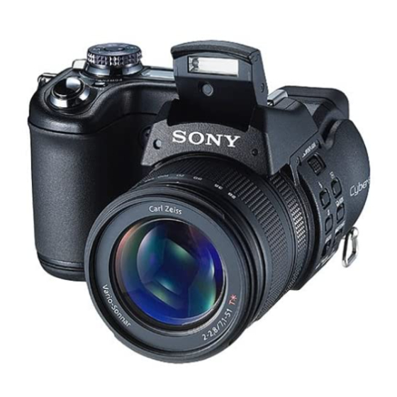
Sony DSC-F828 Service Manual
Digital still camera
Hide thumbs
Also See for DSC-F828:
- Service manual (287 pages) ,
- Operating instructions manual (160 pages) ,
- Adjustment (85 pages)
Table of Contents
Advertisement
SERVICE MANUAL
Ver 1.1 2004. 04
Revision History
Revision History
How to use
How to use
Acrobat Reader
Acrobat Reader
Link
Link
SPECIFICATIONS
SPECIFICATIONS
SERVICE NOTE
SERVICE NOTE
DISASSEMBLY
DISASSEMBLY
• For ADJUSTMENTS (SECTION 6), refer to SERVICE MANUAL, ADJ (987627951.pdf).
• For INSTRUCTION MANUAL, refer to SERVICE MANUAL, LEVEL 1 (987627941.pdf).
• Reference No. search on printed wiring boards is available.
• When the laser unit is repaired,
Make sure to follow the items of "NOTE ON HANDLING THE LASER DIODE".
On the SY-096 board
This service manual provides the information that is premised the circuit board replacement service and not intended repair
inside the SY-096 board.
Therefore, schematic diagram, printed wiring board, mounted parts location and electrical parts list of the SY-096 board are not
shown.
The following pages are not shown.
Schematic diagram ............................. Pages 4-25 to 4-44
Printed wiring board ............................ Pages 4-59 to 4-62
DSC-F828
BLOCK DIAGRAMS
BLOCK DIAGRAMS
FRAME SCHEMATIC DIAGRAMS
FRAME SCHEMATIC DIAGRAMS
SCHEMATIC DIAGRAMS
SCHEMATIC DIAGRAMS
Mounted parts location ............................. Pages 4-65 to 4-66
Electrical parts list ................................... Pages 5-14 to 5-18
US Model
Canadian Model
AEP Model
UK Model
Hong Kong Model
Australian Model
Korea Model
Tourist Model
Chinese Model
Japanese Model
PRINTED WIRING BOARDS
PRINTED WIRING BOARDS
REPAIR PARTS LIST
REPAIR PARTS LIST
DIGITAL STILL CAMERA
2
LEVEL
E Model
Advertisement
Chapters
Table of Contents

Related Manuals for Sony DSC-F828


Summary of Contents for Sony DSC-F828
- Page 1 DSC-F828 SERVICE MANUAL LEVEL US Model Ver 1.1 2004. 04 Canadian Model Revision History Revision History AEP Model UK Model How to use How to use E Model Acrobat Reader Acrobat Reader Hong Kong Model Australian Model Korea Model Tourist Model...
-
Page 2: Specifications
DSC-F828 SPECIFICATIONS x Camera [LCD screen] x AC-L15A/L15B AC Adaptor [System] LCD panel used Power requirements AC 100 − 240 V, 50/60 Hz 4.6 cm (1.8 type) TFT drive Image device 11 mm (2/3 type) color Total number of dots Current consumption 134 400 (560×240) dots... - Page 3 CRITIQUES POUR LA SÉCURITÉ DE FONCTIONNEMENT. NE COMPONENTS WITH SONY PARTS WHOSE PART NUMBERS REMPLACER CES COMPOSANTS QUE PAR DES PIÈSES SONY APPEAR AS SHOWN IN THIS MANUAL OR IN SUPPLEMENTS DONT LES NUMÉROS SONT DONNÉS DANS CE MANUEL OU PUBLISHED BY SONY.
-
Page 4: Table Of Contents
DSC-F828 TABLE OF CONTENTS SERVICE NOTE • AS-050 FLEXIBLE SCHEMATIC DIAGRAM ···························· 4-14 1-1. NOTE FOR REPAIR ······················································· 1-1 • UA-003 (AV, USB JACK) 1-2. DISCHARGING OF THE FLASH UNIT’S CHARGING SCHEMATIC DIAGRAM ···························· 4-15 CAPACITOR ··································································· 1-1 • LB-091 (EVF, EVF BACK LIGHT) 1-2-1. - Page 5 DSC-F828 5-1-5. BTH BLOCK ASSEMBLY ············································· 5-7 5-1-6. CABINET (REAR) BLOCK ASSEMBLY ····················· 5-8 5-1-7. EVF ASSEMBLY ···························································· 5-9 5-2. ELECTRICAL PARTS LIST ········································ 5-10 SY-096 Parts list of the board are not shown. Pages from 5-14 to 5-18 are not shown.
-
Page 6: Service Note
There is a danger of electric shock by this high voltage when the capacitor is handled by hand. The electric shock is caused by the charged voltage which is kept without discharging when the main power of the DSC-F828 is simply turned off. Therefore, the remaining voltage must be discharged as described below. -
Page 7: Notes On Handling The Laser Diode
• The type of memory stick that cannot be Replace the memory stick. used by this machine, is inserted. C:13:01 MEDIA ERROR Format the memory stick with the DSC-F828. • Data is damaged. • Unformatted memory stick is inserted. Flash LED Checking of flash unit or replacement of... -
Page 8: Disassembly
DSC-F828 SECTION 2 HELP HELP DISASSEMBLY The following flow chart shows the disassembly procedure. DISASSEMBLY HELP HELP DISASSEMBLY DISASSEMBLY HELP Discharging the Capacitor DISASSEMBLY DISASSEMBLY HELP HELP HELP DISASSEMBLY DISASSEMBLY DISASSEMBLY SY-096 board service position HELP HELP HELP DISASSEMBLY DISASSEMBLY... -
Page 9: Cabinet (Lr) Assembly, Sw-410 Board
DSC-F828 NOTE: Follow the disassembly procedure in the numerical order given. 2-1. CABINET (LR) ASSEMBLY, SW-410 BOARD Caution Tape (A) Note: When installing, be careful not to pinch the extra length of flexible board because it can be easily pinched during installation. -
Page 10: Stroboscope Block Assembly
DSC-F828 2-2. STROBOSCOPE BLOCK ASSEMBLY 2 Peel the Radiation sheets (LR) from flexible boards. Dowel 1 Tapping screw Caution (M1.7 × 4) Radiation sheet (LR) Tapping screw Harness processing (M1.7 × 4) ST-088 board harness 8 Two screws (PT132) Note: Be careful not to drop (M2 ×... -
Page 11: St Section
DSC-F828 2-3. ST SECTION 5 ST section 1 Two screws (M2 × 4), 2 LS-067 board lock ace (6P) 3 SI-037 board (26P) 4 MT-067 board (16P) 2-4. ST-088 BOARD, LENS SECTION 8 Lens section 5 FP-750 flexible board (22P) -
Page 12: St Cabinet Assembly
DSC-F828 2-5. ST CABINET ASSEMBLY 2 Tapping screw (M1.7 × 4) 3 ST blind cover 4 Four tapping screws (M1.7 × 4) 6 ST section 1 AS-050 flexible board 5 ST cabinet assembly (10P) 2-6. MT-067 BOARD 1 Three tapping screws (M1.7 ×... -
Page 13: Board, Flash Unit
DSC-F828 2-7. SI-037 BOARD, FLASH UNIT Remove the ST unit holder from the SI-037 board by disengaging the claw while sliding the (A) section of the SI-037 board in the direction of the arrow (B). 5 ST cover SI-037 board... -
Page 14: Board, Laser Unit
DSC-F828 2-8. LS-067 BOARD, LASER UNIT 1 Tapping screw (M1.7 × 4) Two dowels 4 ST laser holder Two grooves 5 Remove the 6 Laser unit (D001) three solderings 7 LS-067 board Caution When soldering the laser unit on the LS-067 board, observe the following things. -
Page 15: Rear Cabinet Block Assembly
DSC-F828 2-9. REAR CABINET BLOCK ASSEMBLY (M2 × 5 Screw 4), lock ace Caution The LB-091 board may be damaged if you remove the rear cabinet block assembly forcibly. Be very careful not to damage the flexible board. (M2 ×... -
Page 16: Control Switch Block (Under)
DSC-F828 2-11.CONTROL SWITCH BLOCK (UNDER) 3 Block light guide plate (6P) Cabinet (rear) assembly Caution 4 LCD module (24P) Control switch block (mid)(10p) Control switch block (under) Control switch block (under) Tape (A) Caution 1 Three screws (M1.7 × 3),... -
Page 17: Bth Section
DSC-F828 2-13.BTH SECTION Caution Note: When installing, be careful not to pinch the flexible board or harness during installation. 6 Harness (microphone) 4 Control switch block (top) 7 Harness (speaker) (12P) 1 FP-754 flexible board 5 LCD module (26P) (21P) -
Page 18: Board
DSC-F828 2-14.SY-096 BOARD 2 FP-749 flexible board (10P) 4 FP-756 flexible board (51P) 6 SY-096 board 3 FP-748 board (60P) 5 Cushion (SY) screws (M1.7 × 3), 1 Two lock ace Caution Cushion (SY) SY-096 board 2-11... - Page 19 DSC-F828 2-15.DD-204 BOARD Caution Note: The power supply capacitor of the flash unit is charged to the high tension voltage as high as 300 V at a maximum. You will get electrical shock when you touch the terminal of the charged capacitor . The charged potential remains even after the main power of the machine is turned off.
-
Page 20: Lr-018 Board, Lithium Battery
DSC-F828 2-17.LR-018 BOARD, LITHIUM BATTERY 2 Two claws 4 Remove soldering from the two points. 3 LR-018 board (M1.7 × 4) 1 Tapping screw 5 Lithium battery 2-18.MEMORY STICK CONNECTOR 2 Hook 4 FP-749 flexible board (10P) 5 Memory stick connector... -
Page 21: Dc-In Connector, Ua-003 Board
DSC-F828 2-19.AJ-007 BOARD Screws (M1.7 × 3), lock ace 2 AJ-006 flexible board 3 AJ-007 board (6P) 2-20.DC-IN CONNECTOR, UA-003 BOARD Jack holder assembly 4 Three Claws 3 Two tapping screws (M1.7 × 4) 5 UA-003 board 6 Jack ground plate... -
Page 22: Fp-747/746/754 Flexible Board
DSC-F828 2-21.FP-747/746/754 FLEXIBLE BOARD FP-754 flexible board Caution 1 Ferrite core Tape (A) 2 harness (PT132) 3 Screw (M1.7 × 3), lock ace Radiation sheet (LR) FP-747 flexible board 6 Two screws (M1.7 × 3), Flexible guide (R) lock ace... -
Page 23: Hinge/Cabinet (Ll) Assembly
DSC-F828 2-22.HINGE/CABINET (LL) ASSEMBLY Hinge /Cabinet (LL) Assembly Remove it while rotating the Hinge/Cabinet (LL) Assembly. screws(2 × 4), 2 Two lock ace 1 Rotate the Hinge/Cabinet (LL) Assembly up to the position where screw becomes visible. 2-23.SPEAKER/MICROPHONE SECTION Harness processing screws (M1.7 ×... - Page 24 DSC-F828 2-24.CABINET UPPER ASSEMBLY (M1.7 × 4) 4 Three tapping screws Notch Control switch block (top), LCD module section screws (M1.7 × 3), 1 Two lock ace 6 MD cushion Cabinet upper section Control switch block (top) Caution When installing it, align the switch position Cabinet upper assembly as shown.
-
Page 25: Cabinet Upper Assembly
DSC-F828 [SERVICE POSITION (SY-096 BOARD) ] FP-756 flexible board (51P) FP-749 flexible board (10P) Control switch block (top) (12P) Memory stick connector CN709 CN451 SY-096 board Control switch block (under) (50P) CN706 CN711 CN701 CN751 FP-746 flexible board (51P) CN703... - Page 26 DSC-F828 2-25.CONTROL SWITCH BLOCK (TOP) 3 LCD panel Two claws Caution Control switch block (top) Tape (A) Tape (A) Control switch block (top) 2-19...
- Page 27 DSC-F828 2-26.CIRCUIT BOARDS LOCATION CF-097 DD-204 SY-096 ST-088 UA-003 SW-410 AJ-007 Board Name Function CAMERA DSP, CAMERA SYSTEM CONTROL, CF DRIVE I/F, USB I/F, MODE CONTROL, SY-096 AUDIO AMP, LCD DRIVER, EVF, LCD DRIVER, CONNECTOR, POWER SUPPLY AV, USB JACK...
-
Page 28: Control Switch Block (Top)
DSC-F828 2-27.CIRCUIT BOARDS AND FLEXIBLE BOARDS LOCATION Control switch block (top) Control switch block (under) FP-748 FP-749 (flexible) SI-037 LR-018 FP-754 FP-746 (flexible) (flexible) AJ-006 FP-751 (flexible) (flexible) Control switch block (mid) FP-756 (flexible) LB-091 LS-067 MT-067 FP-747 (flexible) FP-750... -
Page 29: Front Cabinet Section
DSC-F828 2003. 12. 8 Update HELP Sheet attachment positions and procedures of processing the flexible boards/harnesses are shown. STROBOSCOPE SECTION CABINET (LR) SECTION Tape (A) Tape (A) SW-410 board Control switch block (top) FP-751 flexible board FRONT CABINET SECTION FP-747 flexible board... - Page 30 DSC-F828 BTH SECTION CF radiation sheet (B) CF radiation sheet (A) SY-096 board Cushion (SY) BT holder assembly (front side) BT holder assembly (rear side) Tape (A) Ferrite bead DD-204 board Sheet (MS) Memory stick connector Fuse replacement caution label...
-
Page 31: Block Diagrams
DSC-F828 3. BLOCK DIAGRAMS Link Link OVERALL BLOCK DIAGRAM (1/3) POWER BLOCK DIAGRAM (1/2) OVERALL BLOCK DIAGRAM (1/3) POWER BLOCK DIAGRAM (1/2) OVERALL BLOCK DIAGRAM (2/3) POWER BLOCK DIAGRAM (2/2) OVERALL BLOCK DIAGRAM (2/3) POWER BLOCK DIAGRAM (2/2) OVERALL BLOCK DIAGRAM (3/3) - Page 32 DSC-F828 SECTION 3 3. BLOCK DIAGRAMS 3. BLOCK DIAGRAMS BLOCK DIAGRAMS 3-1. OVERALL BLOCK DIAGRAM (1/3) ( ) : Number in parenthesis ( ) indicates the division number of schematic diagram where the component is located. LENS UNIT (1/3) FP-756...
- Page 33 DSC-F828 3. BLOCK DIAGRAMS 3. BLOCK DIAGRAMS ( ) : Number in parenthesis ( ) indicates the division number of schematic diagram where the component is located. 3-2. OVERALL BLOCK DIAGRAM (2/3) AJ-006 SY-096 BOARD (2/3) LENS UNIT (2/3) AJ-007 BOARD...
- Page 34 DSC-F828 3. BLOCK DIAGRAMS 3. BLOCK DIAGRAMS 3-3. OVERALL BLOCK DIAGRAM (3/3) ( ) : Number in parenthesis ( ) indicates the division number of schematic diagram where the component is located. SY-096 BOARD (3/3) CONTROL SWITCH CONTROL SWITCH SW-410 BOARD...
- Page 35 DSC-F828 3. BLOCK DIAGRAMS 3. BLOCK DIAGRAMS ( ) : Number in parenthesis ( ) indicates the division number of schematic diagram where the component is located. 3-4. POWER BLOCK DIAGRAM (1/2) DD-204 BOARD Q401,402,407,T401 F001 CN401 STRB UNREG HIGHT VOLTAGE...
- Page 36 DSC-F828 3. BLOCK DIAGRAMS 3. BLOCK DIAGRAMS 3-5. POWER BLOCK DIAGRAM (2/2) ( ) : Number in parenthesis ( ) indicates the division number of schematic diagram where the component is located. FP-756 FP-749 SY-096 BOARD (3/3) FLEXIBLE FLEXIBLE CN103...
- Page 37 DSC-F828 4-2. SCHEMATIC DIAGRAMS 4-2. SCHEMATIC DIAGRAMS 4-3. PRINTED WIRING BOARDS 4-3. PRINTED WIRING BOARDS SECTION 4 PRINTED WIRING BOARDS AND SCHEMATIC DIAGRAMS 4-1. FRAME SCHEMATIC DIAGRAM (1/4) D001 Infrared ray emitter CN505 IR_LED_A IR_LED_K N.C. N.C. CN501 N.C. STRB_POPUP+...
-
Page 38: Frame Schematic Diagram (1/4)
DSC-F828 4-2. SCHEMATIC DIAGRAMS 4-2. SCHEMATIC DIAGRAMS 4-3. PRINTED WIRING BOARDS 4-3. PRINTED WIRING BOARDS FRAME SCHEMATIC DIAGRAM (2/4) REG_GND REG_GND REG_GND REG_GND REG_GND XFE_CS XCAM_SCK CAM_SO MF_OUT_F0 XCAM_RST MF_VCC XTG_CS MF_OUT_F1 XCDS_CS MF_GND CAM_SI SHUTTER+ EXT_STRB_CONT SHUTTER+ REG_GND SHUTTER-... -
Page 39: Frame Schematic Diagram (2/4)
DSC-F828 4-2. SCHEMATIC DIAGRAMS 4-2. SCHEMATIC DIAGRAMS 4-3. PRINTED WIRING BOARDS 4-3. PRINTED WIRING BOARDS FRAME SCHEMATIC DIAGRAM (3/4) CN709 EVER_3.0V XPOWER_LED_ON XPWR_ON XAE_LOCK_ON XSHTR_ON CONTROL SWITCH BLOCK(TOP) CN901 N.C. MODE_DIAL1 EVF_LED_K MODE_DIAL0 CN001 N.C. KEY_AD0_L2 EVF_LED_A N.C. XMINILCD_BL_ON LB-091... -
Page 40: Frame Schematic Diagram (3/4)
DSC-F828 4-2. SCHEMATIC DIAGRAMS 4-2. SCHEMATIC DIAGRAMS 4-3. PRINTED WIRING BOARDS 4-3. PRINTED WIRING BOARDS FRAME SCHEMATIC DIAGRAM (4/4) CONTROL SWITCH BLOCK (MID) CN001 XCD2 XCD2 XIOIS16 XIOIS16 XSTSCHG XSTSCHG XSPKR XSPKR XREG XREG XINPACK XINPACK XWAIT XWAIT CN703 B TO B... -
Page 41: Schematic Diagrams
DSC-F828 4-2. SCHEMATIC DIAGRAMS Link Link DD-204 BOARD LB-091 BOARD DD-204 BOARD LB-091 BOARD (DC/DC CONVERTER) (DC/DC CONVERTER) (EVF, EVF BACK LIGHT) (EVF, EVF BACK LIGHT) LR-018 BOARD CF-097 BOARD LR-018 BOARD (BATTERY, RESET SW) CF-097 BOARD (CF CARD CONNECTOR) -
Page 42: Schematic Diagram
DSC-F828 4-2. SCHEMATIC DIAGRAMS 4-2. SCHEMATIC DIAGRAMS THIS NOTE IS COMMON FOR SCHEMATIC DIAGRAMS (In addition to this, the necessary note is printed in each block) (For schematic diagrams) 1. Connection • All capacitors are in µF unless otherwise noted. pF : µ... - Page 43 DSC-F828 4-2. SCHEMATIC DIAGRAMS 4-2. SCHEMATIC DIAGRAMS DD-204 BOARD DD-204 BOARD LR-018 BOARD LR-018 BOARD For Schematic Diagram 4-2. SCHEMATIC DIAGRAMS • Refer to page 4-49 for printed wiring board. DD-204 BOARD NO MARK:REC/PB MODE DC/DC CONVERTER R :REC MODE...
- Page 44 DSC-F828 4-2. SCHEMATIC DIAGRAMS 4-2. SCHEMATIC DIAGRAMS ST-088 BOARD LS-067 BOARD MT-067 BOARD SI-037 BOARD ST-088 BOARD LS-067 BOARD MT-067 BOARD SI-037 BOARD For Schematic Diagram • Refer to page 4-51 for printed wiring board of ST-088 and MT-067. • Refer to page 4-52 for printed wiring board of LS-067.
- Page 45 DSC-F828 4-2. SCHEMATIC DIAGRAMS 4-2. SCHEMATIC DIAGRAMS UA-003 BOARD UA-003 BOARD LB-091 BOARD LB-091 BOARD For Schematic Diagram • Refer to page 4-54 for printed wiring board. R002 UA-003 BOARD R003 AV,USB JACK FB001 J001 A/V OUT(MONO) R004 V_OUT GND_GUARD(REG_GND)
- Page 46 DSC-F828 4-2. SCHEMATIC DIAGRAMS 4-2. SCHEMATIC DIAGRAMS CF-097 PRINTED WIRING BOARD CF-097 PRINTED WIRING BOARD For Schematic Diagram • Refer to page 4-55 for printed wiring board. FP-756 CF-097 BOARD FLEXIBLE CF CARD CONNECTER CF_XCD2 CF_XCD2 XCD2 XCD2 XCD2 XCD2...
- Page 47 DSC-F828 4-2. SCHEMATIC DIAGRAMS 4-2. SCHEMATIC DIAGRAMS SW-410 BOARD SW-410 BOARD AJ-007 BOARD AJ-007 BOARD For Schematic Diagram • Refer to page 4-57 for printed wiring board of SW-410. • Refer to page 4-56 for printed wiring board of AJ-007.
- Page 48 DSC-F828 4-2. SCHEMATIC DIAGRAMS 4-2. SCHEMATIC DIAGRAMS 4-3. PRINTED WIRING BOARDS 4-3. PRINTED WIRING BOARDS CONTROL SWITCH BLOCK D001 CONTROL SWITCH BLOCK SML-310LTT86 (TOP) (Flash) (MID) XX MARK:NO MOUNT D001 TLGU1002(TPX1,SONY) XX MARK:NO MOUNT (POWER) S006 S002 POWER (Multi-Selector) EVER_3.0V...
-
Page 49: Control Switch Block (Under)
DSC-F828 4-2. SCHEMATIC DIAGRAMS 4-2. SCHEMATIC DIAGRAMS 4-3. PRINTED WIRING BOARDS 4-3. PRINTED WIRING BOARDS CONTROL SWITCH BLOCK (UNDER) S006 CF("Memory Stick"/CF card) XX MARK:NO MOUNT TO SY-096 BOARD(9/10) CN703 (PAGE 4-41 of LEVEL3) CN002 B TO B VCOM KEY_AD0_L5... - Page 50 Schematic diagrams of the SY-096 board are not shown. Pages from 4-25 to 4-44 are not shown.
-
Page 51: Printed Wiring Boards
DSC-F828 4-3. PRINTED WIRING BOARDS Link Link DD-204 BOARD LB-091 BOARD DD-204 BOARD LB-091 BOARD LR-018 BOARD UA-003 BOARD LR-018 BOARD UA-003 BOARD ST-088 BOARD CF-097 BOARD ST-088 BOARD CF-097 BOARD MT-067 BOARD AJ-007 BOARD MT-067 BOARD AJ-007 BOARD LS-067 BOARD... -
Page 52: Printed Wiring Board
DSC-F828 4-3. PRINTED WIRING BOARDS 4-3. PRINTED WIRING BOARDS THIS NOTE IS COMMON FOR WIRING BOARDS (In addition to this, the necessary note is printed in each block) (For printed wiring boards) • Chip parts. • : Uses unleaded solder. - Page 53 DSC-F828 MOUNTED PARTS LOCATION 4-2. SCHEMATIC DIAGRAMS 4-2. SCHEMATIC DIAGRAMS 4-3. PRINTED WIRING BOARDS 4-3. PRINTED WIRING BOARDS MOUNTED PARTS LOCATION 4-3. PRINTED WIRING BOARDS • : Uses unleaded solder. • Refer to page 4-47 for common note for printed wiring board.
- Page 54 DSC-F828 MOUNTED PARTS LOCATION 4-2. SCHEMATIC DIAGRAMS 4-2. SCHEMATIC DIAGRAMS 4-3. PRINTED WIRING BOARDS 4-3. PRINTED WIRING BOARDS MOUNTED PARTS LOCATION • : Uses unleaded solder. • Refer to page 4-47 for common note for printed wiring board. ST-088 BOARD(SIDE B)
- Page 55 DSC-F828 MOUNTED PARTS LOCATION 4-2. SCHEMATIC DIAGRAMS 4-2. SCHEMATIC DIAGRAMS 4-3. PRINTED WIRING BOARDS 4-3. PRINTED WIRING BOARDS MOUNTED PARTS LOCATION • : Uses unleaded solder. • Refer to page 4-47 for common note for printed wiring board. LB-091 BOARD...
- Page 56 DSC-F828 MOUNTED PARTS LOCATION 4-2. SCHEMATIC DIAGRAMS 4-2. SCHEMATIC DIAGRAMS 4-3. PRINTED WIRING BOARDS 4-3. PRINTED WIRING BOARDS MOUNTED PARTS LOCATION • : Uses unleaded solder. • Refer to page 4-47 for common note for printed wiring board. CF-097 BOARD...
-
Page 57: Printed Wiring Board Of The Sy-096 Board Is Not
DSC-F828 MOUNTED PARTS LOCATION 4-2. SCHEMATIC DIAGRAMS 4-2. SCHEMATIC DIAGRAMS 4-3. PRINTED WIRING BOARDS 4-3. PRINTED WIRING BOARDS MOUNTED PARTS LOCATION • : Uses unleaded solder. • Refer to page 4-47 for common note for printed wiring board. SW-410 BOARD(SIDE A) - Page 58 DSC-F828 4-3. PRINTED WIRING BOARDS 4-3. PRINTED WIRING BOARDS no mark : side A 4-4. MOUNTED PARTS LOCATION * mark : side B ST-088 BOARD CF-097 BOARD AJ-007 BOARD SW-410 BOARD DD-204 BOARD * C001 L001 * C501 C101 C201...
-
Page 59: Repair Parts List
DSC-F828 NOTE NOTE 5. REPAIR PARTS LIST NOTE: Characters A to Z of the electrical parts list indicate location of exploded views in which the desired part is shown. EXPLODED VIEWS EXPLODED VIEWS Link Link STROBOSCOPE BLOCK CABINET (FRONT) CABINET (FRONT) - Page 60 DSC-F828 5. REPAIR PARTS LIST 5. REPAIR PARTS LIST NOTE: • -XX, -X mean standardized parts, so they may have some differences from When indicating parts by reference number, the original one. please include the board name. • Items marked “*” are not stocked since they are seldom required for routine The components identified by mark 0 or service.
- Page 61 DSC-F828 5. REPAIR PARTS LIST 5. REPAIR PARTS LIST 5-1. EXPLODED VIEWS 5-1-1. OVERALL SECTION ns : not supplied BTH block assembly (See page 5-7) Cabinet (rear) block assembly (See page 5-8) Cabinet (front) block assembly-1 (See page 5-5) Stroboscope block assembly (See page 5-4) Ref.
- Page 62 DSC-F828 5. REPAIR PARTS LIST 5. REPAIR PARTS LIST 5-1-2. STROBOSCOPE BLOCK ASSEMBLY ns : not supplied M910 D001 (Note1) (See page 5-5) CD-469 board (Note2) Ref. No. Part No. Description Ref. No. Part No. Description A-7112-735-A REPAIR (EB08A) (LENS BLOCK ASSY)
- Page 63 DSC-F828 5. REPAIR PARTS LIST 5. REPAIR PARTS LIST 5-1-3. CABINET (FRONT) BLOCK ASSEMBLY-1 ns : not supplied Cabinet (front) block assembly-2 (See page 5-6) (See page 5-4) Ref. No. Part No. Description Ref. No. Part No. Description X-3953-808-1 CABINET (LL) ASSY...
- Page 64 DSC-F828 5. REPAIR PARTS LIST 5. REPAIR PARTS LIST 5-1-4. CABINET (FRONT) BLOCK ASSEMBLY-2 ns : not supplied MIC901 SP901 Ref. No. Part No. Description Ref. No. Part No. Description X-3953-802-1 CABINET (FRONT) ASSY 3-087-108-01 CUSHION, MD 3-087-116-01 BRACKET (FRONT), STRAP 1-478-227-11 SWITCH BLOCK, CONTROL (TOP) 3-989-735-51 SCREW (M1.7), LOCK ACE, P2...
- Page 65 DSC-F828 5. REPAIR PARTS LIST 5. REPAIR PARTS LIST 5-1-5. BTH BLOCK ASSEMBLY ns : not supplied BT901 BT001 C405 : BT001 (Lithium battery) LR-018 board on the mount position. (See page 4-50) Ref. No. Part No. Description Ref. No.
- Page 66 DSC-F828 5. REPAIR PARTS LIST 5. REPAIR PARTS LIST 5-1-6. CABINET (REAR) BLOCK ASSEMBLY ns : not supplied EVF assembly (See page 5-9) LCD901 ND901 Ref. No. Part No. Description Ref. No. Part No. Description 3-989-735-51 SCREW (M1.7), LOCK ACE, P2...
-
Page 67: Evf Assembly
DSC-F828 5. REPAIR PARTS LIST 5. REPAIR PARTS LIST 5-1-7. EVF ASSEMBLY ns : not supplied LCD902 Ref. No. Part No. Description Ref. No. Part No. Description A-7078-887-A LB-091 BOARD, COMPLETE 3-059-734-01 CUSHION (1), LCD 3-072-214-01 GUIDE (20), LAMP X-3953-807-1 EVF ASSY... -
Page 68: Electrical Parts List
DSC-F828 AJ-007 CF-097 DD-204 5-2. ELECTRICAL PARTS LIST Ref. No. Part No. Description Ref. No. Part No. Description A-7078-885-A AJ-007 BOARD, COMPLETE R111 1-218-937-11 RES-CHIP 1/16W R112 1-218-937-11 RES-CHIP 1/16W ********************** R113 1-218-937-11 RES-CHIP 1/16W < CAPACITOR > R114 1-218-937-11 RES-CHIP... - Page 69 DSC-F828 DD-204 Ref. No. Part No. Description Ref. No. Part No. Description C058 1-165-908-11 CERAMIC CHIP L006 1-456-136-21 INDUCTOR 10uH C062 1-131-860-91 TANTAL. CHIP 4.7uF L007 1-456-137-11 INDUCTOR 22uH C065 1-135-993-11 TANTAL. CHIP 33uF L010 1-414-392-41 INDUCTOR C066 1-100-662-11 TANTAL. CHIP 47uF 6.3V...
- Page 70 DSC-F828 DD-204 FP-748 LB-091 LR-018 LS-067 MT-067 SI-037 ST-088 Ref. No. Part No. Description Ref. No. Part No. Description R043 1-218-965-11 RES-CHIP 1/16W < SWITCH > R044 1-218-977-11 RES-CHIP 100K 1/16W R048 1-208-707-11 METAL CHIP 0.5% 1/16W S001 1-786-179-31 SWITCH, PUSH (1KEY)
-
Page 71: Pages From 5-14 To 5-18 Are Not Shown
DSC-F828 ST-088 SW-410 SY-096 Ref. No. Part No. Description Ref. No. Part No. Description < TRANSISTOR > SY-096 BOARD, COMPLETE (SERVICE) ******************************* Q501 6-550-237-01 TRANSISTOR 2SC5658T2LQ/R Q502 8-729-042-58 TRANSISTOR UN9111J-(K8).SO Q503 8-729-053-57 TRANSISTOR RN1902FE(TPLR3) Q504 8-729-037-52 TRANSISTOR 2SD2216J-QR(K8).SO Electrical parts list of the SY-096 board is <... - Page 72 DSC-F828 UA-003 Ref. No. Part No. Description Ref. No. Part No. Description A-7078-888-A UA-003 BOARD, COMPLETE ********************** < CONNECTOR > CN001 1-794-962-11 CONNECTOR, SQUARE TYPE(USB 5P) < DIODE > D001 8-719-075-15 DIODE MAZT082H08S0 D002 8-719-073-03 DIODE MA8082-(K8).S0 D003 8-719-075-15 DIODE MAZT082H08S0 D004 8-719-073-01 DIODE MA111-(K8).S0...
-
Page 73: Other Accessories
DSC-F828 Checking supplied accessories. Make sure that the following accessories are supplied with your digital still camera. Power cord (Main lead) (1) AC adaptor (1) (AC-L15A) A/V connecting cable (1) (AEP, E model) 0 1-477-533-51 1-824-111-11 0 1-769-608-11 Power cord (Main lead) (1) - Page 74 DSC-F828 2004D1600-1 Sony EMCS Co. 9-876-279-31 ©2004.4 — 100 — Published by DI Technical Support Section...
- Page 75 Checking of lens drive circuit — E:61:10 *1 1-2E After change Display Code Countermeasure Caution Display During Error E:01:XX E:61:00 *1 Checking of lens drive circuit — E:61:10 *1 2004D1600-1 ©2004.4 Sony EMCS Co. 9-876-279-81 Published by DI Technical Support Section...
- Page 76 [Description of main button functions on toolbar of the Adobe Acrobat Reader Ver5.0 (for Windows)] Toolbar Printing a text Reversing the screens displayed once • To reverse the previous screens (operation) one by one, click 1. Click the Print button 2.
-
Page 77: Revision History
Reverse 987627932.pdf Revision History S.M. Rev. Ver. Date History Contents issued 2003.12 Official Release — — 2004.04 Supplement-1 Addition of error code... - Page 78 SY-096 BOARD SCHEMATIC DIAGRAMS LS-067, MT-067, SI-037, UA-003, LB-091, CF-097, SW-410, AJ-007 BOARD CONTROL SWITCH BLOCK (TOP)/(MID)/(UNDER) 5. REPAIR PARTS LIST EXPLODED VIEWS ELECTRICAL PARTS a (SY-096 BOARD) 2003L1600-1 ©2003.12 Sony EMCS Co. 9-876-279-51 Published by DI CS Strategy Div.
- Page 79 DSC-F828 TABLE OF CONTENTS ADJUSTMENT 1-6. LCD SYSTEM ADJUSTMENT ··································· 6-35 Data Setting during LCD System Adjustments ············· 6-35 Before starting adjustment ··············································· 6-1 LCD Initial Data Input ·················································· 6-35 1-1. Adjusting items when replacing main parts and boards. ··· 6-2 VCO Adjustment (SY-096 board) ·································...
-
Page 80: Before Starting Adjustment
DSC-F828 SECTION 6 ADJUSTMENTS Before starting adjustment EVR Data Re-writing Procedure When Replacing Board The data that is stored in the repair board, is not necessarily correct. Perform either procedure 1 or procedure 2 or procedure 3 when replacing board. -
Page 81: Adjusting Items When Replacing Main Parts And Boards
DSC-F828 1-1. Adjusting items when replacing main parts and boards When replacing main parts and boards, adjust the items indicated by in the following table. Replaced parts Board EEPROM Block replacement Mounted Parts replacement replacement replacement Adjustment Adjustment Section Initialization of data... -
Page 82: Adjustment
DSC-F828 6-1. ADJUSTMENT 1-1. PREPARATIONS BEFORE ADJUSTMENT 1-1-1. List of Service Tools • Oscilloscope • Color monitor • Vectorscope • AC power adapter • Calculator which can hexadecimal calculation. Ref. No. Name Parts Code Usage Auto white balance adjustment/check Filter for color temperature correction (C14) -
Page 83: Preparations
DSC-F828 1-1-2. Preparations Pattern box 1) Connect the equipment for adjustments according to Fig. 6-1-4. 2) Set the MS/CF switch to MS (Memory stick). 3) Start up the application for adjustment (SEUS). Note1: Setting the “Forced Power ON Mode (Forced STILL Mode)”... - Page 84 DSC-F828 [CONNECTION OF EQUIPMENT] Personal computer (with two USB ports) USB2 HASP key USB1 DC IN AC power AC IN adaptor Memory stick Fig. 6-1-4.
-
Page 85: Precaution
DSC-F828 1-1-4. Precaution 1. Setting the Switch Unless otherwise specified, set the switches as follows and perform adjustments. Switch settings EV ..................0EV Mode dial ..........STILL (P AUTO) (P) FOCUS ................. AUTO ZOOM ..............WIDE end USB CONNECT (SET UP setting) ....... NORMAL MS/CF ............. -
Page 86: Preparing The Flash Adjustment Box
DSC-F828 4. Preparing the Flash Adjustment Box A dark room is required to provide an accurate strobe adjustment. If it is not available, prepare the flash adjustment box as given below; 1) Provide woody board A, B and C of 15 mm thickness. -
Page 87: Initialization Of Data
DSC-F828 1-2. INITIALIZATION OF DATA 2. Initializing Single Page Data By performing the following procedure, data of the page that you want to initialize will be initialized. 1-2-1. INITIALIZATION OF DATA Initializing Method: 1. Initializing All Pages Data 1) Select page: 00, address: 01, and set data: 01. -
Page 88: E Page Adjustment Address
DSC-F828 5. 6E Page Adjustment Address Address Address Remark Remark Initial value Initial value Address Address Remark Remark Initial value Initial value AWB 5800K standard data input AWB 3200K standard data input AWB 3200K standard data input AWB 5800K standard data input... - Page 89 DSC-F828 6. 6F Page Adjustment Address Address Address Remark Remark Initial value Initial value Address Address Remark Remark Initial value Initial value Flange back adj. Color shade check AF laser output adj. Flange back adj. Auto focus illumination adj IRIS reset sensor adj.
-
Page 90: F Page Adjustment Address
DSC-F828 6F page Address Address Remark Remark Initial value Initial value Mechanical shutter adj. Strobe adj. Table. 6-1-5. 7. 8E Page Adjustment Address Address Address Remark Remark Initial value Initial value Fixed data-2 Table. 6-1-6. 8. 8F Page Adjustment Address... -
Page 91: Video System Adjustments
DSC-F828 1-3. VIDEO SYSTEM ADJUSTMENTS 1. Video Output Level Adjustment (SY-096 board) Adjust the sync level of the composite video signal output. Mode PLAY ( Signal No signal Measurement Point Video terminal of AV OUT jack (75Ω terminated) Measuring Instrument... -
Page 92: Camera System Adjustments
DSC-F828 1-4. CAMERA SYSTEM ADJUSTMENTS 2. IRIS Reset Sensor Adjustment Measuring the iris reset sensor output voltage, and compensate the dispersion of the reset position detecting voltage. Before perform the camera system adjustments, check that the specified values of “VIDEO SYSTEM ADJUSTMENT” are... -
Page 93: Flange Back Adjustment
DSC-F828 3. Flange Back Adjustment 4. Flange Back Check To adjust the flange back, compensate the dispersion of the zoom position A/D value at WIDE end and TELE end. Mode STILL (P AUTO) (P) Mode STILL (P AUTO) (P) Subject... -
Page 94: Picture Frame Setting
DSC-F828 5. Picture Frame Setting Check on an oscilloscope 1. Horizontal period Mode STILL (P AUTO) (P) Subject Color bar chart and clear chart A = C = (Standard picture frame) About 20cm from the front of the lens Measurement Point... -
Page 95: Color Shade Check
DSC-F828 6. Color Shade Check 7. F No. Compensation Compensate the color shade. Adjusted the dispersion of the iris to every to every F number, and compensate the exposure. Mode STILL(P AUTO) (P) Mode STILL(P AUTO) (P) Subject Clear chart (Standard picture frame) -
Page 96: Mechanical Shutter Adjustment
DSC-F828 8. Mechanical Shutter Adjustment 9. Light Value Adjustment Adjust the dispersion of the opening/closing time and the closing Adjust the standard LV value. loss rate of the mechanical shutter. and compensate the exposure. Mode STILL(P AUTO) (P) Mode STILL(P AUTO) (P) -
Page 97: Linear Matrix Adjustment
DSC-F828 10. Linear Matrix Adjustment Note2: Liner matrix preset values to read by the plug-in 10. Linear Matrix Adjustment Compensate the dispersion of the linear matrix vale of the CCD Page Address Data imager. 80, 81 Data:Lmat[0][0] Mode STILL (P AUTO) (P) -
Page 98: Auto White Balance 3200K Standard Data Input
DSC-F828 11. Auto White Balance 3200K Standard Data Input 12. Auto White Balance 5800K Standard Data Input Adjust the white balance standard data at 3200K. Adjust the white balance standard data at 5800K. Mode STILL (P AUTO) (P) Mode STILL (P AUTO) (P) -
Page 99: Auto White Balance 5800K Check
DSC-F828 13. Auto White Balance 5800K Check 14. Auto White Balance 3200K Check Check that the white balance standard data at 5800K are inputted Check that the white balance standard data at 3200K are inputted properly. properly. Mode STILL (P AUTO) (P) -
Page 100: Color Reproduction Check (Cap-Normal Mode)
DSC-F828 15. Color Reproduction Check (CAP-Normal mode) Adjust the color reproduction of yellow, red, blue and cyan so that proper color reproduction is produced. For CAP-Normal mode Mode STILL (P AUTO) (P) Subject Color bar chart (Standard picture frame) Measurement Point... -
Page 101: Color Reproduction Check (Cap-Real Mode)
DSC-F828 16. Color Reproduction Check (CAP-Real mode) Adjust the color reproduction of yellow, red, blue and cyan so that proper color reproduction is produced. For CAP-Normal mode Mode STILL(P AUTO) (P) Subject Color bar chart (Standard picture frame) Measurement Point... -
Page 102: Ccd Linearity Check
DSC-F828 17. CCD Linearity Check Checking method: Data picking is done to keep output linearity of the CCD imager, Order Page Address Data Procedure even if the input level of CCD imager changes. Perform “Preparation” before Mode STILL(P AUTO) (P) this adjustment. - Page 103 DSC-F828 Order Page Address Data Procedure Order Page Address Data Procedure Calculate D using the Convert D following equation (Hexadecimal calculation) and D to decimal number, × 100 + D and obtain D ’, D ’, D ’, ’, D ’, D...
- Page 104 DSC-F828 Processing after Completing Adjustments: Order Page Address Data Procedure Set the data. Set the data. Set the data. Set the data. Set the data memorized at “Preparation”. Set the data memorized at “Preparation”. Set the data memorized at “Preparation”.
-
Page 105: Ccd White Defect Compensation Check
DSC-F828 18. CCD White Defect Compensation Check The positions of the white defective pixel are detected, and check that the pixels can be corrected. Mode STILL (P AUTO) (P) Subject Clear chart (Standard picture frame) Measurement Point Data of page: 60, address: 55... -
Page 106: Ccd Black Defect Compensation Check
DSC-F828 19. CCD Black Defect Compensation Check Processing after Completing Adjustments: The positions of the black defective pixel are detected, and check Order Page Address Data Procedure that the pixels can be corrected. And confirms that there is no trash Set the data. -
Page 107: Strobe Adjustment
DSC-F828 20. Strobe Adjustment Order Page Address Data Procedure Adjust the light level and white balance when the strobe light flashes. Set the data. Mode STILL (P AUTO) (P) Wait for 5 sec. Subject Background paper (J-2501-130-A) Read the data, and check it is “02”. -
Page 108: Af Laser Output Adjustment
DSC-F828 21. AF Laser Output Adjustment Adjust the AF laser output power. Mode STILL (P AUTO) (P) Subject Background paper (J-2501-130-A). (50cm from the front of the lens) Measurement Point Data of page 6F, address: 13 Measuring Instrument Adjustment Page... -
Page 109: Af Laser Axis Check
DSC-F828 22. AF Laser Axis Check Check the AF laser optical axis. Mode STILL(P AUTO) (P) Subject Background paper (J-2501-130-A) (1m from the front of the lens) Measurement Point Monitor TV (under scan) Measuring Instrument Specified Value All hologram patterns are within the inspection frame. -
Page 110: Color Electronic Viewfinder
DSC-F828 1-5. COLOR ELECTRONIC VIEWFINDER 2. EVF Initial Data Input ADJUSTMENT Mode PLAY ( Signal Arbitrary Note1: When replacing the LCD unit, be careful to prevent damages Adjustment Page caused by static electricity. Note2: If you perform the adjustments with FINDER/LCD switch (Control... -
Page 111: Vco Adjustment (Sy-096 Board)
DSC-F828 3. VCO Adjustment (SY-096 board) 4. Bright Adjustment (SY-096 board) Set the VCO free-run frequency. If deviated, the LCD screen will Set the level of the VIDEO signal for driving the LCD to the specified be blurred. value. If deviated, the screen image will be blackish or saturated (whitish). -
Page 112: Contrast Adjustment (Sy-096 Board)
DSC-F828 5. Contrast Adjustment (SY-096 board) 6. V COM Adjustment (SY-096 board) Set the level of the VIDEO signal for driving the LCD to the specified Set the DC bias of the common electrode drive signal of LCD to the value. -
Page 113: White Balance Adjustment (Sy-096 Board)
DSC-F828 7. White Balance Adjustment (SY-096 board) Correct the white balance. If deviated, the LCD screen color cannot be reproduced. Mode PLAY ( Subject Arbitrary Measurement Point Check on LCD display Measuring Instrument Adjustment Page Adjustment Address 78, 7A Specified Value The EVF screen should not be colored. -
Page 114: Lcd System Adjustment
DSC-F828 1-6. LCD SYSTEM ADJUSTMENT 2. LCD Initial Data Input Note1: When replacing the LCD unit, be careful to prevent damages Mode PLAY ( caused by static electricity. Signal Arbitrary Note2: If you perform the adjustments with FINDER/LCD switch (Control Adjustment Page switch block (UNDER)) removed, set the following data. -
Page 115: Vco Adjustment (Sy-096 Board)
DSC-F828 3. VCO Adjustment (SY-096 board) 4. Contrast Adjustment (SY-096 board) Set the VCO free-run frequency. If deviated, the LCD screen will Set the level of the VIDEO signal for driving the LCD to the specified be blurred. value. If deviated, the screen image will be blackish or saturated (whitish). -
Page 116: Com Adjustment (Sy-096 Board)
DSC-F828 5. V COM Adjustment (SY-096 board) Set the DC bias of the common electrode drive signal of LCD to the 6. White Balance Adjustment (SY-096 board) specified value. Correct the white balance. If deviated, the LCD display will move, producing flicker and If deviated, the LCD screen color cannot be reproduced. -
Page 117: Service Mode
DSC-F828 6-2. SERVICE MODE 2. Operation • Page change 2-1. APPLICATION FOR ADJUSTMENT (SEUS) To change the page, click [Page] on the SEUS screen and enter The application for adjustment (SEUS) is used for changing the the page to be changed. The page is displayed in hexadecimal calculation coefficient in signal processing, EVR data, etc. -
Page 118: Service Mode
DSC-F828 2-2. SERVICE MODE 2. Bit value discrimination Bit values must be discriminated using the hexadecimal data for following items. Use the table below to discriminate if the bit value 1. Setting the Test Mode is “1” or “0”. Page 2F... -
Page 119: Switch Check (1)
DSC-F828 3. Switch check (1) Page 20 Address 80 Function When bit value=1 When bit value=0 POWER switch (XPWER ON) (Control switch block (TOP)) Using method: 1) Select page: 20, address: 80. 2) Read the data. By discriminating the bit value of the data, the state of the switch can be discriminated. -
Page 120: Switch Check (4)
DSC-F828 6. Switch check (4) Page 80 Address 13 Function When data = 00 When data = 01 When data = 02 Shutter button (XAE LOCK SW) (Control switch block (TOP)) Shutter button (XSHTR ON SW) (Control switch block (TOP)) Using method: Select page: 80, address: 13. -
Page 121: Record Of Use Check
DSC-F828 10. Record of Use check Page 4F Address 94 to 97 Address Function Remarks Recording counter 1000000-digit and 1000000-digit (Hexadecimal) 1000000-digit and 10000-digit 1000-digit and 100-digit 10-digit and 1-digit Using method: 1) The recording counter data is displayed at page: 4F, addresses: 94 to 97. These data are named D and D respectively. - Page 122 DSC-F828 〈 〉 FOR CAMERA COLOR REPRODUCTION ADJUSTMENT For CAP-Normal mode Take a copy of CAMERA COLOR REPRODUCTION FRAME with a clear sheet for use. For CAP-Real mode — 43 —...
- Page 123 DSC-F828 〈 〉 AF ILLUMINATION FRAME Take a copy of AF ILLUMINATION FRAME with a clear sheet for use. — 44E —...
- Page 124 [Description of main button functions on toolbar of the Adobe Acrobat Reader Ver5.0 (for Windows)] Toolbar Printing a text Reversing the screens displayed once • To reverse the previous screens (operation) one by one, click 1. Click the Print button 2.
- Page 125 Reverse 987627951.pdf Revision History S.M. Rev. Ver. Date History Contents issued 2003.12 Official Release — —...