Table of Contents
Advertisement
Quick Links
SERVICE MANUAL
Digital Movie Camera
Contents
1. OUTLINE OF CIRCUIT DESCRIPTION ............................... 3
2. DISASSEMBLY ................................................................... 12
3. ELECTRICAL ADJUSTMENT ............................................. 17
4. USB STORAGE INFORMATION REGISTRATION ............ 22
5. TROUBLESHOOTING GUIDE ............................................ 23
6. PARTS LIST ........................................................................ 24
RoHS
•This product does not contain any hazardous substances prohibited by the RoHS Directive.
WARNING
•You are requested to use RoHS compliant parts for maintenance or repair.
•You are requested to use lead-free solder.
(This product has been manufactured using lead-free solder. Be sure to follow the warning given on page 2 when
carrying out repair work.)
The components designated by a symbol ( ! ) in this schematic diagram designates components whose value are of
special significance to product safety. Should any component designated by a symbol need to be replaced, use only the part
designated in the Parts List. Do not deviate from the resistance, wattage, and voltage ratings shown.
CAUTION : Danger of explosion if battery is incorrectly replaced.
Replace only with the same or equivalent type recommended by the manufacturer.
Discard used batteries according to the manufacturer's instructions.
NOTE : 1. Parts order must contain model number, part number, and description.
2. Substitute parts may be supplied as the service parts.
3. N. S. P. : Not available as service parts.
Design and specification are subject to change without notice.
SG113/U, EX, GX (R)
PRODUCT SAFETY NOTICE
FILE NO.
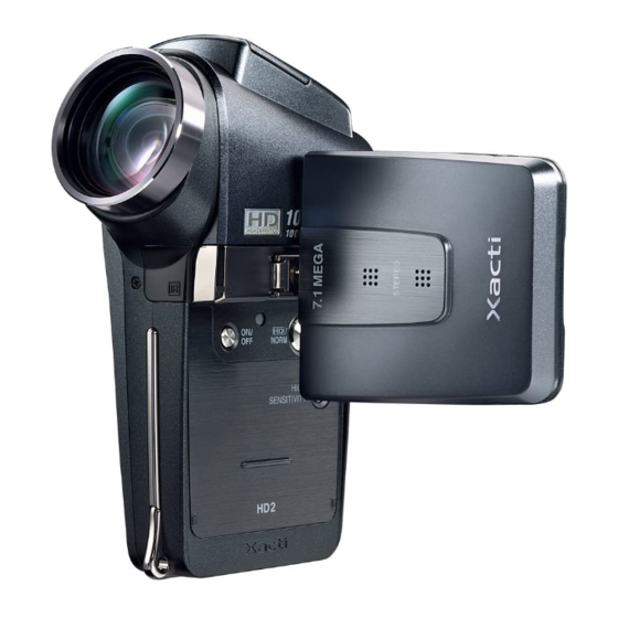
VPC-HD2
(Product Code : 168 091 01)
(U.S.A.) (Canada) (Korea)
(Taiwan) (General)
VPC-HD2EX
(Product Code : 168 091 02)
(Europe) (U.K.) (South America)
(China) (Australia) (Hong Kong)
(Russia) (Middle East)
(Africa) (General)
VPC-HD2GX
(Product Code : 168 091 03)
(South America) (China)
(Australia) (General)
(Korea) (Taiwan)
REFERENCE No. SM5310698
Advertisement
Chapters
Table of Contents

Related Manuals for Sanyo VPC-HD2


Summary of Contents for Sanyo VPC-HD2
-
Page 1: Table Of Contents
FILE NO. SERVICE MANUAL Digital Movie Camera VPC-HD2 (Product Code : 168 091 01) (U.S.A.) (Canada) (Korea) (Taiwan) (General) VPC-HD2EX (Product Code : 168 091 02) (Europe) (U.K.) (South America) (China) (Australia) (Hong Kong) (Russia) (Middle East) (Africa) (General) VPC-HD2GX Contents 1. - Page 2 WARNING Do not use solder containing lead. Note: This product has been manufactured using lead-free solder in If replacing existing solder containing lead with lead-free sol- order to help preserve the environment. der in the soldered parts of products that have been manufac- Because of this, be sure to use lead-free solder when carrying tured up until now, remove all of the existing solder at those out repair work, and never use solder containing lead.
-
Page 3: Outline Of Circuit Description
1. OUTLINE OF CIRCUIT DESCRIPTION Pin 1 1-1. CCD CIRCUIT DESCRIPTION 1. IC Configuration The CCD peripheral circuit block basically consists of the fol- lowing ICs. IC931 (MN39630PMJ-A) CCD imager IC901 (AN20113A) V driver IC905 (AD9971BCPZRL) CDS, AGC, A/D converter, H driver, vertical TG Pin 15 2. - Page 4 3. IC901 (V Driver) 4. IC905 (H Driver, CDS, AGC and A/D converter) A V driver (IC901) is necessary in order to generate the clocks IC905 contains the functions of H driver, CDS, AGC and A/D (vertical transfer clock and electronic shutter clock) which converter.
- Page 5 1-2. CP1 and VF1 CIRCUIT DESCRIPTION 1. Circuit Description 2. Outline of Operation 1-1. Digital clamp When the shutter opens, the reset signals (ASIC and CPU) The optical black section of the CCD extracts averaged values and the serial signals (“take a picture” commands) from the 8- from the subsequent data to make the black level of the CCD bit microprocessor are input and operation starts.
- Page 6 4. Lens drive block 5. Video Clip Recording and Playback 4-1. Focus drive 5-1. Recording The 16-bit serial data signals (LENS_SD) and (LENS_CK and The signal from the camera block is input to IC101 (ASIC). The LENS_EN) which are output from the ASIC (IC101) are used data that is input to the ASIC is input to SDRAM, and input to to drive (FOCUS A +, FOCUS A -, FOCUS B + and FOCUS B IC102 (MOVIC2) through D1 (I/F).
- Page 7 1-3. PW1 POWER CIRCUIT DESCRIPTION 1. Outline 3. Motor System Power Output This is the main power circuit, and is comprised of the follow- 5.3 V is output. Feedback for the 5.3 V is provided to the switch- ing blocks. ing controller (Pin (36) of IC501) so that PWM control can be Switching controller (IC501) carried out.
- Page 8 1-4. PW1 STROBE CIRCUIT DESCRIPTION 1. Charging Circuit 2. Light Emission Circuit When UNREG power is supplied to the charge circuit and the When FLCLT signal is input from the ASIC, the stroboscope CHG signal from microprocessor becomes High (3.3 V), the emits light.
- Page 9 1-5. SYA CIRCUIT DESCRIPTION 1. Configuration and Functions For the overall configuration of the SYA block, refer to the block diagram. The SYA block centers around a 8-bit microprocessor (IC301), and controls camera system condition (mode). The 8-bit microprocessor handles the following functions. 1.
- Page 10 BAT_TEMP Lithium battery temperature detection COMREQ Command request input Battery OFF detection signal input (L= OFF detection) BAT_OFF Serial communication request signal (interruption) SREQ SCAN IN6 Keyscan input 6 IR_IN Infrared remote control communication data input RESET Reset input power monitoring XCIN Clock (32.768 kHz) XCOUT...
- Page 11 4. Power Supply Control The 8-bit microprocessor controls the power supply for the overall system. The following is a description of how the power supply is turned on and off. When the battery is attached, a regulated 3.2 V voltage is normally input to the 8-bit microprocessor (IC301) by IC302, so that clock counting and key scanning is carried out even when the power switch is turned off, so that the camera can start up again.
-
Page 12: Disassembly
2. DISASSEMBLY 2-1. REMOVAL OF CABI LEFT, PW1 BOARD AND CP1 BOARD 1. Open the cover battery. 2. Screw 1.7 x 5 When assembling, 3. Screw 1.4 x 3 tighten the screws order. 4. Screw 1.7 x 4 a → b 5. - Page 13 2-2. REMOVAL OF LENS ASSEMBLY AND CA1 BOARD 1. Screw 1.7 x 3.5 2. Compl, cabi front 3. Assy lens 4. Screw 1.7 x 2 5. Screw 1.7 x 3.5 6. Earth plate back 7. Unit control 8. Three screws 1.7 x 2 9.
- Page 14 2-3. REMOVAL OF TB1 BOARD AND ST1 BOARD 1. Spacer tube 2. Screw 1.7 x 2.5 3. Two screw 1.7 x 3.5 4. Open the cover jack. 5. Two screws 1.7 x 3 6. Holder flash base 7. Unit sw FPC 8.
- Page 15 2-4. REMOVAL OF LCD, VF1 BOARD AND TB2 BOARD 1. Spacer joint When assembling, 2. Button power tighten the screws 3. Screw 1.7 x 2.5 order. 4. Spring button LCD A or B → C or D 5. Button LCD 6.
- Page 16 2-5. BOARD LOCATION VF1 board ST1 board TB1 board CA1 board PW1 board TB2 board CP1 board – 16 –...
-
Page 17: Electrical Adjustment
URL. place before using Color Pure. It is used after adjusting the chroma meter (VJ8-0192) adjust color temperature to 3100 ± http://www.digital-sanyo.com/overseas/service/ 20 K and luminosity to 900 ± 20 cd/m . Be careful of handling the lump and its circumference are high temperature during use and after power off for a while. - Page 18 3-6. The adjustment item which in necessary in part exchange CCD Black CCD White Point And Lens Point Factory White Point Language storage Reset Defect Adjust- Adjust- Cord Defect Detect Setting information Setting Detect Setting ment ment Adjustment registration Adjustment In Lighted COMPL PWB CP-1 COMPL PWB VF-1...
- Page 19 2. AWB Adjustment Adjustment value determination is effectuated using the "AGC", “monit_AGC”, “CHECK", “CHECK_ND”, “IRIS_GAIN”, “IRIS_OFFSET”, "MS" and “IRIS” values. If AGC= a1, a2, a3, a4, a5, a6, a7 monit_AGC= am1 CHECK= wc0, wc1, wc2 CHECK_ND= wnc0, wnc1, wnc2 IRIS_GAIN= g, IRIS_OFFSET= o, MS= ms1, ms2, ms3, ms4, ms5 IRIS= s1, s2, s3, s4, s5...
- Page 20 4. CCD Black Point And White Point Defect Detect 3-8. Factory Code Setting Adjustment In Lighted 1. Check the "Factory Code" display within the Setting group. 2. For U.S.A., Canada and NTSC general area If "FC_SANYO_U" does not appear, click on the " "...
- Page 21 3-12. Firmware uploading procedure 1. Uploading the firmware should be carried out if the version number (COMPL PWB XX-X) on the replacement circuit board is lower than the version of the distributed firmware. For XX-X, enter the name of the circuit board containing the firmware.
-
Page 22: Usb Storage Information Registration
17.) 2. Double-click on the DscCalDi.exe. 3. Click on the Get button in the USB storage window and check the USB storage data. VID: SANYO PID: HD2 Serial: Rev. : 1.00 4. -
Page 23: Troubleshooting Guide
5. TROUBLESHOOTING GUIDE POWER LOSS INOPERTIVE TAKING INOPERATIVE PUSH SHUTTER PUSH THE POWER BUTTON SW FOR A WHILE IC301-32, 31 IC301-44 CHECK S3103 (SCAN IN 3, 4) CHECK D3004 (SCAN OUT2) PULSE INPUT PULSE INPUT CL527 (PON2) CHECK IC301, IC101, IC303-7 5.3 V CL519 (PON) CHECK IC501... -
Page 24: Parts List
CARTON INNER-SG113/EX Note: Refer to the table of accessories. VPC-HD2EX, VPC-HD2GX 645 091 8612 ADAPTOR,DOCKING STATION(SVS01/WA) 7002 636 101 6896 CARTON INNER-SG113/U, VPC-HD2 ONLY 645 080 4434 CABLE,DSC A/V-SX812 7003 636 077 8139 CUSHION SHEET-SX774/KRO (Dedicated SAV interface cable) 7004... - Page 25 1.Table of accessories...
- Page 26 CABINET AND CHASSIS PARTS 1 LOCATION PARTS NO. DESCRIPTION LOCATION PARTS NO. DESCRIPTION 636 101 6582 BUTTON COVER BATT-SG113/J 636 102 4914 DEC FRONT-SG113/J 636 101 6599 COVER BATTERY-SG113/J 636 094 0710 HEAT SINK RUBBER A-SX812 636 091 6357 SPACER BATTERY-SX812/J 645 079 5701 SPEAKER,8 636 096 0749...
- Page 27 CABINET AND CHASSIS PARTS 1 N.S.P. N.S.P.: Not available as service parts. Cabinet 1 SG113/J PARTS LIST 1...
- Page 28 CABINET AND CHASSIS PARTS 2 LOCATION PARTS NO. DESCRIPTION LOCATION PARTS NO. DESCRIPTION 636 101 6711 DEC RIGHT-SG113/J 636 090 7911 ADHESIVE DEC LCD-812 636 090 8079 SPACER LENS RIGHT-SX812/J 636 095 0696 SPACER COVER LCD-SX812/J 636 089 4358 REFLECTOR LED-SX812/J 636 097 3985 DEC LCD TOP-SX819/J 636 090 7942...
- Page 29 CABINET AND CHASSIS PARTS 2 Cabinet 2 SG113/J PARTS LIST 2...
- Page 30 ELECTRICAL PARTS Note: 1. Materials of Capacitors and Resistors are abbreviated as follows ; Resistors Capacitors MT-FILM Metallized Film Resistor MT-POLYEST Metallized Polyester Capacitor MT-GLAZE Metallized Glaze Resistor MT-COMPO Metallized Composite Capacitor OXIDE-MT Oxide Metallized Film Resistor TA-SOLID Tantalum Solid Capacitor AL-SOLID Aluminum Solid Capacitor NP-ELECT...
- Page 31 LOCATION PARTS NO. DESCRIPTION LOCATION PARTS NO. DESCRIPTION L1012 645 053 2702 IMPEDANCE,22 OHM P C1301 303 381 8109 CERAMIC 1U K 6.3V L1013 645 053 2702 IMPEDANCE,22 OHM P C1401 303 338 0309 CERAMIC 0.1U K 10V L1061 645 059 7596 IMPEDANCE,90 OHM P C1403 303 309 2509...
- Page 32 LOCATION PARTS NO. DESCRIPTION LOCATION PARTS NO. DESCRIPTION C9065 303 155 1800 CERAMIC 0.01U K 25V R1019 301 225 7905 MT-GLAZE 220 JA 1/16W C9066 303 276 1307 CERAMIC 1000P K 50V R1020 301 225 0302 MT-GLAZE 33 JA 1/16W C9067 303 276 1307 CERAMIC...
- Page 33 LOCATION PARTS NO. DESCRIPTION LOCATION PARTS NO. DESCRIPTION R1304 301 226 1506 MT-GLAZE 0.000 ZA 1/16W R9721 301 262 1904 MT-GLAZE 6.8K DC 1/16W R1321 301 226 1506 MT-GLAZE 0.000 ZA 1/16W R9722 301 262 1607 MT-GLAZE 2.2K DC 1/16W R1322 301 226 1506 MT-GLAZE 0.000 ZA 1/16W...
- Page 34 LOCATION PARTS NO. DESCRIPTION LOCATION PARTS NO. DESCRIPTION IC503 309 657 0105 IC TK11112CSC-G (RESISTOR PACK) IC504 409 680 8205 IC XC9215C18CD RB541 645 078 5702 R-NETWORK 1KX2 0.063W IC521 309 652 1909 IC LTC4061EDD-4.4PBF (RESISTORS) IC541 309 671 6602 IC TPS65560RGT R5002 301 258 7101...
- Page 35 LOCATION PARTS NO. DESCRIPTION LOCATION PARTS NO. DESCRIPTION COMPL PWB,TB-2 COMPL PWB,ST-1 636 100 7764 636 100 7740 (SWITCH) (TRANSFORMER) S6501 645 051 5385 SWITCH,PUSH 1P-1TX1, T5402 645 068 1721 TRANS,STEP UP (MISCELLANEOUS) 636 099 4058 ASSY,WIRE VF1&TB2-SX819 COMPL PWB,VF-1 636 100 7726 (SEMICONDUCTOR) Q1702...
-
Page 36: Circuit Diagrams & Printed Wiring Boards
CIRCUIT DIAGRAMS & PRINTED WIRING BOARDS TABLE OF CONTENTS OVERALL WIRING & BLOCK DIAGRAMS Page OVERALL WIRING ............................C3 OVERALL CIRCUIT ............................C4 POWER CIRCUIT ............................. C4 CCD CIRCUIT ..............................C5 LENS CIRCUIT ..............................C5 MAIN CIRCUIT ..............................C6 SYSTEM CONTROL CIRCUIT ........................C7 STROBE CIRCUIT ............................ - Page 37 NOTES: 1. All resistance values in "OHMS" unless otherwise noted. (K=1,000 ; M=1,000,000) µ 2. All capacitance values in " F" unless otherwise noted. µ p=pico farad ; ,u or U=micro farad µ 3. All inductance values in " H" unless otherwise noted. µ...
-
Page 38: Overall Wiring & Block Diagrams
OVERALL WIRING & BLOCK DIAGRAMS OVERALL WIRING LENS SW UNIT BATTERY CN103 CN502 BATCHGI BATCHGI +12V(A) +12V(A) LCD AN POWER POWER_IN JW173 POWER POWER_IN LCD CA JW174 POWER POWER_IN POWER POWER_IN CN170 CN106 POWER POWER_IN VCOM VDD3 VDD3 POWER POWER_IN TEST +12V(L) +12V(L) -
Page 39: Overall Circuit
OVERALL CIRCUIT POWER CIRCUIT POWER_IN IC521 CHG_CNT CA1 BOARD TO CP1 (DMA) CP1 BOARD CHRG CAMERA BLOCK LTC4061EDD BATCHGER BATTERY BATTERY TO BATTERY PROG IC901 CHARGE BATCHGI V. DRIVER SW Q5006 IC931 1/2.5" IC102 +12V(L) AUDIO BLOCK 7.3M IC905 MOVIC SW Q5007 L5005,Q5003 IC503... -
Page 40: Ccd Circuit
CCD CIRCUIT LENS CIRCUIT IC951 BU2233GU LENS DRIVER CN951 J4,J8 +12V(A) -6V(A) LENS_BLOCK B7,A2 BOOST5.3V MVCC12,MVCC34 IC101 ASIC ZOOM VCC LENS O_LPF VDD3 MVCC56,VDDAMP EV1MSS Q9301 ZOOM_PI 25 CCDINP TCLKP AFECKP VDD3 DVDD Vout IC905 TCLKN AFECKN ZPIOUT Z_SENSE AD9971BCPZRL DOUT0P AFESD1P IC931... -
Page 41: Main Circuit
MAIN CIRCUIT CA1 BOARD CN902-CN931 IC904 NJM2877F3 DATA VDD3 IC103 REG 3.0V ADDRESS K4M56323PG +3.4V(A) ZRAS,ZCAS -6V(A) 256M SDRAM +12V(A) ADCK IC905 SERIAL IC199 H.DRIVER 5, 6 AFECKP/N U1, U2 27MHz AD9971BCPZRL CDS, AGC, 7, 8 AFESD1P/N V1, V2 CCD OUT AK8113L A/D C, 3, 4... -
Page 42: System Control Circuit
SYSTEM CONTROL CIRCUIT STROBE CIRCUIT AL3.2V BOOST5.3V CHARGING CIRCUIT C5401 T5401 D5402 BACKUP3.2V TO TCA LENS_4M POWER FILTER OSCILLATION RECTIFIER LENS_4M IC302 C5412 BOOST5.3V VDD2 BLOCK TRANSFORMER CIRCUIT BATTERY LCDON1 TO DMA VDD3 LCD ON BACKUP PON2 VDD1 P ON2 BD4289FVM P ON RESET... -
Page 43: Circuit Diagrams
CIRCUIT DIAGRAMS PW1 BOARD POWER & STROBE ST1 BOARD TRIGGER TRANS 2A32V STROBE UNIT F5001 T5402 JW553 AWG30 TTR-1026R-01 JW551 AWG28 DCIN SI3473DV 1608 TRGOUT TRGIN Q5201 L5003 D5006 T5401 BLUE WHITE FBMH1608HL300 RB060M-30 2.0X1.25 2.2X1.5 1AV4L17B0480G POWER_IN D5402 TTRN-0530-008-T TO STROBE UNIT JW541 AWG26... -
Page 44: Ca1 Board Ccd
CA1 BOARD CCD CN931 R9302 430;1/16J 1AV4J11SE341G SUBGT VSUB R9301 47;1/16J Q9301 UP05C8G -6V(A) +12V(A) +12V(A) CCDOUT CCDOUT TO CP1(CAA) C1-09100/SG113-J CN902 VOLTAGE: VIEW MODE, LCD ON... -
Page 45: Cp1 Board (Caa) Ccd Afe & Driver
CP1 BOARD (CAA) CCD AFE & DRIVER Q9001 SSM3J16TE PAON2 C9029 1;B 16 1608 C9030 CN902 1608 R9015 0;1/16Z -6V(A) -6V(A) C9040 1AV4J10LM341G +12V(A) +12V(A) SUBGT SUBGT +3.4V(A) +3.4V(A) TO DMA C9076 0.1;B VDD3 VDD3 V. DRIVER VSUB PAON3 PAON3 SUBCNT SUBCNT CCD_RG... -
Page 46: Cp1 Board (Dma) Main
CP1 BOARD (DMA) MAIN CN103 1AV4J10JL600G BATCHGI BATCHGI M_VDD1.8 M_VDD3 M_VDD1.2 VA104 VA105 VA106 +12V(A) +12V(A) AVR-M1005C080MTAAB AVR-M1005C080MTAAB AVR-M1005C080MTAAB POWERIN POWER C1006 C1071 DMA (MAIN) C1007 0.1;B POWER 0.1;B 0.1;B C1012 C1013 0.1;B 0.1;B C1072 POWER C1008 0.1;B 0.1;B POWER C1014 C1073 D1-09100/SG113-J... - Page 47 CP1 BOARD (DMA) MAIN [UPPER-LEFT] R1078 10K;1/16J R1152 10K;1/16J 10K;1/16J R1080 1608 L1009 FBMH1608HM102 VDD3 VDD1.2 L1010 FBMH1608HM601 1608 SA12 SA12 SA13 SA13 SA14 SA14 ZRWE ZRWE ZCAS ZCAS ZRAS CLOCK GEN. ZRAS ZRCE ZRCE GEN_OE R1009 CKRE CLKOUT R1065 CKRE 33;1/16J FSEL...
- Page 48 CP1 BOARD (DMA) MAIN [UPPER-RIGHT] CN103 1AV4J10JL600G BATCHGI BATCHGI M_VDD1.8 M_VDD3 M_VDD1.2 VA104 VA105 VA106 +12V(A) +12V(A) AVR-M1005C080MTAAB AVR-M1005C080MTAAB POWER AVR-M1005C080MTAAB POWERIN DMA (MAIN) C1006 C1071 0.1;B 0.1;B C1007 C1012 POWER 0.1;B C1013 0.1;B 0.1;B C1072 POWER 0.1;B C1008 0.1;B POWER D1-09100/SG113-J C1014...
- Page 49 CP1 BOARD (DMA) MAIN [LOWER-LEFT] VSSQ1 COMPAO SDD13 R1056 GPIOC22 VREFAO ZSCAS 750;1/16D COMREQ GPIOC18 AOUT AB12 ZPIOUT SYSTEM ASIC GPIOC17 AVDD33D_ADAC SDA3 FPIOUT GPIOC16 AVSS33D_ADAC SDA7 C1052 VDD1 AVDD33AR_VDAC SDA13 0.1;B VSS1 COMPV AA12 FILTER_SEL GPIOC7 VREFV VSSQ R1053 R1058 I2C_SCLK GPIOC6...
- Page 50 CP1 BOARD (DMA) MAIN [LOWER-RIGHT] COMPAO SDD13 XSG2C LCDD7 LCDD6 R1082 120;1/16J R1056 LCDD6 VREFAO ZSCAS XSG3A 750;1/16D R1083 120;1/16J VDATA2 LCDD5 AOUT AB12 D1D2 LCDD5 LCDD4 R1084 120;1/16J LCDD4 AVDD33D_ADAC SDA3 CCDOD8 R1085 120;1/16J LCDD3 AVSS33D_ADAC SDA7 IO_POWER_3_COMMON LCDD3 VSYNC LCDD2 R1086...
- Page 51 LCD DRIVER CIRCUIT WAVEFORMS MAIN CIRCUIT WAVEFORMS TEST POINT TEST POINT TEST POINT TEST POINT WAVEFORM WAVEFORM WAVEFORM WAVEFORM LOCATION LOCATION LOCATION LOCATION IC101 IC102 CN177 CN177 PIN A11 PIN AB18 PIN 21 PIN 15 MVINCLK XOUT 1V/div 1V/div 1V/div 1V/div 4ns/div 10ns/div...
-
Page 52: Cp1 Board (Tca) Lens
CP1 BOARD (TCA) LENS +3.4V(A) +3.4V(A) VDD3 VDD3 BOOST5.3V TO DMA R9508 0;1/16Z IC551 H=1.55 VDD3 REG. XC9215C40CD-R CN951 1608 QXC9215C40CDP L5501 IC552 4.7;N XC6204B342DR 1AV4J11VE250G 3.0X3.0 FOCUS_B- FOCUS B- 1AV4L2NK4R7NG PAON3 VOUT FOCUS_A- FOCUS A- CE/MODE FOCUS_B+ FOCUS B+ FOCUS_A+ VOUT FOCUS A+... -
Page 53: Cp1 Board (Sya) System Control
CP1 BOARD (SYA) SYSTEM CONTROL AL3.2V AL3.2V SW3.2V BOOST5.3V BOOST5.3V UNREG_SY UNREG_SY IR_IN ZSREQ COMREQ R3024 Y1-09100/SG113-U BAT_T 47K;1/16J ZAVJACK VOLTAGE: VIEW MODE, LCD ON BATCHGI UV0_ZBOOT R3019 Q3004 PDTC123EE 47K;1/16J DCIN TO DMA SI2C SI2C HD/SD SI2D SI2D S3002 C3016 1000P;B LS15D2... -
Page 54: Tb1 Board Mic Jack
TB1 BOARD MIC JACK VF1 BOARD LCD DRIVER & MIC AMP TO CP1 (DMA) CN106 TO CP1 (DMA) S3103 VDD3 CN181 ESE13V01C CN170 JW173 CN651 TO LCD JK651 1AV4J10UC203G AWG26/24 LGK1709-1601 1AV4J11VA062G 1AV4J12B3140G VDD3 LCD AN POPUP_SW POPUP_SW R3101 0;1/16Z +12V(L) JW174 VCOM... -
Page 55: Printed Wiring Boards (P.w.b.)
PRINTED WIRING BOARDS (P.W.B.) CP1 P.W.B. (SIDE A) -
Page 56: Cp1 P.w.b. (Side B)
CP1 P.W.B. (SIDE B) -
Page 57: Pw1 P.w.b. (Side A)
PW1 P.W.B. (SIDE A) -
Page 58: Pw1 P.w.b. (Side B)
PW1 P.W.B. (SIDE B) -
Page 59: Ca1 P.w.b. (Side A & B)
CA1 P.W.B. (SIDE A) CA1 P.W.B. (SIDE B) IC931... -
Page 60: Tb1 P.w.b. (Side A & B)
TB1 P.W.B. (SIDE A) TB1 P.W.B. (SIDE B) ST1 P.W.B. (SIDE A) ST1 P.W.B. (SIDE B) SIDE-A TB2 P.W.B. (SIDE A) TB2 P.W.B. (SIDE B) SIDE-A S6501 There is neither the pattern nor the part on B side. -
Page 61: Vf1 P.w.b. (Side A &B)
VF1 P.W.B. (SIDE A) VF1 P.W.B. (SIDE B) - Page 62 SANYO Electric Co., Ltd. Osaka, Japan Printed in Japan Feb./’07...