Table of Contents
Advertisement
Advertisement
Table of Contents

Related Manuals for MiTAC PH10LU


Summary of Contents for MiTAC PH10LU
- Page 1 MITAC Desktop Board PH10LU Product Guide...
-
Page 2: Desktop Board Features
Desktop Board Features This chapter briefly describes the features of Desktop Board PH10LU. Table 1 summarizes the major features of the Desktop Board. Feature Summary 1. M TAC D PH10LU F ABLE ESKTOP OARD EATURES Form Factor Micro-ATX (244 millimeters [9.6 inches] x 244 millimeters [9.6... - Page 3 PCI Express* Full-Mini Card slot with Half-Mini Either Option Card support Peripheral USB 3.0 back panel connectors (blue) Interfaces USB 2.0 back panel connectors (black) USB 3.0 front panel ports 2 (Headers) USB 2.0 front panel ports 4 (Headers) Serial ATA (SATA) 6.0 Gb/s interfaces Hardware Monitor Hardware monitoring through the Nuvoton* NCT6104D legacy Subsystem...
-
Page 4: Desktop Board Components
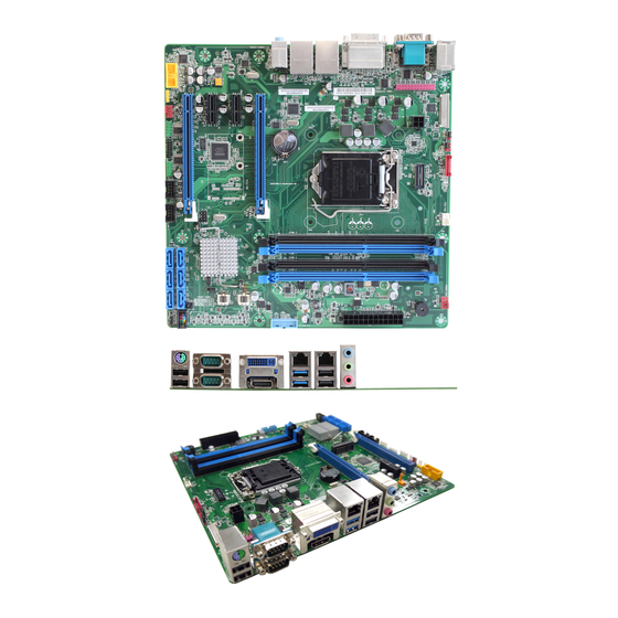
Desktop Board Components Figure 1 shows the approximate location of the major components on the top side of MiTAC Desktop Board PH10LU. Figure 1. MiTAC Desktop Board PH10LU Components (Top) - Page 5 2. M TAC D PH10LU C ABLE ESKTOP OARD OMPONENTS HOWN IN IGURE Back Panel Connectors Parallel Port Header LVDS Connector (Optional) 4-pin Power header LVDS power 1x3 pin header (Optional) LVDS power header (3V, 5V, 12V) (Optional) LVDS inverter board header (Optional)
-
Page 6: System Memory
Processor The board supports 4th generation Intel Core processors. Other processors may be supported in the future. This board supports processors with a maximum wattage of 95 W Thermal Design Power (TDP). NOTE This board has specific requirements for providing power to the processor. Additional power required will depend on configurations chosen by the integrator. -
Page 7: Connecting To The Internal Headers And Connectors
Connecting to the Internal Headers and Connectors Front panel main header Figure 2 Front panel main header pin-out Signal Name Description Signal Name Description Pull-up resistor (750 ) to +5V HDD_POWER_LED POWER_LED_MAIN [Out] Front panel LED (main color) HDD_LED# [Out] Hard disk activity LED POWER_LED_ALT [Out] Front panel LED (alt color) GROUND... - Page 8 Chassis Intrusion Detection Header The chassis intrusion detection header must be 1x2, 2.54mm pitch, colored black and with extended back, as defined in below Figure 3 Chassis intrusion detection header Signal Name Intrusion Detection Ground ABLE HASSIS INTRUSION DETECTION HEADER SIGNALS HD Audio front panel audio header Figure 4 HD Audio front panel audio header pin-out diagram...
- Page 9 Signal name Description Analog Port 1 - Left channel (Microphone) 1 PORT 1L Ground 2 GND Analog Port 1 - Right channel (Microphone) 3 PORT 1R Active low signal that signals BIOS that an Intel® HD Audio dongle is connected to the analog header.
-
Page 10: Internal Spdif Header
Internal SPDIF header Figure 5 Internal SPDIF header pin-out diagram Signal name Description Ground SPDIF_OUT SPDIF signal from the codec Key (no pin) Key (no pin) +5V_DC 5V power (for optical/TOSLINK module) SPDIF ABLE NTERNAL HEADER Front panel USB header Figure 6 Front panel USB header pin-out Signal Signal... -
Page 11: Parallel Port Header
Parallel port header Figure 7 Parallel port header pin-out Standard Signal Name ECP Signal Name EPP Signal Name STROBE# STROBE# WRITE# AUTOFD# AUTOFD#, HOSACK DATASTB# FAULT# FAULT#, PERIPHREQST# FAULT# INT# INT#, REVERSERQST# RESET# SLCTIN# SLCTIN# ADDRSTB# GROUND GROUND GROUND GROUND GROUND GROUND GROUND... -
Page 12: Serial Port Header
Serial port header Figure 8 Serial port header pin-out Signal Signal DCD (Data Carrier Detect) RXD# (Receive Data) TXD# (Transmit Data) DTR (Data Terminal Ready) Ground DSR (Data Set Ready) RTS (Request To Send) CTS (Clear To Send) RI (Ring Indicator) Key (no pin) ABLE ERIAL PORT HEADER SIGNALS... -
Page 13: Processor Fan Header
IntA_P1_D+ USB3 ICC Port1 D- (USB2 Signal D+) Over Current Protection IntA_P2_D+ USB3 ICC Port2 D+ (USB2 Signal D+) IntA_P2_D- USB3 ICC Port2 D- (USB2 Signal D-) Ground Ground IntA_P2_SSTX+ USB3 ICC Port2 SuperSpeed Tx+ IntA_P2_SSTX- USB3 ICC Port2 SuperSpeed Tx- Ground Ground IntA_P2_SSRX+... - Page 14 Front/Rear fan header Figure 11: Front/Rear fan header Signal FAN_CTRL FAN_TACH VCC-12V 11: P ABLE ROCESSOR FAN HEADER LVDS panel voltage selection header Pins 2&4: jumper position for 3.3V Pins 6&4: jumper position for 5V Pins 3&4: jumper position for 12V Figure 12: LVDS panel voltage selection header...
- Page 15 Signal Name VCC3/3V LCD SEL PWR VCC/5V 12: LVDS ABLE PANEL VOLTAGE SELECTION HEADER Inverter power voltage selection header Pins 1&2: jumper position for 5V Pins 3&2: jumper position for 12V Figure 13: Inverter power voltage selection header Signal Name 1 VCC/5V 2 BKLT_PWR 3 12V...
- Page 16 LVDS Pin Signal Name Description 1 BKLT_EN Backlight enable 2 BKLT_PWM Backlight PWM control 3 5V/12V Inverter power 4 5V/12V Inverter power 5 GND Ground 6 GND Ground 7 BRIGHTNESS_UP BRIGHTNESS UP 8 BRIGHTNESS_DOWN BRIGHTNESS DOWN 14: 8- LVDS ABLE INVERTER POWER HEADER PIN OUT REFERENCE Pin Signal...
-
Page 17: Alternate Power Led Header
27 LA_CLKN LVDS Channel A diff data output - negative 28 GND Ground 29 GND Ground 30 GND Ground 31 EDID_CLK EDID/DDC clock signal 32 BKLT_EN 33 BKLT_CTRL 34 LB_CLKP LVDS Channel B diff data output - positive 35 LB_CLKN LVDS Channel B diff data output - negative 36 BKLT_PWR Selectable BKLT power output... -
Page 18: Cmos Clear
RJ45 LED Behavior Diagram Color State Condition LAN link is not established Link LAN link is established Green Blinking LAN activity occurring 10 Mb/s data rate Green 100 Mb/s data rate Speed Yellow 1000 Mb/s data rate 17: RJ45 LED ABLE BEHAVIOR Note: LAN solution must be tested for IEEE802.3 conformance. - Page 19 MITAC Desktop Board PH10LU BIOS Specifiction...
-
Page 20: General Overview
GENERAL OVERVIEW This document specifies the BIOS requirements for PH10LU Note: The BIOS specification may be changed depend on hardware design. This is based on the product specification document (PRD). HARDWARE OVERVIEW - Intel Haswell Series. - Socket Type: LGA1150... - Page 21 Chassis Intrusion Header x1 Audio Header (Front Panel Mic / Hp) S/PDIF Out Audio Header 4-pin CPU Fan Header 4-pin Front Fan Header 4-pin Rear Fan Header External I/O USB 2.0 x4 USB 3.0 x2 PS2 x1 Serial Port x2 RJ45 x1 3-stack Audio Jack Supporting OS...
-
Page 22: Bios Overview
Management Engine Specification : 493796_493796_Revision_1p2_ME9_0_5MB.pdf Super I/O Specification : NCT6104D_Datasheet_v1_5.pdf Others : 368119_Intel®_Graphics_Media_Accelerator–Binary_Modification_Program_User’s_Guide_Rev2_5.pdf Intel High Definition Audio (Programmers Reference Manual).pdf 503098_UEFI_Graphics_Output_Protocol_Driver_BIOS_Integration_Guide_Rev_1_0.pdf BIOS OVERVIEW AMI APTIO 4.6.5.3 BIOS, UEFI Version = 2.3.1 , PI Version = 1.2 Code Base : 1AQQW026 Support Platform : Intel Shark-Bay Support IGD VBIOS : 2171 / Intel GOP VBIOS : 165 Provide BIOS Setup Utility... - Page 23 initialized, control is transferred to the INT 19h Bootstrap Loader, to load the available operating system on the disk. During the POST period, a value form 00h through FFh is written to the manufacturing test port (generally is I/O port 80h). These values are known as POST Diagnostic Codes.
- Page 24 The Subsystem Vendor ID is that of the board/card manufacturer. The Subsystem Device ID is assigned by the subsystem vendor. For on-brand board/system, BIOS needs to configure MiTAC SVID as manufacturer ID (to identify for DTM verification) & SSID (used project code).
- Page 25 MXIC MX25L3273 BIOS RELEASE BIOS REVISION D727 0 A 01 MiTAC BIOS Naming: SKU B/C 1 1: Sku ID; “0” for MiTAC 2: Stage; =>Develop Stage. =>Test Stage. A =>Production Stage 3: Version number (Decimal); RELEASE COMPONENT Release BIOS ROM and Flash Utility for each BIOS release. If Flash Utility is not modified, may not...
- Page 26 Send Release Note for each BIOS release. Release Note contains added features, fixed issues & known restriction. BIOS RELEASE FTP Server EMAIL DISTRIBUTION LIST FOR BIOS RELEASE Customer, RD, CAD, QA. BIOS RELEASE NOTE FORMAT //******************************************************************************** // Revision No. // Build Date // ME Version // GbE PHY // GbE Option Rom Version :...
-
Page 27: Maintenance
MAINTENANCE Support new function and new OS in nearly future as many as possible Support simple changing from our customer’s BIOS requests. For example, - Change the default value in BIOS Setup - Change the boot device order in BIOS Setup. BIOS QA TEST Must to PASS below tests before release BIOS version (correct version) - Page 28 AP initialization before microcode loading North Bridge initialization before microcode loading South Bridge initialization before microcode loading OEM initialization before microcode loading Microcode loading AP initialization after microcode loading North Bridge initialization after microcode loading South Bridge initialization after microcode loading OEM initialization after microcode loading Cache initialization SEC Error Codes...
- Page 29 0x36 CPU post-memory initialization. System Management Mode (SMM) initialization 0x37 Post-Memory North Bridge initialization is started 0x38 Post-Memory North Bridge initialization (North Bridge module specific) 0x39 Post-Memory North Bridge initialization (North Bridge module specific) 0x3A Post-Memory North Bridge initialization (North Bridge module specific) 0x3B Post-Memory South Bridge initialization is started 0x3C...
- Page 30 Recovery Error Codes 0xF8 Recovery PPI is not available 0xF9 Recovery capsule is not found 0xFA Invalid recovery capsule 0xFB – 0xFF Reserved for future AMI error codes PEI Beep Codes Status Code Description 0x53 Three long beep - Memory initialization error. No usable memory detected DXE Status Codes Status Code Description...
- Page 31 0x96 PCI Bus Assign Resources 0x97 Console Output devices connect 0x98 Console input devices connect 0x99 Super IO Initialization 0x9A USB initialization is started 0x9B USB Reset 0x9C USB Detect 0x9D USB Enable 0x9E – 0x9F Reserved for future AMI codes 0xA0 IDE initialization is started 0xA1...
- Page 32 0xD8 Invalid password 0xD9 Error loading Boot Option (LoadImage returned error) 0xDA Boot Option is failed (StartImage returned error) 0xDB Flash update is failed 0xDC Reset protocol is not available DXE Beep Codes None ASL Status Codes Status Code Description 0x01 System is entering S1 sleep state 0x02...
-
Page 33: Battery Caution
A suitable caution label is included with MiTAC Desktop Board PH10LU. CAUTION Risk of explosion if the battery is replaced with an incorrect type. Batteries should be recycled where possible.
Need help?
Do you have a question about the PH10LU and is the answer not in the manual?
Questions and answers