Table of Contents
Advertisement
SERVICE MANUAL
Ver 1.0 2003.05
US and foreign patents licensed from Dolby
Laboratories.
CD player section
System
Compact Disc digital
audio system
Laser
Semiconductor laser
(λ=780 nm)
Frequency response
20 Hz – 20 kHz (±0.5 dB)
Wow and flutter
Below measureable limit
(±0.001% W.PEAK)
MD deck section
System
MiniDisc digital audio system
Disc
MiniDisc
Laser
Semiconductor laser
(λ=780 nm)
Emission duration:
continuous
Sampling frequency
44.1 kHz
Frequency response
20 Hz – 20 kHz (±0.5 dB)
Inputs
Jack type Input
Rated
impedance
input
ANALOG IN Pin jack
47 kilohms
500 mVrms
DIGITAL
Squqre
Optical wave
OPTICAL IN
optical
length:
–
connector
660 nm
jack
Sony Corporation
9-877-241-01
2003E05-1
Home Audio Company
C 2003.5
Published by Sony Engineering Corporation
MD
Section
CD
Section
SPECIFICATIONS
Minimum
input
250 mVrms
–
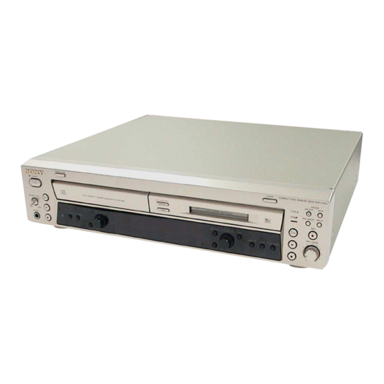
MXD-D400
Model Name Using Similar Mechanism NEW
MD Mechanism Type
Optical Pick-up Name
Model Name Using Similar Mechanism NEW
CD Mechanism Type
Base Unit Name
Optical Pick-up Name
Outputs
Jack type
Rated output
ANALOG OUT Pin jack
2 Vrms
(at 47 kilohms)
DIGITAL
Squqre optical
-18 dBm
OPTICAL OUT
connector jack
PHONES
Stereo phone
10 mW
jack
General
Power requirements
120 V AC, 60 Hz
Power consumption
19 watts
Less than 1 watt (at the
power saving mode)
Dimensions (w/h/d) incl. projecting parts and controls
Approx. 430 × 108 × 399 mm
Mass
Approx. 5.4 kg
Supplied accessories
• Audio connection cords (2)
• Remote commander (remote) (1)
• Sony R6 (size-AA) batteries (2)
Design and specifications are subject to change
without notice.
COMPACT DISC MINIDISC DECK
US Model
MDM-7S2C
KMS-262E
CDM66C-30B61M
BU-30BD61B
OP Assy (A-MAX.4T)
Load
impedance
Over 10 kilohms
Optical wave
length:660 nm
32 ohm
Advertisement
Table of Contents

Related Manuals for Sony MXD-D400


Summary of Contents for Sony MXD-D400
- Page 1 • Audio connection cords (2) Jack type Input Rated Minimum • Remote commander (remote) (1) impedance input input • Sony R6 (size-AA) batteries (2) ANALOG IN Pin jack 47 kilohms 500 mVrms 250 mVrms DIGITAL Squqre Optical wave Design and specifications are subject to change...
-
Page 2: Self-Diagnosis Function
To solve the problem refer to cErase all the recorded contents of the MD using the following list. If any problem persists, the All Erase Function. consult your nearest Sony dealer. C41/Cannot Copy The digitally dubbed material cannot be recorded digitally. - Page 3 MXD-D400 ITEMS OF ERROR HISTORY MODE ITEMS AND CONTENTS Selecting the Test Mode Display Details of History op rec tm Cumulative recording time is displayed. When cumulative recording time is over 1 minute, the hour and minute are displayed as they are.
- Page 4 MXD-D400 Table of Error Codes Error Code Details of Error Loading failed Loading switch combination is illegal Head of PTOC could not be read within the specified time Head of PTOC could be read but its content is erroneous Access to UTOC could not be made within the...
-
Page 5: Table Of Contents
MXD-D400 TABLE OF CONTENTS SELF-DIAGNOSIS FUNCTION 7-7. Base Unit Section (BU-30BD61M) ........ 89 ......2 ELECTRICAL PARTS LIST ....... 90 SERVICING NOTES ..........7 GENERAL ..............16 DISASSEMBLY 3-1. Disassembly Flow ............17 3-2. Case (409538) ..............18 3-3. Loading Panel (CD) ............18 3-4. - Page 6 LINE WITH MARK 0 ON THE SCHEMATIC DIAGRAMS AND IN THE PARTS LIST ARE CRITICAL TO SAFE OPERATION. REPLACE THESE COMPONENTS WITH SONY PARTS WHOSE PART NUMBERS APPEAR AS SHOWN IN THIS MANUAL OR IN SUPPLEMENTS PUB- LISHED BY SONY.
-
Page 7: Servicing Notes
MXD-D400 SECTION 1 SERVICING NOTES CLEANING OBJECTIVE LENS OF OPTICAL PICK-UP NOTES ON HANDLING THE OPTICAL PICK-UP • In cleaning the objective lens of optical pick-up, be sure the BLOCK OR BASE UNIT following below. The laser diode in the optical pick-up block may suffer electro- static break-down because of the potential difference generated 1. - Page 8 MXD-D400 SERVICE POSITION – Main board – main board – Front panel block section – front panel block section...
- Page 9 MXD-D400 – MD mechanism deck – BD (MD) board MD mechanism deck (MDM-7S2C) – CD mechanism deck – CD mechanism deck (CDM66C-30B61M)
- Page 10 MXD-D400 NOTE FOR POSITION OF THE CABLE (4P) Fix the cable (4P) between the transformer board and the main board with a lead pin keeping the cable from the powertransformer (TR651). power transformer (TR651) transformer board cable (4P) lead pin...
- Page 11 MXD-D400 MD SECTION JIG FOR CHECKING BD (MD) BOARD WAVEFORM The special jig (J-2501-196-A) is useful for checking the waveform of the BD (MD) board. The names of terminals and the checking items to be performed are shown as follows.
- Page 12 MXD-D400 IOP DATA RECORDING AND DISPLAY WHEN OPTICAL PICK-UP AND NON-VOLATILE MEMORY (IC195 OF BD (MD) BOARD) ARE REPLACED The IOP value labeled on the optical pick-up can be recorded in the non-volatile memory. By recording the value, it will eliminate the need to look at the value on the optical pick-up label.
- Page 13 MXD-D400 CHECKS PRIOR TO PARTS REPLACEMENT AND ADJUSTMENTS IN MD Before performing repairs, perform the following checks to determine the faulty locations up to a certain extent. Details of the procedures are described in “5 Electrical Adjustments”. Criteria for Determination...
- Page 14 MXD-D400 CD SECTION CD-TEXT TEST DISC This unit is able to display the test data (character information) written in the CD on its fluorescent indicator tube. The CD-TEXT TEST DISC (TGCS-313:4-989-366-01) is used for checking the display. To check, perform the following procedure.
- Page 15 MXD-D400 Table 2: CD-TEXT TEST DISC Recorded Contents and Display (In this unit, some special characters cannot be displayed. This is not a fault) TRACK Recorded contents Display ! ” # $ % & ´ (21h to 27h)1kHz 0dB L&R...
-
Page 16: General
MXD-D400 SECTION 2 This section is extracted from instruction manual. GENERAL Main unit Remote control 90qa ALPHABETICAL ORDER A – I ALBUM wh AMS wa wg CD SYNCHRO NORMAL/HIGH 4 CLEAR ws Disc tray 3 DISPLAY ql Display window wf... -
Page 17: Disassembly
MXD-D400 SECTION 3 DISASSEMBLY • This set can be disassembled in the order shown below. 3-1. DISASSEMBLY FLOW 3-2. CASE (409538) (Page 18) 3-3. LOADING PANEL (CD) 3-6. TRANSFORMER BOARD 3-7. MAIN BOARD (Page 18) (Page 20) (Page 20) 3-4. MD MECHANISM DECK 3-8. -
Page 18: Case (409538)
MXD-D400 Note: Follow the disassembly procedure in the numerical order given. 3-2. CASE (409538) 3 case (409538) 1 two screws 2 two screws (case 3 TP2) (case 3 TP2) 3 two screws (case 3 TP2) 3-3. LOADING PANEL (CD) 3 four claws... -
Page 19: Md Mechanism Deck (Mdm-7S2C)
MXD-D400 3-4. MD MECHANISM DECK (MDM-7S2C) 9 MD mechanism deck 4 two step screws (MDM-7S2C) 5 two step screws 7 two insulators 8 two insulators 2 two screws × (+BVTP3 1 two wires (flat type) (17 core : CN9, 27 core : CN10) 3 two harnesses 3-5. -
Page 20: Transformer Board
MXD-D400 3-6. TRANSFORMER BOARD 3 connector 5 four screws × (CN652) (+BVTT3 4 screw × (+BVTT3 6 transformer board 1 connector (CN1) 2 connector (CN2) 3-7. MAIN BOARD 6 two connectors 5 connector (CN6) (CN1, CN2) 4 wire (flat type) -
Page 21: Front Panel Block Section
MXD-D400 3-8. FRONT PANEL BLOCK SECTION 1 wire (flat type) (CN11) 2 connector (CN12) 8 claw 3 two screws 5 screw × (+BVTP3 × (+BVTP3 4 two harnesses 0 front panel 9 claw block section 7 two screws × (+BVTP3 6 three screws ×... -
Page 22: Over Write Head (Hr901)
MXD-D400 3-10. OVER WRITE HEAD (HR901) 1 screw (P 1.7 × 6) 2 over write head (HR901) 3-11. OPTICAL PICK-UP (KMS-262E) 8 optical pick-up (KMS-262E) 6 main shaft 3 screw (+B 2 × 6) 4 base (BU-A) 7 flexible board 5 two screws (+KTP 2 ×... -
Page 23: Bd (Md) Board
MXD-D400 3-12. BD (MD) BOARD 1 Remove two solders (sled motor). 2 Remove two solders (spindle motor). M102 6 flexible board (CN101) M101 3 Remove M103 two solders (loading motor). S102 4 Remove three solders . 5 screw (M1.7) 7 connector... -
Page 24: Tray (66)
MXD-D400 3-14. TRAY (66) 3 Push the switch (S151) and releace two claws. switch (S151) claw of tray (66) 1 Turn the cam to the direction of arrow. claw of lever (SW) 4 hook 4 hook 6 hook 7 tray (66) -
Page 25: Bd (Cd) Board
MXD-D400 3-15. BD (CD) BOARD 1 Remove four solders. 2 flexible flat cable 3 BD (CD) board (16core) (CN101) 3-16. OPTICAL BLOCK SECTION 4 optical block section 1 floating screw shaft (BU holder) cam (66) Rotate the cam (66) in the direction of 2 to move... -
Page 26: Test Mode
MXD-D400 SECTION 4 TEST MODE Setting the Test Mode Procedure: 1. Press the button to turn the power on. [INPUT] 2. Press the (CD) knob and button at the same time, press the (MD) knob. 3. Turn the (CD) knob to select the menu. - Page 27 MXD-D400 2. The MD version is displayed. 3. To exit from this mode, turn the (CD) knob. 4. Press the button to turn the power off. Initialize Procedure: 1. Enter the test mode, then turn the (CD) knob to display “Initialize”, and press the (CD) knob.
- Page 28 MXD-D400 MD SECTION 1. PRECAUTIONS FOR USE OF TEST MODE • As loading related operations will be performed regardless of the test mode operations being performed, be sure to check that the disc is stopped before setting and removing it.
-
Page 29: 5. Electrical Adjustments
MXD-D400 5. SELECTING THE TEST MODE There are 26 types of test modes as shown below. The groups can be switched by turning the (MD) knob. After selecting [YES] the group to be used, press the button. After setting a certain group, turn the (MD) knob switches between these modes. - Page 30 MXD-D400 5-1. Operating the Continuous Playback Mode 1. Entering the continuous playback mode (1) Set the disc in the unit. (Whichever recordable discs or discs for playback only are available) (2) Turn the (MD) knob and display “CPLAY 2MODE” (C36).
- Page 31 MXD-D400 7. AUTOMATIC SELF-DIAGNOSIS FUNCTION This test mode performs CREC and CPLAY automatically for mainly checking the characteristics of the optical pick-up. To perform this test mode, the laser power must first be checked. Perform AUTO CHECK after the laser power check and Iop check.
-
Page 32: Electrical Adjustments Md Section
MXD-D400 SECTION 5 ELECTRICAL ADJUSTMENTS MD SECTION Note: Incorrect operations may be performed if the MD test mode is not entered properly. In this case, pull out the AC cord to turn the power off, and retry to enter the MD test mode. - Page 33 MXD-D400 Adjustment flow • Abbreviation Start OP: optical pick-up After turning off and then on the power, Replace IC195 initialize the non-volatile memory (EEPROM) 5-8. INITIAL SETTING OF ADJUSTMENT VALUE Replace OP or IC195 (See page 38) 5-10. TEMPERATURE COMPENSATION OFFSET...
- Page 34 MXD-D400 5-2. PRECAUTIONS FOR CHECKING LASER DIODE EMISSION To check the emission of the laser diode during adjustments, never view directly from the top as this may lose your eye-sight. 5-3. PRECAUTIONS FOR USE OF OPTICAL PICK-UP (KMS-262A/262E) As the laser diode in the optical pick-up is easily damaged by static electricity, solder the laser tap of the flexible board when using it.
- Page 35 MXD-D400 5-5. PRECAUTIONS FOR ADJUSTMENTS 1. When replacing the following parts, perform the adjustments and checks with in the order shown in the following table. 2. Set the test mode when performing adjustments. After completing the adjustments, exit the test mode.
- Page 36 MXD-D400 5-6. USING THE CONTINUOUSLY RECORDED Checking Procedure: 1. Set the laser power meter on the objective lens of the optical DISC pick-up. * This disc is used in focus bias adjustment and error rate check. Connect the digital volt meter to CN105 pin 1 (I+3V) and The following describes how to create a continuous recording CN105 pin 2 (IOP).
- Page 37 MXD-D400 5-7-4. Auto Check 5-7-6. Traverse Check This test mode performs CREC and CPLAY automatically for mainly checking the characteristics of the optical pick-up. To Note 1: Data will be erased during MO reading if a recorded disc is used in this adjustment.
- Page 38 MXD-D400 [YES] 8. Press the button to display “EFB = MO-P”. 5-7-8. C PLAY Check Then, the optical pick-up moves to the pit area automatically and servo is imposed. MO Error Rate Check 9. Observe the waveform of the oscilloscope, and check that the Checking Procedure: specified value is satisfied.
- Page 39 MXD-D400 5-9. RECORDING AND DISPLAYING THE IOP 5-11. LASER POWER ADJUSTMENT INFORMATION Check the Iop value of the optical pick-up before adjustments. (Refer to 5-9. Recording and Displaying Iop Information) The Iop data can be recorded in the non-volatile memory. The Iop...
- Page 40 MXD-D400 [YES] 9. Press the button once more to display “L 8.65 mW $ 5-13. TRAVERSE ADJUSTMENT ”. Check that the reading the laser power meter and digital Note 1:Data will be erased during MO reading if a recorded disc is voltmeter satisfy the specified value.
- Page 41 MXD-D400 [YES] 7. Turn the (MD) knob so that the waveform of 17. Press the button, display “EFB = SAVE” for a mo- l AMS L the oscilloscope becomes the specified value. ment and save the adjustment results in the non-volatile...
- Page 42 MXD-D400 5-15. ERROR RATE CHECK 5-17. AUTO GAIN CONTROL OUTPUT LEVEL ADJUSTMENT 5-15-1. CD Error Rate Check Be sure to perform this adjustment when the optical pick-up is Checking Procedure: replaced. 1. Load the check disc (MD) (TDYS-1). If the adjustment results becomes “Adjust NG!”, the optical pick- 2.
- Page 43 MXD-D400 Adjustment and checking Location: – BD (MD) BOARD (Side A) – D101 CN101 – BD (MD) BOARD (Side B) – IC101 CN105 1. I+3V 2. IOP 3. GND IC701 4. TE 5. FE 6. VC 7. RF IC201 IC933...
-
Page 44: Cd Section
MXD-D400 Note: A clear RF signal waveform means that the shape “◊” can be clearly CD SECTION distinguished at the center of the waveform. Note: RF signal waveform 1. CD Block is basically designed to operate without adjustment. There- VOLT/DIV: 200 mV fore, check each item in order given. - Page 45 MXD-D400 Checking Location: – BD (CD) BOARD (Conductor Side) – TP (TE) RV101 TP (RFAC) TP (FE) TP (VC)
-
Page 46: Diagrams
MXD-D400 SECTION 6 DIAGRAMS 6-1. BLOCK DIAGRAM – CD Section – SELECTOR OPTICAL PICK-UP RF AMP, IC105 BLOCK FOCUS TRACKING ERROR AMP CD DSP (A-MAX.4T) IC101 IC103 DOUT RF AC RFAC D OUT (Page 48) +3.3V DOUT TO MD (Page 47) -
Page 47: Block Diagram - Md Section
MXD-D400 6-2. BLOCK DIAGRAM – MD Section – MD DSP IC201 HR901 OVER WRITE CODEC DOUT OVER WRITE HEAD DRIVE EFMO DIN0 (Page 48) HEAD IC181, Q181, 182 D OUT TO MD (Page 46) MD DOUT D OUT (Page 48) -
Page 48: Block Diagram - Main Section
MXD-D400 6-3. BLOCK DIAGRAM – MAIN Section – DOUT (Page 46) SPDIF 42 RX1 BUFFER L-IN LINE AMP ANALOG AOUT (Page 46) IC16 INPUT R-IN OPTICAL OPTICAL DIGITAL RECEIVER 44 RX2 RY650 INPUT IC15 ANALOG OUTPUT MD DOUT (Page 47) -
Page 49: Note For Printed Wiring Boards And Schematic Diagrams
MXD-D400 6-4. NOTE FOR PRINTED WIRING BOARDS AND SCHEMATIC DIAGRAMS • Circuit Boards Location Note on Printed Wiring Boards: Note on Schematic Diagram: • X : parts extracted from the component side. • All capacitors are in µF unless otherwise noted. pF: µµF... -
Page 50: Printed Wiring Board - Bd (Cd) Section
MXD-D400 6-5. PRINTED WIRING BOARD – BD (CD) Section – • :Uses unleaded solder. See page 49 for Circuit Boards Location. BD (CD) BOARD BD (CD) BOARD (COMPONENT SIDE) (CONDUCTOR SIDE) M101 (SPINDLE) R229 R275 R255 C304 C277 R308 C211... -
Page 51: Schematic Diagram - Bd (Cd) Section
MXD-D400 6-6. SCHEMATIC DIAGRAM – BD (CD) Section – • See page 55 for Waveforms. • See page 66 for IC Block Diagrams. FB104 R301 150k FB102 R302 C203 1000p R111 150k C255 C256 C259 R216 C116 FB202 C271 C274 (CKO) 0.01... -
Page 52: Schematic Diagram - Bd (Md) Board (1/2)
MXD-D400 6-7. SCHEMATIC DIAGRAM – BD (MD) Board (1/2) – • • See page 55 for Waveforms. See page 66 for IC Block Diagrams. (MD) (1/2) R707 4.7k C704 0.047 R712 TP701 Q704 L701 2SA1576A-T106 R703 R705 IC701 4.7k TLV2361CDBV... -
Page 53: Schematic Diagram - Bd (Md) Board (2/2)
MXD-D400 6-8. SCHEMATIC DIAGRAM – BD (MD) Board (2/2) – • • See page 55 for Waveforms. See page 66 for IC Block Diagrams. (MD) (2/2) S105 (REC) TP935 S104 TP1002 (PLAY) TP931 C206 C215 0.033 L122 C240 TP1001 R212... -
Page 54: Printed Wiring Board - Bd (Md) Board
MXD-D400 6-9. PRINTED WIRING BOARD – BD (MD) Board – • :Uses unleaded solder. See page 49 for Circuit Boards Location. • Semiconductor Location Ref. No. Location D101 HR901 MAIN BOARD MAIN BOARD D501 OVER WRITE CN10 D502 HEAD (Page 56) - Page 55 MXD-D400 • Waveforms – BD (CD) Board – – BD (MD) Board – – MAIN Board – 1 IC103 qg (RFAC) (CD play mode) qa IC101 ek (RF) (MD play mode) wa IC6 qd (XOUT) 1.5 Vp-p 1.4 Vp-p 2.5 Vp-p...
-
Page 56: Printed Wiring Board - Main Board (Component Side)
MXD-D400 6-10. PRINTED WIRING BOARD – MAIN Board (Component Side) – • :Uses unleaded solder. See page 49 for Circuit Boards Location. • Semiconductor Location BD (CD) BOARD CN105 Ref. No. Location (Page 50) MAIN BOARD (COMPONENT SIDE) D-11 E-11... -
Page 57: Printed Wiring Board - Main Board (Conductor Side)
MXD-D400 6-11. PRINTED WIRING BOARD – MAIN Board (Conductor Side) – • :Uses unleaded solder. See page 49 for Circuit Boards Location. • Semiconductor (Page 64) (Page 64) Location TRANSFORMER TRANSFORMER BOARD BOARD Ref. No. Location CN650 CN651 MAIN BOARD... -
Page 58: Schematic Diagram - Main Board (1/4)
MXD-D400 6-12. SCHEMATIC DIAGRAM – MAIN Board (1/4) – • See page 66 for IC Block Diagrams. (1/4) MA8033-L-TX CL99 (3.3V(EVER)) +3.3V REGULATOR µPC2933HF RB411D- T146 100k RB411D- T146 2SD2144S- TP-W POWER ON/OFF RB411D- RB411D- 3300 RELAY DRIVE T146 T146... -
Page 59: Schematic Diagram - Main Board (2/4)
MXD-D400 6-13. SCHEMATIC DIAGRAM – MAIN Board (2/4) – • See page 66 for IC Block Diagrams. ANALOG ANALOG (2/4) OUTPUT INPUT OPTICAL OPTICAL DIGITAL DIGITAL OUTPUT INPUT IC14 IC15 GP1FA551TZ GP1FA551RZ OPTICAL OPTICAL C129 C130 C134 C137 TRANSCEIVER RECEIVER... -
Page 60: Schematic Diagram - Main (3/4)/Loading Boards
MXD-D400 6-14. SCHEMATIC DIAGRAM – MAIN(3/4)/LOADING Boards – • See page 55 for Waveform. • See page 66 for IC Block Diagram. (Page 58) (3/4) 3.3k 100k FLRST R107 R108 (Page 59) RESET RESET CNVSS CNVSS RXD1 FLDT RXD1 DRVDAT_O... -
Page 61: Schematic Diagram - Main Board (4/4)
MXD-D400 6-15. SCHEMATIC DIAGRAM – MAIN Board (4/4) – • • See page 55 for Waveforms. See page 66 for IC Block Diagram. (Page 58) (4/4) CN11 RECLEVEL RECLEVEL KEY0 KEY-0 KEY1 KEY-1 M-JOG-1 M-JOG-0 FL.GND -36V C106 C107 C109 C108 3.3V... -
Page 62: Printed Wiring Boards - Panel Section
MXD-D400 6-16. PRINTED WIRING BOARDS – PANEL Section – • :Uses unleaded solder. See page 49 for Circuit Boards Location. HP BOARD CD-EJECT BOARD POWER SWITCH BOARD J790 PHONES CD-SW BOARD D726 S1701 JW702 STANDBY 1-687-906- OPEN/CLOSE S725 R707 S725... -
Page 63: Schematic Diagram - Panel Section
MXD-D400 6-17. SCHEMATIC DIAGRAM – PANEL Section – RV790 20k/20k R791 PHONE LEVEL CN790 L701 C791 HP(L) J790 L790 470p L799 PHONES C796 HP(R) 470p L702 (Page 59) R796 L1790 TP701 CN702 CN701 R708 R729 R728 R727 R726 R725 4.7k 2.2k... -
Page 64: Printed Wiring Board - Transformer Board
MXD-D400 6-18. PRINTED WIRING BOARD – TRANSFORMER Board – • :Uses unleaded solder. See page 49 for Circuit Boards Location. MAIN BOARD TRANSFORMER BOARD (Page 57) CN651 D651 TR652 POWER TRANSFORMER (SUB) C651 RY650 TR651 POWER TRANSFORMER (MAIN) C652 CN652... -
Page 65: Schematic Diagram - Transformer Board
MXD-D400 6-19. SCHEMATIC DIAGRAM – TRANSFORMER Board – TR652 POWER TRANSFORMER (SUB) CN651 AC3.3V AC3.3V 3.3V RELAY (Page 58) TR651 POWER TRANSFORMER (MAIN) CN650 AC5.2V C651 0.0022 AC5.2V 250V C652 C653 0.01 0.01 CN652 (AC IN) AC35.6V 250V LF651 250V AC35.6V... - Page 66 MXD-D400 • IC Block Diagrams – BD (CD) Board – IC101 CXD3068Q IC102 AN41050 59 58 57 56 55 54 53 52 51 50 49 48 47 46 45 44 43 42 41 DVDD2 ASYE DIGITAL ASYMMETRY CORRECTOR DIGITAL DOUT...
- Page 67 MXD-D400 IC103 CXA2647N-T4 ROM/RW DC OFST RFDCI – – RFDC – ROM/RW VOFST APC AMP RF OFF AT VCC RFAC EQ IN ROM/RW RFAC AC SUM SUMMING VOFST – – ROM/RW TE BAL ROM/RW – VOFST – – DVC OR Hi-Z...
- Page 68 MXD-D400 IC104 CXD9717R-008 Timing SubQ General Generator /RESET Input Port MIMD /MICS VSSM /MILP MIDIO /MICK VDDM /MIACK VDDT BCKO MP3REQ LRCKO SDIO BCKIA LRCKIA VDDT Switch SDI1 BCKIB...
- Page 69 MXD-D400 IC105 TC74HC4052AFT (EL) 2XCOM XCOM IC122 BA33C25FP-E2 – CURRENT LIMIT SAT. PREVENTION – CURRENT REFERENCE LIMIT VOLTAGE SAT. PREVENTION THERMAL SHUT DOWN...
- Page 70 MXD-D400 – BD (MD) Board – IC101 CXA2523AR 43 42 USROP – RF AGC – USRC RFA1 BPF3T RFA2 RFA3 PEAK3T – HLPT –1 – – –2 – OFST PTGR TEMP PEAK – –2 – 36 BOTM BOTTOM – –1 –...
- Page 71 MXD-D400 IC201 CXD2664R 114 113 112 110 109 108 107 106 105 104 103 102 101 100 99 98 97 93 92 DCHG AVS2 AVD2 SPINDLE GENERATOR SERVO MNT0 (FOK) 85 SE MNT1 (SHCK) MONITOR EACH CONTROL BLOCK MNT2 (XBUSY)
-
Page 72: Main Board
MXD-D400 IC401 BH6519FS-E2 INTERFACE INTERFACE CHARGE PREDRIVE PREDRIVE PUMP. PREDRIVE PREDRIVE INTERFACE INTERFACE IC803 CY24115-2SCT XOUT Φ OUTPUT DIVIDERS CLKSEL FREQUENCY TABLE CLKA – MAIN Board – IC3 M5293L REFERENCE VOLTAGE REFERENCE – ON/OFF VOLTAGE OVERHEAT OVERCURRENT PROTECTION LIMITTER... - Page 73 MXD-D400 IC7 LA5643 IC10, 18 LB1641 T.S.D O.C.P – MOTOR MOTOR DRIVE DRIVE STBY ANA5 – FWD/REV/STOP SYS3.3 CONTROL LOGIC – – 3.3V B.BAK – DELAY P. DOWN CIRCUIT – DELAY S. RESET CIRCUIT VREF IC11 CXD9692R 44 43 41 40...
-
Page 74: Ic Pin Function Description
MXD-D400 6-20. IC PIN FUNCTION DESCRIPTION • BD (CD) BOARD IC101 CXD3068Q (CD DSP) Pin No. Pin Name Description DVDD0 — Power supply terminal (+3.3V) (digital system) XRST Reset signal input from the CD mechanism controller “L”: reset MUTE Muting on/off control signal input terminal “H”: muting on Not used... - Page 75 MXD-D400 Pin No. Pin Name Description AVDD0 — Power supply terminal (+3.3V) (analog system) ASYO EFM full-swing output terminal ASYI Asymmetry comparator voltage input terminal RFAC EFM signal input from the RF amplifier AVSS1 — Ground terminal (analog system) CLTV...
- Page 76 MXD-D400 • BD (MD) BOARD IC101 CXA2523AR (RF AMP, FOCUS/TRACKING ERROR AMP) Pin No. Pin Name Description I-V converted RF signal I input from the optical pick-up block detector I-V converted RF signal J input from the optical pick-up block detector Middle point voltage (+1.65V) generation output terminal...
- Page 77 MXD-D400 • MAIN BOARD IC6 M30624MGA-B20FP (SYSTEM CONTROLLER, CD MECHANISM CONTROLLER) Pin No. Pin Name Description DRVDAT Command data output to the FL/LED driver DRVCLK Command data transfer clock signal output to the FL/LED driver DRVCS Command data transfer request signal output to the FL/LED driver...
- Page 78 MXD-D400 Pin No. Pin Name Description LDON Laser diode on/off control signal output to the automatic power control circuit “H”: laser on OPEN — Not used CDMP3SEL CD/MP3 select signal output terminal OPEN — Not used PULLUP Fixed at “H” in this set OPEN —...
- Page 79 MXD-D400 Pin No. Pin Name Description KEY0 Key input terminal (A/D input) VREF Reference voltage (+5V) input terminal AVCC — Power supply terminal (+5V) (for analog system ) OPEN — Not used...
- Page 80 MXD-D400 • MAIN BOARD IC12 M30624MGN-A23FP (MD MECHANISM CONTROLLER) Pin No. Pin Name Description FLDT Display serial data output terminal Not used FLCK Display serial data transfer clock signal output terminal Not used LEVEL-L L-channel level output to the system controller...
- Page 81 MXD-D400 Pin No. Pin Name Description Command chip enable signal input terminal Not used EEP-WP Write protect signal output to the EEPROM XBUSY (MNT2) Busy signal input from the MD DSP Detection input from the loading-out detect switch OUTSW “L” at a load-out position, others: “H”...
- Page 82 MXD-D400 Pin No. Pin Name Description Optical pick-up voltage input from the automatic power control circuit 90 to 95 OPEN — Not used AVSS — Ground terminal (for A/D converter) OPEN — Not used VREF Reference voltage (+3.3V) input terminal (for A/D converter) AVCC —...
-
Page 83: Exploded Views
MXD-D400 SECTION 7 EXPLODED VIEWS NOTE: • -XX and -X mean standardized parts, so they • Items marked “*” are not stocked since they The components identified by mark 0 or dotted line with mark may have some difference from the original are seldom required for routine service. -
Page 84: Front Panel Section
MXD-D400 7-2. FRONT PANEL SECTION not supplied supplied with RV790 not supplied supplied supplied Ref. No. Part No. Description Remark Ref. No. Part No. Description Remark 1-777-556-11 WIRE (FLAT TYPE) (19 CORE) 4-238-396-01 KNOB (AMS) X-4955-450-1 PANEL ASSY, FRONT A-4732-471-A DISPLAY BOARD, COMPLETE... -
Page 85: Chassis Section
MXD-D400 7-3. CHASSIS SECTION TR651 not supplied The components identified by mark 0 or dotted line with mark 0 are critical for safety. Replace only with part number specified. Ref. No. Part No. Description Remark Ref. No. Part No. Description... -
Page 86: Md Mechanism Deck Section-1 (Mdm-7S2C)
MXD-D400 7-4. MD MECHANISM DECK SECTION-1 (MDM-7S2C) supplied not supplied supplied not supplied not supplied MD mechanism deck section-2 (MDM-7S2C) Ref. No. Part No. Description Remark Ref. No. Part No. Description Remark * 301 4-996-267-01 BASE (BU-D) 4-226-995-01 SLIDER (EJ) -
Page 87: Md Mechanism Deck Section-2 (Mdm-7S2C)
MXD-D400 7-5. MD MECHANISM DECK SECTION-2 (MDM-7S2C) HR901 361 356 supplied S102 M101 M102 supplied M103 The components identified by mark 0 or dotted line with mark 0 are critical for safety. Replace only with part number specified. Ref. No. -
Page 88: Cd Mechanism Deck Section (Cdm66C-30B61M)
MXD-D400 7-6. CD MECHANISM DECK SECTION (CDM66C-30B61M) M151 base unit section (BU-30BBD61B) Ref. No. Part No. Description Remark Ref. No. Part No. Description Remark 4-238-370-02 LEVER (SW) X-4954-474-1 PULLEY ASSY, CHUCKING 4-238-371-01 LEVER (STP) 1-645-721-11 LOADING BOARD 4-231-530-05 TRAY (66) 4-227-899-01 SCREW (DIA. -
Page 89: Base Unit Section (Bu-30Bd61M)
MXD-D400 7-7. BASE UNIT SECTION (BU-30BD61M) The components identified by mark 0 or dotted line with mark 0 are critical for safety. Replace only with part number specified. Ref. No. Part No. Description Remark Ref. No. Part No. Description Remark... -
Page 90: Electrical Parts List
MXD-D400 SECTION 8 BD (CD) ELECTRICAL PARTS LIST NOTE: • Due to standardization, replacements in the • Items marked “*” are not stocked since they The components identified by mark 0 or dotted line with mark parts list may be different from the parts speci- are seldom required for routine service. - Page 91 MXD-D400 BD (CD) Ref. No. Part No. Description Remark Ref. No. Part No. Description Remark CN105 1-784-861-21 CONNECTOR, FFC (LIF (NON-ZIF)) 9P R166 1-216-864-11 SHORT CHIP < SHORT/FERRITE BEAD > R167 1-216-864-11 SHORT CHIP R168 1-216-864-11 SHORT CHIP FB101 1-216-295-00 SHORT CHIP...
- Page 92 MXD-D400 BD (CD) BD (MD) Ref. No. Part No. Description Remark Ref. No. Part No. Description Remark C253 1-164-156-11 CERAMIC CHIP 0.1uF < VARIABLE RESISTOR > C254 1-162-970-11 CERAMIC CHIP 0.01uF C255 1-164-156-11 CERAMIC CHIP 0.1uF RV101 1-223-997-21 RES, CARBON ADJ VAR 47K...
- Page 93 MXD-D400 BD (MD) Ref. No. Part No. Description Remark Ref. No. Part No. Description Remark R121 1-216-825-11 METAL CHIP 2.2K 1/10W IC401 8-759-836-79 IC BH6519FS-E2 R122 1-216-833-11 METAL CHIP 1/10W IC701 8-759-473-51 IC TLV2361CDBV R201 1-216-815-11 METAL CHIP 1/10W IC803...
- Page 94 MXD-D400 BD (MD) CD-EJECT CD-SW DISPLAY Ref. No. Part No. Description Remark Ref. No. Part No. Description Remark < VIBRATOR > < CONNECTOR > X804 1-795-535-21 VIBRATOR, CRYSTAL (11.2896MHz) CN700 1-779-287-11 CONNECTOR, FFC (LIF (NON-ZIF)) 19P ************************************************************** < LED >...
- Page 95 MXD-D400 DISPLAY LOADING MAIN Ref. No. Part No. Description Remark Ref. No. Part No. Description Remark A-4732-635-A MAIN BOARD, COMPLETE < SWITCH/ROTARY ENCODER > ************ S700 1-762-875-21 SWITCH, KEYBOARD (REC z) 1-766-806-11 HOUSING, CONNECTOR 3P S701 1-762-875-21 SWITCH, KEYBOARD (INPUT)
- Page 96 MXD-D400 MAIN Ref. No. Part No. Description Remark Ref. No. Part No. Description Remark 1-164-156-11 CERAMIC CHIP 0.1uF C120 1-126-963-11 ELECT 4.7uF 1-126-934-11 ELECT 220uF C121 1-126-947-11 ELECT 47uF C122 1-126-947-11 ELECT 47uF 1-126-963-11 ELECT 4.7uF C123 1-164-156-11 CERAMIC CHIP 0.1uF...
- Page 97 MXD-D400 MAIN Ref. No. Part No. Description Remark Ref. No. Part No. Description Remark 6-500-522-21 DIODE 10EDB40-TB3 1-216-295-00 SHORT CHIP 6-500-522-21 DIODE 10EDB40-TB3 < TRANSISTOR > 6-500-522-21 DIODE 10EDB40-TB3 6-500-522-21 DIODE 10EDB40-TB3 8-729-230-91 TRANSISTOR 2SD2144S-TP-W 8-719-423-07 DIODE MA8100-L-TX 8-729-421-22 TRANSISTOR...
- Page 98 MXD-D400 MAIN POWER SWITCH TRANSFORMER Ref. No. Part No. Description Remark Ref. No. Part No. Description Remark R200 1-216-864-11 SHORT CHIP 1-216-809-11 METAL CHIP 1/10W 1-216-809-11 METAL CHIP 1/10W < COMPOSITION CIRCUIT BLOCK > 1-216-809-11 METAL CHIP 1/10W 1-216-809-11 METAL CHIP...
- Page 99 MXD-D400 TRANSFORMER Ref. No. Part No. Description Remark Ref. No. Part No. Description Remark 0 TR651 1-439-732-11 TRANSFORMER, POWER 0 TR652 1-437-335-11 TRANSFORMER, POWER ************************************************************** MISCELLANEOUS ************** 1-782-279-11 WIRE (FLAT TYPE) (25 CORE) 1-782-243-11 WIRE (FLAT TYPE) (9 CORE) 1-782-109-11 WIRE (FLAT TYPE) (17 CORE)
- Page 100 MXD-D400 REVISION HISTORY Clicking the version allows you to jump to the revised page. Also, clicking the version at the upper right on the revised page allows you to jump to the next revised page. Ver. Date Description of Revision...