Advertisement
Advertisement
Table of Contents

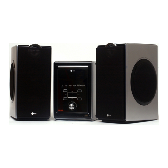
Related Manuals for LG LFS-U850


Summarization of Contents
Section 1. General
Servicing Precautions
Guidelines and precautions for servicing the Hi-Fi system, focusing on pick-up handling.
ESD Precautions
Techniques to reduce damage to components from static electricity.
Specifications
Technical specifications for the LG Micro Hi-Fi System models.
Section 2. Electrical Section
Troubleshooting Guide
Flowcharts for diagnosing and resolving electrical issues in the system.
Internal Block Diagram of ICs
Block diagrams illustrating the internal structure of key integrated circuits.
Pin Descriptions
Detailed descriptions of the pins for various integrated circuits used in the system.
Block Diagram
Overall system block diagram showing interconnections between major components.
Main Schematic Diagram
Detailed circuit schematic of the main board for the Hi-Fi system.
Front Schematic Diagram
Circuit schematic detailing the front panel and associated components.
SMPS Schematic Diagram
Circuit schematic for the Switching Mode Power Supply (SMPS) unit.
CD Part
Details regarding the CD component, including the WMA module.
USB Part
Schematics and diagrams related to the USB interface functionality.
WMA + USB Block Diagram
Block diagram illustrating the combined functionality of WMA and USB components.
Wiring Diagrams
Diagrams showing the physical wiring connections between different assemblies.
Main P.C. Board (Component Side)
Component layout view of the main printed circuit board.
Main P.C. Board (Solder Side)
Solder side view of the main printed circuit board, showing connections.
SMPS P.C. Board
Printed circuit board layout for the Switching Mode Power Supply.
Front P.C. Board
Printed circuit board layout and component placement for the front assembly.
CD P.C. Board (Component Side)
Component layout of the CD printed circuit board.
CD P.C. Board (Solder Side)
Solder side view of the CD printed circuit board.
Section 3. Exploded Views
Cabinet and Main Frame Section
Exploded view illustrating the cabinet and main frame components.
Deck Mechanism Exploded View
Exploded view showing the components of the CD deck mechanism.
Need help?
Do you have a question about the LFS-U850 and is the answer not in the manual?
Questions and answers