Table of Contents
Advertisement
Quick Links
RTKA489110DE0000BU
The
RAA489110
is a configurable buck-boost Narrow
Output Voltage DC (NVDC) and Hybrid Power
Buck-Boost (HPBB/Bypass) combo charger that uses
the advanced Renesas R3™ Technology to provide
high light-load efficiency, fast transient response, and
seamless DCM/CCM transitions for a variety of
mobile and industrial applications.
In Charge mode, the RAA489110 takes input power
from a wide range (4V to 30V) of DC power sources
(such as conventional AC/DC charger adapters, USB
PD ports, travel adapters) and safely charges battery
packs with up to four cells in a series configuration.
The RAA489110 supports On-the-Go (OTG)
functionality from 2-cell and 4-cell battery
applications. When OTG function is enabled, the
RAA489110 operates in Reverse Buck mode to
provide 5V at the USB port.
Serial communication through SMBus/I
programming of many critical parameters to deliver a
customized solution. These programming parameters
include, but are not limited to, adapter current limit,
charger current limit, system voltage setting, and
trickle charging current limit.
The RTKA489110DE0000BU evaluation board
demonstrates the performance of the RAA489110.
From the PROG pin to GND, a resistor can be used to
program the default value numbers of the battery in
series, the switching frequency, and the adapter
current limit charging function. The default value
numbers can also be set by SMBus.
Specifications
▪ V
= 3.9V to 30V (no dead zone)
IN
▪ V
= 3.9V to 18.304V
OUT
▪ MAX I
up to 6A
charge
R16UZ0064EU0101 Rev.1.01
Feb 24, 2023
Features
▪ Buck-boost NVDC or hybrid power (turbo boost)
▪ Bypass mode supported to connect system to
▪ Autonomous charging option (automatic end of
▪ Adapter current and battery current monitor
▪ PROCHOT# open-drain output, IMVP compliant
▪ Allows trickle charging of depleted battery
▪ System power monitor PSYS output, IMVP8/9
▪ Internal 8-bit ADC for monitoring key parameters
▪ USB-C PD Fast Role Swap support and PPS
2
C allows
▪ Independent compensation pins for forward and
▪ Supports supplemental power (Intel VMIN active
▪ Ideal diode control in Turbo mode
▪ Two-level adapter current limit available
▪ Battery Ship mode: IC ultra-low power state
▪ Supports programmable temperature profile
▪ SMBus and auto-increment I
Evaluation Board Manual
charger for 2-, 3-, or 4-cell Li-ion batteries using all
N-MOSFET transistors
adapter
charging)
(AMON/BMON)
compliant
support
reverse operation (OTG) modes
protection)
compliance using an NTC
© 2023 Renesas Electronics
2
C compatible
Page 1
Advertisement
Table of Contents

Subscribe to Our Youtube Channel
Related Manuals for Renesas RTKA489110DE0000BU


Summary of Contents for Renesas RTKA489110DE0000BU
- Page 1 ▪ Buck-boost NVDC or hybrid power (turbo boost) Buck-Boost (HPBB/Bypass) combo charger that uses charger for 2-, 3-, or 4-cell Li-ion batteries using all the advanced Renesas R3™ Technology to provide N-MOSFET transistors high light-load efficiency, fast transient response, and ▪...
- Page 2 RTKA489110DE0000BU Evaluation Board Manual BYPSRC VADP VSYS BYPSG CSIN NGATE CSIP CSOP BYPSG BYPSRC CSON RAA489110 ACOK BGATE PROCHOT# AMON/BMON VBAT 2S-4S CMOUT/INT# Battery OTGEN/CMIN PSYS BATGONE/NTC PSYS Figure 1. NVDC Plus HPBB Simplified Application Diagram Recommended Equipment ▪ 0V to 40V power supply with at least 6A source current capability ▪...
-
Page 3: Table Of Contents
Configuring the RTKA489110DE0000BU for Trickle Charging Mode ....10 1.3.5 Configuring the RTKA489110DE0000BU for OTG Mode ......10 1.3.6 Configuring the RTKA489110DE0000BU for Bypass Mode . -
Page 4: Functional Description
The RTKA489110DE0000BU evaluation board provides all circuits required to evaluate the features of the RAA489110. A majority of the features of the RAA489110 are available on the RTKA489110DE0000BU, such as adjustable output voltage, On-the-Go (OTG) mode, Trickle Charging mode for a depleted battery, and system power monitor at Buck, Boost, and Buck-Boost modes. -
Page 5: Installing The Usb Driver
RTKA489110DE0000BU Evaluation Board Manual Figure 3. RAA489110 Control Software Installer 4. To complete the software installation, follow the instructions to accept both End User License Agreements. 5. Click Close Menu from the installation wizard. 1.1.4 Installing the USB Driver This process explains how to install the SMBus to USB interface driver. The driver supports Microsoft Vista, Windows 7, Windows 8, and Windows 8.1 operating systems. -
Page 6: Using The Gui
Connect the RTKA489110DE0000BU to a power supply before using the SMBus GUI. 1.2.1 Setting the USB Connection Connect the USB cable from the USB of the computer port to the connector J10 of the RTKA489110DE0000BU. 1.2.2 Starting the GUI →... -
Page 7: Troubleshooting The Gui
▪ Make sure the driver files for the USB interface are installed correctly. The driver files are in the USB-I2C Driver folder. ▪ Check the USB cable connections from the RTKA489110DE0000BU to the USB port of the computer. ▪ Try different sequences: plug in the RTKA489110DE0000BU first or start the GUI first. -
Page 8: Regulating System Voltage
Charging mode, trickle Charging mode, and OTG mode. Figure 7 shows the top view of the RTKA489110DE0000BU and highlights the key testing points and connection terminals. For more information about the RAA489110, including other operation modes, refer to the RAA489110 datasheet. (-) Supply Lead... -
Page 9: Configuring The Rtka489110De0000Bu For Charging Mode
2. Set the battery emulator voltage to 7.8V, and connect the battery emulator output to battery leads J5 and J6. 3. Connect the USB cable at the USB port for the SMBus. LED1, LED2, and LED3 turn on. 4. Turn on the power supply. LED3 turns off. Next, turn on the battery emulator and open the Renesas RAA489110 GUI (Figure Figure 8. -
Page 10: Configuring The Rtka489110De0000Bu For Trickle Charging Mode
Note: Make sure the input current does not reach the input current limit value, especially for a small VADP input. 1.3.4 Configuring the RTKA489110DE0000BU for Trickle Charging Mode 1. Complete steps one through five in Configuring the RTKA489110DE0000BU for Charging Mode without any changes. - Page 11 RTKA489110DE0000BU Evaluation Board Manual Figure 9. OTGVoltage and OTGCurrent Settings in GUI 5. Select the Control0 & 1 Registers tab. 6. In the Control1 Register column, select 1: Enable in OTG Function to enable OTG, then click Write. See Figure R16UZ0064EU0101 Rev.1.01...
-
Page 12: Configuring The Rtka489110De0000Bu For Bypass Mode
1.3.6 Configuring the RTKA489110DE0000BU for Bypass Mode Refer to the RAA489110 datasheet for information about how to transition between different NVDC and Bypass modes. The document also provides steps on how to enable charging in each mode and how to allow the battery to supplement the adapter in Bypass mode (reverse turbo boost). -
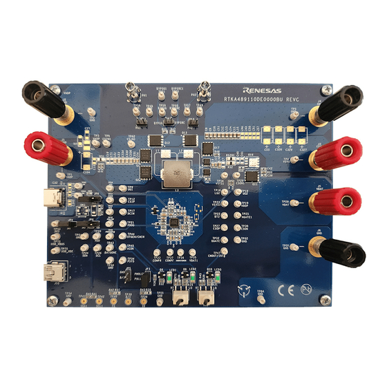
Page 13: Board Design
RTKA489110DE0000BU Evaluation Board Manual Board Design Figure 11. RTKA489110DE0000BU Evaluation Board (Top) Figure 12. RTKA489110DE0000BU Evaluation Board (Bottom) R16UZ0064EU0101 Rev.1.01 Page 13 Feb 24, 2023... -
Page 14: Layout Guidelines
Pin # Pin Name Layout Guidelines Connect this ground pad to the ground plane through a low impedance path. Renesas recommends Bottom using at least five vias to connect to ground planes in the PCB to ensure sufficient thermal dissipation directly under the IC. - Page 15 PHASE1 Run these two traces in parallel fashion with sufficient width. Avoid any sensitive analog signal trace from crossing over or getting close. Renesas recommends routing the PHASE1 trace to the high-side MOSFET drain pin instead of general copper. Place the IC close to the switching MOSFETs gate terminals and keep the gate drive signal traces short for a clean MOSFET drive.
- Page 16 RTKA489110DE0000BU Evaluation Board Manual Pin # Pin Name Layout Guidelines AMON/BMON No special consideration. Place the optional R-C filter in the general proximity of the controller. Signal pin, current source output. No special consideration. REFADJ is an analog signal pin for PSYS(REFADJ) feedback of the output voltage.
-
Page 17: Schematic Diagrams
Add push button symbol here - connect one end to the diode and the other end to ground TP46 100K TP47 TP48 TP49 TP50 TP51 TP52 TP54 TP55 SDA, SCL, ACOK, PROCHOT#, BATGONE, OTGPG/CMOUT, OTGEN all have 3V3 or VDD pull up options Figure 13. RTKA489110DE0000BU Schematic... -
Page 18: Bill Of Materials
RTKA489110DE0000BU Evaluation Board Manual Bill of Materials Reference Manufacturer Description Manufacturer Designator Part Number C1, C2, C3, C4 CAP TANT POLY 15µF 25V 1411 Vishay Sprague T55B156M025C0100 C37, C81, C83, CAP CER 1µF 25V X5R 0603 Murata Electronics GRM188R61E105KAADD C337, C338... - Page 19 RTKA489110DE0000BU Evaluation Board Manual Alpha & Omega Q12, Q13 MOSFET N-CH 30V 13A/30A 8DFN AON6414A Semiconductor Inc. RS1, RS2, Panasonic Electronic RES 0.01Ω 1% 1W 1206 ERJ-8CWFR010V RS201 Components Thermistor NTC 10KΩ 3380K 0603 Murata Electronics NCP18XH103F03RB R1, R14 RES 2Ω 1% 1/10W 0603...
- Page 20 RTKA489110DE0000BU Evaluation Board Manual TP1, TP2, TP3, TP4, TP5, TP6, TP9, TP10, TP11, TP12, TP15, TP16, TP17, TP18, TP19, TP20, TP21, TP22, TP23, TP24, TP25, TP26, TP27, TP28, TP29, TP30, TP31, TP32, TP33, TP34, TP35, TP36, PC Test Point Miniature White...
-
Page 21: Board Layout
RTKA489110DE0000BU Evaluation Board Manual Board Layout Figure 14. Silkscreen Top Layer Figure 15. Inner Layer 1 Figure 16. Inner Layer 2 Figure 17. Inner Layer 3 R16UZ0064EU0101 Rev.1.01 Page 21 Feb 24, 2023... -
Page 22: Typical Performance Graphs
RTKA489110DE0000BU Evaluation Board Manual Figure 18. Inner Layer 4 Figure 19. Bottom Layer (Mirror Image) Typical Performance Graphs 400μs/Div 400μs/Div Figure 20. Boost Mode Transitions: Output Voltage Loop Figure 21. Boost Mode Transitions: Charge Current to/from Adapter Current Loop. VADP = 5V, VBAT = 7V, Loop to/from Adapter Current Loop. - Page 23 RTKA489110DE0000BU Evaluation Board Manual 400μs/Div 400μs/Div Figure 22. Buck_Boost Mode Transitions: Output Figure 23. Buck_Boost Mode Transitions: Charge Voltage Loop to/from Adapter Current Loop. VADP = 9V, Current Loop to/from Adapter Current Loop. VADP = 9V, VBAT = 8.4V, MaxSystemVoltage = 8.8V, VBAT = 8.4V, MaxSystemVoltage = 8.8V,...
- Page 24 RTKA489110DE0000BU Evaluation Board Manual 400μs/Div 400μs/Div Figure 26. Buck Mode Transitions: Output Voltage Loop Figure 27. Buck Mode Transitions: Charge Current Loop to/from Adapter Current Loop. VADP = 28V, to/from Adapter Current Loop. VADP = 28V, VBAT = 15.5V, MaxSystemVoltage = 16.768V, VBAT = 15.5V, MaxSystemVoltage = 16.768V,...
- Page 25 RTKA489110DE0000BU Evaluation Board Manual 400μs/Div 400μs/Div Figure 30. OTG Mode Enable Using OTGEN Pin. Figure 31. OTG Mode Transients. VBAT = 8V, VOTG = 5V, VBAT = 8V, VOTG = 5V, General-Purpose Comparator OTG Current = 4A, SystemLoad: 0.5 <=> 3A Disabled, OTGEN Control Bit Enabled 400μs/Div...
-
Page 26: Ordering Information
RTKA489110DE0000BU Evaluation Board Manual Ordering Information Part Number Description RTKA489110DE0000BU RAA489110 evaluation board Revision History Revision Date Description Updated GUI images: Figures 6, 10, 11, and 12. 1.01 Feb 24, 2023 Moved Using the GUI section into the Functional Description section. - Page 27 Renesas' products are provided only subject to Renesas' Terms and Conditions of Sale or other applicable terms agreed to in writing. No use o any Renesas resources expands or otherwise alters any applicable warranties or warranty disclaimers for these products.
Need help?
Do you have a question about the RTKA489110DE0000BU and is the answer not in the manual?
Questions and answers