Table of Contents
Advertisement
Quick Links
R9A02G021
Fast Prototyping Board for R9A02G021 Microcontroller
FPB-R9A02G021
User's Manual
All information contained in these materials, including products and product specifications, represents
information on the product at the time of publication and is subject to change by Renesas Electronics
Corp. without notice. Please review the latest information published by Renesas Electronics Corp.
through various means, including the Renesas Electronics Corp. website (http://www.renesas.com).
Rev.1.00 Oct 2023
www.renesas.com
Advertisement
Table of Contents

Subscribe to Our Youtube Channel
Related Manuals for Renesas R9A02G021


Summary of Contents for Renesas R9A02G021
- Page 1 All information contained in these materials, including products and product specifications, represents information on the product at the time of publication and is subject to change by Renesas Electronics Corp. without notice. Please review the latest information published by Renesas Electronics Corp.
- Page 2 Renesas Electronics disclaims any and all liability for any damages or losses incurred by you or any third parties arising from the use of any Renesas Electronics product that is inconsistent with any Renesas Electronics data sheet, user’s manual or other Renesas Electronics document.
- Page 3 Unit Products The following usage notes are applicable to all Microprocessing unit and Microcontroller unit products from Renesas. For detailed usage notes on the products covered by this document, refer to the relevant sections of the document as well as any technical updates that have been issued for the products.
- Page 4 Renesas or its affiliates shall in no event be liable for any loss of profit, loss of data, loss of contract, loss of business, damage to reputation or goodwill, any...
-
Page 5: Table Of Contents
Debug and Programming ........................20 5.2.1 J-Link Emulator On-Board ........................21 5.2.2 External Debugger ..........................22 5.2.3 Settings in e studio and Renesas Flash Programmer ............... 23 Ecosystem ............................. 24 5.3.1 Seeed Grove Connector ........................26 ® 5.3.2 Digilent Pmod™ Connectors ....................... 27 5.3.3... - Page 6 Figure 3. FPB-R9A02G021 Board ........................6 Figure 4. FPB-R9A02G021 Board Block Diagram ..................7 Figure 5. Reference number for components on the FPB-R9A02G021 board (top side) ....... 8 Figure 6. Reference number for components on the FPB-R9A02G021 board (bottom side) ......8 Figure 7.
- Page 7 Table 17. Arduino Uno Connections ......................31 Table 18. FPB-FPB-R9A02G021 Board LED Functions ................33 Table 19. FPB-R9A02G021 Board Switches ....................34 Table 20. Remote Control Signal Receiver ....................36 Table 21. FPB-R9A02G021 Board Design Package Contents ..............39 R20UT5279EJ0100 Rev.1.00 Page 3 of 40 Oct.31.23...
-
Page 8: Board Overview
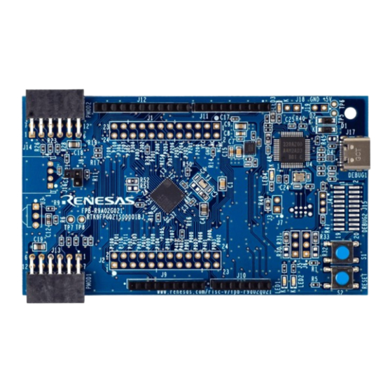
The FPB-R9A02G021, a Fast Prototyping Board for the R9A02G021 MCU, enables users to seamlessly evaluate the features of the R9A02G021 MCU and develop embedded systems applications using the e studio IDE. The on-board features along with a choice of popular ecosystem add-on modules brings user big ideas to life. -
Page 9: Assumptions And Advisory Notes
Arduino Uno User LEDs Connectors (Power and Analog) Figure 1. FPB-R9A02G021 Board Top Side Figure 2. FPB-R9A02G021 Board Bottom Side 1.1 Assumptions and Advisory Notes 1. It is assumed that the user has a basic understanding of microcontrollers and embedded systems hardware. -
Page 10: Box Contents
3. Printed information for China RoHS Figure 3. FPB-R9A02G021 Board 3. Ordering Information • FPB-R9A02G021 v1 kit orderable part number: RTK9FPG021S00001BJ Note: The underlined character in the orderable part number represents the kit version. R20UT5279EJ0100 Rev.1.00 Page 6 of 40... -
Page 11: Hardware Architecture And Default Configuration
4. Hardware Architecture and Default Configuration 4.1 Board Architecture The FPB-R9A02G021 board is designed with an architecture similar to other boards in the Renesas FPB series. Alongside the MCU there is an on-board programmer / debugger, pin headers for access to all the pins on the MCU, a power supply regulator, some LEDs and switches, and several ecosystem I/O connectors (Grove, Pmod and Arduino). -
Page 12: Component Placement Location And Dimension
4.3 Component Placement Location and Dimension Reference number for components on the FPB-R9A02G021 board is shown below. Figure 5. Reference number for components on the FPB-R9A02G021 board (top side) Figure 6. Reference number for components on the FPB-R9A02G021 board (bottom side) R20UT5279EJ0100 Rev.1.00... -
Page 13: Figure 7. Dimensional Drawing
R9A02G021 FPB-R9A02G021 User's Manual Dimensional drawing for the FPB-R9A02G021 board is shown below. 25.460 mm 30.540 mm 44.256 mm 53.400 mm 66.100 mm 95.000 mm Figure 7. Dimensional drawing R20UT5279EJ0100 Rev.1.00 Page 9 of 40 Oct.31.23... -
Page 14: Jumper Settings
4.4.2 Traditional Pin Header Jumpers These jumpers are traditional small pitch jumpers that require an external shunt to open/close them. The traditional pin jumpers on the FPB-R9A02G021 board are 0.1” (2.54 mm) pitch headers and require compatible 2.54 mm shunt jumpers. -
Page 15: Table 2. Default Jumper Settings For The Mcu
R9A02G021 FPB-R9A02G021 User's Manual Table 2. Default Jumper Settings for the MCU Location Circuit Group Default Function (Open / Closed) (Fitted / Not fitted) Open Closed: P003 (AVREFM) connects to breakout pin header J2. (Remove capacitor C3 at closed) Open: P003 (AVREFM) disconnects from breakout pin header J2. -
Page 16: Table 3. Default Jumper Settings For J-Link Ob And External Debugger
Function (Open / Closed) (Fitted / Not fitted) J-Link OB Not fitted Fitted (closed): J-Link Emulator On-board is held in reset. (R9A02G021 MCU free-running operation.) Not fitted (open): J-Link Emulator On-board is enabled. External Closed Closed: Debugger, P300 (TCKC) connects to the connector for external debugger J15 (TCKC) and J-Link Emulator On-board. -
Page 17: Table 4. Default Jumper Settings For Arduino Uno
R9A02G021 FPB-R9A02G021 User's Manual Table 4. Default Jumper Settings for Arduino Uno Location Circuit Group Default Function (Open / Closed) Arduino Uno Closed Closed: P105 (ANI18) connects to Arduino Uno (A4). Open: P105 (ANI18) disconnects from Arduino Uno (A4). Arduino Uno... - Page 18 R9A02G021 FPB-R9A02G021 User's Manual Location Circuit Group Default Function (Open / Closed) Arduino Uno Open Closed: P303 (TO04) connects to Arduino Uno (D10 / SS / PWM). Open: P303 (TO04) disconnects from Arduino Uno (D10 / SS / PWM). Arduino Uno...
-
Page 19: Table 5. Default Jumper Settings For Pmod 1
R9A02G021 FPB-R9A02G021 User's Manual Table 5. Default Jumper Settings for Pmod 1 Location Circuit Group Default Function (Open / Closed) (Fitted / Not fitted) Pmod 1 Closed Closed: P102 (RXD2 / SI20) connects to Pmod 1 (RXD / MISO / SCL). -
Page 20: Table 6. Default Jumper Settings For Pmod 2
R9A02G021 FPB-R9A02G021 User's Manual Table 6. Default Jumper Settings for Pmod 2 Location Circuit Group Default Function (Open / Closed) (Fitted / Not fitted) Pmod 2 Closed Closed: P108 (IRQ4_B) connects to Pmod 2 (CTS / INT). Open: P108 (IRQ4_B) disconnects from Pmod 2 (CTS / INT). -
Page 21: Table 7. Default Jumper Settings For Grove
R9A02G021 FPB-R9A02G021 User's Manual Table 7. Default Jumper Settings for Grove Location Circuit Group Default Function (Open / Closed) Grove Open Closed: P105 (ANI18) connects to Grove (SCL / AN). Open: P105 (ANI18) disconnects from Grove (SCL / AN). Grove... -
Page 22: System Control And Ecosystem Access
5.1 Power The FPB-R9A02G021 board is designed for +5 V operation. An on-board Linear Regulator is used to convert the +5 V supply to a +3.3 V supply. The +3.3 V supply is used to power the MCU and other peripheral features. -
Page 23: Power Supply Considerations
Pmod 1 and Pmod 2. Note: The maximum current that could be supplied to the FPB-R9A02G021 board is 1 A. Please be aware that the larger the current is, the higher the temperature of reverse current protection diode and +3.3V linear regulator will be. -
Page 24: Debug And Programming
The built-in J-Link Emulator On-Board debugger or an external debugger can be used also for programming to the FPB-R9A02G021 board. The FPB-R9A02G021 board can be programmed using VCOM of the built-in J-Link Emulator On-Board debugger (UART Boot via VCOM mode) or an external debugger (UART Boot via External Debugger mode). -
Page 25: J-Link Emulator On-Board
J17-B1_A12 GND [1] The yellow LED4, shows the visual status of the debug interface. When the FPB-R9A02G021 board is powered on, and LED4 is blinking, it indicates that the J-Link Emulator On-Board debugger is not connected to a host PC. When LED4 stays on, it indicates that it is connected to a host PC. -
Page 26: External Debugger
R9A02G021 FPB-R9A02G021 User's Manual 5.2.2 External Debugger The 20-pin 1.27 mm pitch SMD connector at J15 (not fitted) supports cJTAG interface and UART boot. This connector may be used for external debug of the MCU. Table 12. External Debugger Connection... -
Page 27: Settings In E 2 Studio And Renesas Flash Programmer
Figure 11. e Studio Settings FPB-R9A02G021 needs to be configured in UART Boot via VCOM shown in Table 9 when the MCU is re- programmed at UART Boot via VCOM mode with Renesas Flash Programmer. Figure 12 shows the settings for Renesas Flash Programmer when creating a new project for the FPB-R9A02G021 board. -
Page 28: Ecosystem
Note.2: Third party add-on modules may not be able to connect the FPB-R9A02G021 board simultaneously because the MCU pins which are connected to third party add-on modules are multiplexed. -
Page 29: Table 13. Mcu And Ecosystem Connection
R9A02G021 FPB-R9A02G021 User's Manual Table 13. MCU and Ecosystem Connection Ecosystem Misc. I/O Port Pmod 1 Pmod 2 Grove Arduino (LED, Switch, IR Receiver) P201 P202 IR Receiver Module P204 RESET P205 GPIO P206 GPIO P307 GPIO P303 P304 P305... -
Page 30: Seeed Grove Connector
Alternatively, this port can be configured to support two analog (ADC) inputs. The signals connected to Grove connector are shared with other ecosystem connectors. See Table 13 and FPB-R9A02G021 board schematic in detail. Table 14. Seeed Grove Connector Seeed Grove Connector... -
Page 31: Digilent Pmod™ Connectors
GPIO / CS3 P206 J13-11 J13-12 +3.3 V +5 V *1: The signals are shared with other ecosystem connectors. See Table 13 and FPB-R9A02G021 board schematic in detail. Pin 6 Pin 1 Pin 12 Pin 7 Figure 15. Pmod 1 Connector The default setting of the Pmod 1 interface supports +3.3 V devices. -
Page 32: Figure 16. Pmod 1 Copper Jumpers (Bottom Side)
Table 15. The copper jumpers are shown in Figure 16. Note: Exercise caution while modifying power source trace jumpers, E43 and E45. Permanent damage to the FPB-R9A02G021 board and/or connected modules may result. Figure 16. Pmod 1 Copper Jumpers (bottom side) R20UT5279EJ0100 Rev.1.00... -
Page 33: Figure 17. Pmod 2 Connector
J14-11 J14-12 +3.3 V +5 V *1: The signals are shared with other ecosystem connectors, user switches and IR receiver module. See Table 13 and FPB-R9A02G021 board schematic in detail. Pin 6 Pin 1 Pin 12 Pin 7 Figure 17. Pmod 2 Connector The default setting of the Pmod 2 interface supports +3.3 V devices. -
Page 34: Figure 18. Pmod 2 Copper Jumpers (Bottom Side)
Table 16. The copper jumpers are shown in Figure 18. Note: Exercise caution while modifying power source trace jumpers, E44 and E46. Permanent damage to the FPB-R9A02G021 board and/or connected modules may result. Figure 18. Pmod 2 Copper Jumpers (bottom side) P202 (IRQ2_C / RIN0) of the MCU can be connected to OUT pin of the IR receiver module and Pmod 2 INT / GPIO (J14-Pin7). -
Page 35: Arduino ® Connector
P011 (SCLA1) *1: The signals are shared with other ecosystem connectors, user switches and LEDs. See Table 12 and FPB-R9A02G021 board schematic in detail. *2: The signal is shared with VCOM (RXD0_B). *3: By shorting the copper jumper connects J11-Pin4 to +3.3 V through 10kΩ. The copper jumper may be shorted when P100 is assigned to IRQ6_C. -
Page 36: Figure 20. Arduino Uno Connectors
R9A02G021 FPB-R9A02G021 User's Manual AREF D13 / SCK IOREF D12 / MISO RESET D11 / MOSI / PWM 3.3 V D10 / SS / PWM D9 / PWM VIN (NC) D6 / PWM D5 / PWM D3 / INT / PWM... -
Page 37: Miscellaneous
R9A02G021 FPB-R9A02G021 User's Manual 5.4 Miscellaneous 5.4.1 LED Four LEDs are provided on the FPB-R9A02G021 board. Functions of the LEDs on the FPB-R9A02G021 board is described in the following table. Table 18. FPB-FPB-R9A02G021 Board LED Functions Reference number Color Function... -
Page 38: User And Reset Switches
5.4.2 User and Reset Switches Two miniature, momentary, mechanical push-button type SMD switches are mounted on the FPB- R9A02G021 board. Pressing the reset switch (S2) generates a reset signal to restart the MCU. Table 19. FPB-R9A02G021 Board Switches Reference number Function MCU Control Port... -
Page 39: Mcu Boot Mode
R9A02G021 FPB-R9A02G021 User's Manual Figure 26. User Switch S1 Copper Jumper (bottom side) 5.4.3 MCU Boot Mode A two-pin header (J8) can be fitted to select the boot mode (P203) of the MCU. For normal operation (single- chip mode), leave J8 open. To enable UART boot mode, place a shunt jumper on J8. -
Page 40: Special Feature Access
6. Special Feature Access 6.1 Remote Control Signal Receiver The FPB-R9A02G021 Board can be equipped with IR Receiver Module for remote control receive function. TSOP32438 (VISHAY) might be used for the FPB-R9A02G021 board. Refer to the manufacturer website for specification of the IR Receiver Module. -
Page 41: Mcu Native Pin Access
MCU power port. Each header pin is labelled with the voltage or port connected to that pin. Refer to the R9A02G021 MCU User’s Manual: Hardware for details of each port function, and the FPB- R9A02G021 board schematic for pin header port assignments. -
Page 42: Certifications
R9A02G021 FPB-R9A02G021 User's Manual 8. Certifications The FPB-R9A02G021 board meets the following certifications/standards. See page 4 of this user’s manual for the disclaimer and precautions. 8.1 EMC/EMI Standards • Innovation, Science and Economic Development Canada ICES-003 Compliance: CAN ICES-3 (A)/NMB-3(A) •... -
Page 43: Design And Manufacturing Information
R9A02G021 FPB-R9A02G021 User's Manual 9. Design and Manufacturing Information The design and manufacturing information for the FPB-R9A02G021 kit is available in the “FPB-R9A02G021 Design Package” available on renesas.com/risc-v/fpb-r9a02g021. Design package file name: fpb-r9a02g021-v1-designpackage.zip • Design package contents • Table 21. FPB-R9A02G021 Board Design Package Contents... -
Page 44: Revision History
R9A02G021 FPB-R9A02G021 User's Manual Revision History Rev. Date Description Page Summary 1.00 Oct.31.23 — Initial release R20UT5279EJ0100 Rev.1.00 Page 40 of 40 Oct.31.23... - Page 45 FPB-R9A02G021 User's Manual Publication Date: Oct.31.23 Published by: Renesas Electronics Corporation...
- Page 46 FPB-R9A02G021 User's Manual R20UT5279EJ0100...
Need help?
Do you have a question about the R9A02G021 and is the answer not in the manual?
Questions and answers