Table of Contents
Advertisement
Quick Links
Advertisement
Table of Contents

Related Manuals for Fibocom NL652-EU-00 Series


Summary of Contents for Fibocom NL652-EU-00 Series
- Page 1 FIBOCOM NL652-EU-00 Series Hardware User Manual Version: V1.0.1 Date: 2019-12-06 69100.1000.00.02.61.34_DEMO" Reproduction forbidden without Fibocom Wireless Inc. written authorization - All Rights Reserved. FIBOCOM NL652-EU-00 Series Hardware User Manual Page 1 of 50...
- Page 2 Applicability type Product model Description NL652-EU-00 MCP is 4+2,support MAIN_ANT, DIV_ANT Reproduction forbidden without Fibocom Wireless Inc. written authorization - All Rights Reserved. FIBOCOM NL652-EU-00 Series Hardware User Manual Page 2 of 50...
- Page 3 Delete Network status indicate V1.0.1 2019-12-06 Tan Lefan Hu Wenkai Liu Ke function Delete sim card hot plug function Reproduction forbidden without Fibocom Wireless Inc. written authorization - All Rights Reserved. FIBOCOM NL652-EU-00 Series Hardware User Manual Page 3 of 50...
-
Page 4: Table Of Contents
Low Power Consumption ..................29 Flight mode ......................... 29 WAKEUP_OUT ......................29 Sleep mode ........................ 29 6.3.1 USB Suspend ........................ 29 Reproduction forbidden without Fibocom Wireless Inc. written authorization - All Rights Reserved. FIBOCOM NL652-EU-00 Series Hardware User Manual Page 4 of 50... - Page 5 Terms and acronyms ....................47 11.3 Related Document ...................... 49 11.4 Reference Standards ....................49 11.5 Contact ........................50 Reproduction forbidden without Fibocom Wireless Inc. written authorization - All Rights Reserved. FIBOCOM NL652-EU-00 Series Hardware User Manual Page 5 of 50...
- Page 6 Figure 9-2 Structure Dimension (Unit: mm) ..................40 Figure 9-3 Tray Packaging Process ....................42 Figure 9-4 Tray Size (Unit: mm) ....................... 43 Reproduction forbidden without Fibocom Wireless Inc. written authorization - All Rights Reserved. FIBOCOM NL652-EU-00 Series Hardware User Manual Page 6 of 50...
- Page 7 Table 10-2 Multilevel Multislot Allocation ..................46 Table 10-3 EGPRS Modulation and Encoding Method ..............46 Table 10-4 Terms and Acronyms ...................... 49 Reproduction forbidden without Fibocom Wireless Inc. written authorization - All Rights Reserved. FIBOCOM NL652-EU-00 Series Hardware User Manual Page 7 of 50...
-
Page 8: Introduction
Product manufacturers need to communicate the following safety instructions to end users. In case of failure to comply with these safety rules, Fibocom will not be responsible for the consequences caused by the user’s misuse. - Page 9 There is a safety hazard in operating electronic equipment in any potentially explosive environment. Reproduction forbidden without Fibocom Wireless Inc. written authorization - All Rights Reserved. FIBOCOM NL652-EU-00 Series Hardware User Manual Page 9 of 50...
-
Page 10: Product Overview
2 Product Overview 2.1 Product Introduction The NL652-EU-00 series wireless module is a broadband wireless terminal product applicable to various network formats and multi-bands include TDD-LTE/FDD-LTE/WCDMA/GSM. 2.2 Product Specification Specification LTE FDD: Band 1,3,5,7,8,20,28 LTE TDD: Band 38,40,41 Operating frequency... -
Page 11: Functional Diagram
When the temperature is beyond the normal operating temperature range (-30 °C to + 75 °C), the RF performance of the module may slightly exceed the 3GPP specification. 2.3 Functional Diagram Functional diagram shows the main hardware features of the NL652-EU-00 series module: W_DISABLE ... - Page 12 PMIC Baseband VBAT_BB (U)SIM GPIOs VDD_EXT STATUS PWRKEY RESET_N PCI Express M.2 Key-B interface Figure 2-1 Functional Diagram Reproduction forbidden without Fibocom Wireless Inc. written authorization - All Rights Reserved. FIBOCOM NL652-EU-00 Series Hardware User Manual Page 12 of 50...
-
Page 13: Functional Interface
3 Functional Interface 3.1 M.2 Key-B interface The NL652-EU-00 series module use M.2 Key-B standard interface and has 75 pins in total. Figure 3-1 Pin Assignment (Top View Diagram) Note: Notch is the breach of golden finger. The fucntions with * are in development. -
Page 14: Pin Function
Power output Analog input Analog output Open drain Open collector Table 3-1 I/O Description The pin function description of NL652-EU-00 series module is shown as follow table: Pin Name I/O Level Description Connected to GND internally. This module CONFIG_3 is configured as WWAN-SSIC-0. - Page 15 PCM output, PCM_OUT min=1.35V Reserved min=-0.3V max=0.3V Body SAR detection (1.8V), internal min=1.6V pull-up, active low max=2.0V RESERVED Reproduction forbidden without Fibocom Wireless Inc. written authorization - All Rights Reserved. FIBOCOM NL652-EU-00 Series Hardware User Manual Page 15 of 50...
- Page 16 Vmax=1.9V Vmin=1.7V (U)SIM power supply,module support USIM_VDD For 3.0V (U)SIM: 1.8V and 3V (U)SIM card Vmax=3.05V Vmin=2.7V max=50mA Reproduction forbidden without Fibocom Wireless Inc. written authorization - All Rights Reserved. FIBOCOM NL652-EU-00 Series Hardware User Manual Page 16 of 50...
- Page 17 I2C_SDA I2C data, pull up internally max=0.6V min=1.2V max=2.0V RESERVED RESERVED RESERVED RESERVED Reproduction forbidden without Fibocom Wireless Inc. written authorization - All Rights Reserved. FIBOCOM NL652-EU-00 Series Hardware User Manual Page 17 of 50...
- Page 18 Connected to GND internally. This CONFIG_2 module is configured as WWAN-SSIC-0. Table 3-2 Pin function description Note: Keep the unused pins floating. Reproduction forbidden without Fibocom Wireless Inc. written authorization - All Rights Reserved. FIBOCOM NL652-EU-00 Series Hardware User Manual Page 18 of 50...
-
Page 19: Electrical Characteristics
3,5,11,27,33,39,45,51,57,71,73 All GND pins must be grounded Table 4-1 Power Interface 4.2 Power supply The NL652-EU-00 series module needs to be powered by the VCC pin. The recommend power design is shown in Figure 4-1: Module VBAT Figure 4-1 Recommend Power Design... -
Page 20: Power Consumption
Table 4-2 Filter Capacitors Design of Power Supply The power stability can ensure the normal operation of NL652-EU-00 series module. Special attention requires when design circuit that the power supply ripple limit for the module is no more than 150mV (the circuit ESR <... - Page 21 EDGE Data transfer GSM850; PCL=8; EGPRS-RMS EDGE 1Rx/4Tx MCS9 EDGE Data transfer DCS1800; PCL=2; 1Rx/4Tx WCDMA Data transfer Band I WCDMA WCDMA-RMS Reproduction forbidden without Fibocom Wireless Inc. written authorization - All Rights Reserved. FIBOCOM NL652-EU-00 Series Hardware User Manual Page 21 of 50...
- Page 22 LTE TDD Data transfer Band 41 @+23dBm Table 4-3 Power Consumption Note: USB sleep should send AT command at+gtusbsleepen=1,1 Reproduction forbidden without Fibocom Wireless Inc. written authorization - All Rights Reserved. FIBOCOM NL652-EU-00 Series Hardware User Manual Page 22 of 50...
-
Page 23: Functional Interface
Table 5-1 Control Signal 5.1.1 Power on/off 5.1.1.1 Power on When NL652-EU-00 series module in power off mode, pull down FULL_CARD_POWER_OFF# pin 100ms~2s, the module will power on. Reference design show as follow Figure. High level power on Module... -
Page 24: Power Off
P FULL_CARD_POWER_OF# pin or AT commands, then cut off power supply. When power off by AT commands, please don’t pull down P FULL_CARD_POWER_OF# Reproduction forbidden without Fibocom Wireless Inc. written authorization - All Rights Reserved. FIBOCOM NL652-EU-00 Series Hardware User Manual... -
Page 25: Reset
Clients can control RESET# pin by two modes: OC/OD drive circuits and button switch. The reference circuit is shown in figure 5-4 and figure 5-5 respectively: Figure 5-4 OC Driven Reset Reference Circuits Reproduction forbidden without Fibocom Wireless Inc. written authorization - All Rights Reserved. FIBOCOM NL652-EU-00 Series Hardware User Manual Page 25 of 50... -
Page 26: U)Sim Card Interface
Restarting Resetting Figure 5-6 Reset Timing 5.2 (U)SIM card interface NL652-EU-00 series module has built-in (U)SIM card interface, and supports 1.8V and 3.0V (U)SIM card. 5.2.1 (U)SIM pin definition (U)SIM pin definition is shown in the following table: Pin name Pin Num. -
Page 27: U)Sim Design Requirements
USIM_CLK Clock Signal USIM_RESET Reset Signal Table 5-4 (U)SIM Card Pin NL652-EU-00 series module does not support SIM card hot plug function temporarily. Use (U)SIM card connector without detection signal, USIM_DETECT pin must keep floating. Module SIM card connector USIM_PWR... -
Page 28: Usb Interface
USIM_DATA should be pulled up to USIM_VDD with a 10K resistor. 5.3 USB interface NL652-EU-00 series modules support USB2.0, compatible with USB high-speed (480Mbits/s) and USB full-speed (12Mbits/s).Refer to the “Universal Serial Bus Specification 2.0” for USB Bus timing and electrical characteristics of modules. -
Page 29: Low Power Consumption
USB serial port driver supports selective suspend power management. Reproduction forbidden without Fibocom Wireless Inc. written authorization - All Rights Reserved. FIBOCOM NL652-EU-00 Series Hardware User Manual Page 29 of 50... -
Page 30: Sleep Wakeup
Configuration Pulse Width +GTPMTIME More sleep command description please refer to《FIBOCOM AT Commands User Manual_Sleep》 Reproduction forbidden without Fibocom Wireless Inc. written authorization - All Rights Reserved. FIBOCOM NL652-EU-00 Series Hardware User Manual Page 30 of 50... -
Page 31: Rf Interface
10MHz Bandwidth, 1 RB LTE FDD Band 5 23±1 10MHz Bandwidth, 1 RB Band 7 23±1 10MHz Bandwidth, 1 RB Reproduction forbidden without Fibocom Wireless Inc. written authorization - All Rights Reserved. FIBOCOM NL652-EU-00 Series Hardware User Manual Page 31 of 50... -
Page 32: Receive Sensitivity
The sensitivity of above table is the result of main and diversity test separately, if tested with PRX and DRX together, the result will rise about 3dB. Reproduction forbidden without Fibocom Wireless Inc. written authorization - All Rights Reserved. FIBOCOM NL652-EU-00 Series Hardware User Manual... -
Page 33: Antenna Design
It must use the most suitable antenna to adapt to the relevant frequency band. Bandwidth GSM900: 80 MHz (GSM/EDGE) GSM850: 70 MHz Reproduction forbidden without Fibocom Wireless Inc. written authorization - All Rights Reserved. FIBOCOM NL652-EU-00 Series Hardware User Manual Page 33 of 50... -
Page 34: Antenna Reference Design
In addition, the RF cable connect with antenna, and the location of the fixed antenna also may affect its performance. NL652-EU-00 series module’s three antenna all led by welding plate. Recommend the customer to use the antenna connector of the USS RF socket (fourth generation) RF coaxial connector and corresponding match adapter cable. - Page 35 Ground around antenna must be keep connect with main ground. For more design information please refer to《FIBOCOM RF Antenna Application Design Instruction》 Reproduction forbidden without Fibocom Wireless Inc. written authorization - All Rights Reserved. FIBOCOM NL652-EU-00 Series Hardware User Manual Page 35 of 50...
-
Page 36: Reliability
Operating voltage range is the normal working voltage range of the module, beyond which the module will have abnormal performance. 8.1.1 Absolute voltage range The absolute voltage range of NL652-EU-00 series module is shown as table 8-1. Interface Description... -
Page 37: Environmental Reliability Requirements
Table 8-4 Environmental Reliability Requirements 8.4 ESD characteristics NL652-EU-00 series module design has considered ESD issue and provided ESD protect measurements, but take ESD issue taken by module carrier and secondary development into consideration, developers should care ESD protection of module application terminal. In addition to considering anti-static treatment of packaging, please refer to recommended circuit of interface design in the document. - Page 38 Air discharge Contact discharge Antenna port ±8KV ±4KV Other port ±1KV ±0.5KV Table 8-5 ESD Allowable Discharge Rang Reproduction forbidden without Fibocom Wireless Inc. written authorization - All Rights Reserved. FIBOCOM NL652-EU-00 Series Hardware User Manual Page 38 of 50...
-
Page 39: Structure Specification
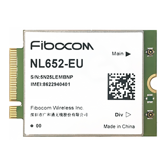
9 Structure specification 9.1 Product appearance The product appearance of NL652-EU-00 series module is shown in Figure 9-1: Figure 9-1 Product Appearance 9.2 Structure dimension The structure dimension of NL652-EU-00 series module is shown as Figure 9-2: Reproduction forbidden without Fibocom Wireless Inc. written authorization - All Rights Reserved. -
Page 40: Carrier And Storage
The module is a precision electronic product, and may suffer permanent damage if no correct electrostatic protection measures are taken. Reproduction forbidden without Fibocom Wireless Inc. written authorization - All Rights Reserved. FIBOCOM NL652-EU-00 Series Hardware User Manual Page 40 of 50... -
Page 41: Tray Package
6 boxes in each case. Tray packaging process is shown as follow Figure. Reproduction forbidden without Fibocom Wireless Inc. written authorization - All Rights Reserved. FIBOCOM NL652-EU-00 Series Hardware User Manual Page 41 of 50... -
Page 42: Tray Size
Figure 9-3 Tray Packaging Process 9.4.2 Tray size The pallet size of L850 module is 315*170*6.5mm, as shown in Figure 5-5: Reproduction forbidden without Fibocom Wireless Inc. written authorization - All Rights Reserved. FIBOCOM NL652-EU-00 Series Hardware User Manual Page 42 of 50... - Page 43 Figure 9-4 Tray Size (Unit: mm) Reproduction forbidden without Fibocom Wireless Inc. written authorization - All Rights Reserved. FIBOCOM NL652-EU-00 Series Hardware User Manual Page 43 of 50...
-
Page 44: Approval
NL652-EU-00 series module approval is shown as table 10-1: Certification Scheme NL652-EU-00 series module Table 10-1 Approval For more information, please refer to Fibocom website: http://www.fibocom.com.cn/ Reproduction forbidden without Fibocom Wireless Inc. written authorization - All Rights Reserved. FIBOCOM NL652-EU-00 Series Hardware User Manual Page 44 of 50... -
Page 45: Appendix
Active timeslots indicate the total number of timeslots that the GPRS device can use for both uplink and downlink communications. Multislot Class Downlink Slots Uplink Slots Active Slots Reproduction forbidden without Fibocom Wireless Inc. written authorization - All Rights Reserved. FIBOCOM NL652-EU-00 Series Hardware User Manual Page 45 of 50... - Page 46 179.2kbps MCS-8 8-PSK 54.4kbps 108.8kbps 217.6kbps MCS-9 8-PSK 59.2kbps 118.4kbps 236.8kbps Table 10-3 EGPRS Modulation and Encoding Method Reproduction forbidden without Fibocom Wireless Inc. written authorization - All Rights Reserved. FIBOCOM NL652-EU-00 Series Hardware User Manual Page 46 of 50...
-
Page 47: Terms And Acronyms
Secondary Cell for CA Mobile Equipment Mobile Station Mobile Terminated Printed Circuit Board Protocol Data Unit Phase Shift Keying Reproduction forbidden without Fibocom Wireless Inc. written authorization - All Rights Reserved. FIBOCOM NL652-EU-00 Series Hardware User Manual Page 47 of 50... - Page 48 Minimum Output High Level Voltage Value VOLmax Maximum Output Low Level Voltage Value VOLmin Minimum Output Low Level Voltage Value Reproduction forbidden without Fibocom Wireless Inc. written authorization - All Rights Reserved. FIBOCOM NL652-EU-00 Series Hardware User Manual Page 48 of 50...
-
Page 49: Related Document
3GPP TS 27.005 V10.0.1: Use of Data Terminal Equipment - Data Circuit terminating Equipment (DTE - DCE) interface for Short Message Service (SMS) and Cell Broadcast Service (CBS) Reproduction forbidden without Fibocom Wireless Inc. written authorization - All Rights Reserved. FIBOCOM NL652-EU-00 Series Hardware User Manual Page 49 of 50... -
Page 50: Contact
11.5 Contact URL:http://www.fibocom.com.cn/ HQ Address:5F Shekou Science and Technology Building, Nanhai Ave 1057, Shenzhen,Guangdong P.R.China TEL:+86 755-26733555 Fax:+86 755-26520841 Reproduction forbidden without Fibocom Wireless Inc. written authorization - All Rights Reserved. FIBOCOM NL652-EU-00 Series Hardware User Manual Page 50 of 50...
Need help?
Do you have a question about the NL652-EU-00 Series and is the answer not in the manual?
Questions and answers