Table of Contents
Advertisement
Quick Links
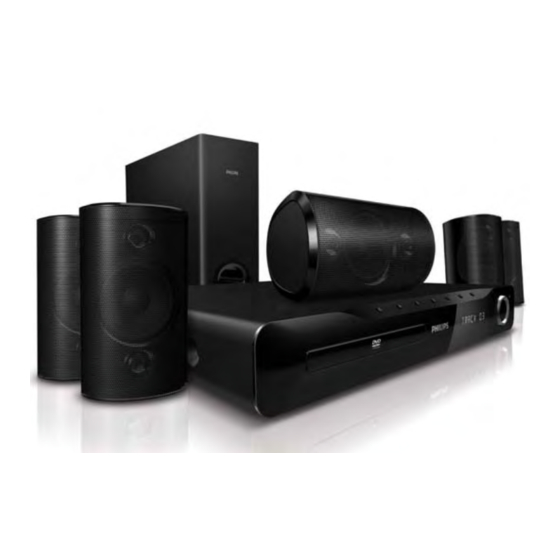
BD Home Theater System
Service
Service
Service
Service Manual
©
Copyright 2010 Philips Consumer Electronics B.V. Eindhoven, The Netherlands
All rights reserved. No part of this publication may be reproduced, stored in a retrieval system or
transmitted, in any form or by any means, electronic, mechanical, photocopying, or otherwise
without the prior permission of Philips.
Published by
RY_HF1029
Service Audio Printed in The Netherlands Subject to modification
Version 1.0
TABLE OF CONTENTS
Location of PCB Boards ............................................ 1-2
Versions Variation ...................................................... 1-2
Specifications ............................................................ 1-3
Measurement Setup .................................................. 1-4
Service Aids .............................................................. 1-5
ESD & Safety Instruction .......................................... 1-6
Lead-free soldering Information ................................ 1-7
Setting procedure & Repair Instructions........................ 2
Disassembly Instructions & Service positions .............. 3
Block & Wiring Diagram ................................................ 4
Quick Start Guide .......................................................... 5
VFD+VOL+USB+MP3 PCB .......................................... 6
MAIN PCB ...................................................................... 7
POWER PCB ................................................................ 8
BD PCB .......................................................................... 9
TOUCH PCB ................................................................ 10
Mechanical Exploded view .......................................... 11
Revision List ................................................................ 12
1 1
Chapter
HTS3260/12
3139 785 35500
GB
Advertisement
Table of Contents

Related Manuals for Philips HTS3260/12


Summary of Contents for Philips HTS3260/12
- Page 1 Revision List ..............12 © Copyright 2010 Philips Consumer Electronics B.V. Eindhoven, The Netherlands All rights reserved. No part of this publication may be reproduced, stored in a retrieval system or transmitted, in any form or by any means, electronic, mechanical, photocopying, or otherwise without the prior permission of Philips.
- Page 2 1 - 2 LOCATION OF PCB BOARDS BD PCB MAIN PCB TOUCH PCB POWER PCB VFD PCB Vol+USB+MP3 PCBB VERSION VARIATION: Type/Versions HTS3260 Features Output Power - 300W Voltage (220~240V) AUX/MP3 SERVICE SCNARIO MATRIX: HTS3260 Type/Versions Board in used Main Board Power Board VFD+VOL+USB+MP3 Board BD Board...
- Page 3 1 - 3 SPECIFICATIONS Playback media Subwoofer BD-Video, DVD-Video, DVD+R/+RW,DVD-R/-RW, DVD+R/- Impedance ............... 4 ohm R DL, CD-R/CDRW,Audio CD, Video CD/SVCD, PictureCD, Speaker drivers ........165 mm (6.5”) woofer MP3-CD, WMA-CD, DivX (Ultra)-CD, USB fl ash drive. Frequency response ..........40 Hz-150 Hz Dimensions (WxHxD) ......
- Page 4 1 - 4 MEASUREMENT SETUP Tuner FM Bandpass LF Voltmeter 250Hz-15kHz e g. PM2534 e.g. 7122 707 48001 RF Generator e.g. PM5326 S/N and distortion meter e.g. Sound Technology ST1700B Use a bandpass filter to eliminate hum (50Hz, 100Hz) and disturbance from the pilottone (19kHz, 38kHz). Use Audio Signal Disc SBC429 4822 397 30184 (replaces test disc 3)
- Page 5 1 - 5 SERVICE AIDS Service Tools: Universal Torx driver holder .........4822 395 91019 Torx bit T10 150mm ...........4822 395 50456 Torx driver set T6-T20 .........4822 395 50145 Torx driver T10 extended ........4822 395 50423 Compact Disc: SBC426/426A Test disc 5 + 5A ......4822 397 30096 SBC442 Audio Burn-in test disc 1kHz ....4822 397 30155 SBC429 Audio Signals disc .........4822 397 30184 Dolby Pro-logic Test Disc ........4822 395 10216...
- Page 6 1 - 6 WAARSCHUWING WARNING Alle IC’s en vele andere halfgeleiders zijn All ICs and many other semi-conductors are gevoelig voor electrostatische ontladingen susceptible to electrostatic discharges (ESD). (ESD). Careless handling during repair can reduce life Onzorgvuldig behandelen tijdens reparatie kan drastically.
- Page 7 • You will find this and more technical information Use only lead-free solder alloy Philips SAC305 with within the “magazine”, chapter “workshop news”. order code 0622 149 00106. If lead-free solder-paste is required, please contact the manufacturer of your For additional questions please contact your local solder-equipment.
- Page 8 Package version: 000029.0 version of your home theater with the latest software version (if available) on the Philips web site, and for BD-Live application and Software BE Close software update, make sure that the network router has access to...
- Page 9 2 - 2 2 - 2 c) Assembly Blu-ray Loader to “J802”,”J900”,”J906” on the top of e) Insert empty USB device of MSC type and press <OK> button j) If laser check fails press “ ” <Home> button and repeat OPU Software upgrade will take 5 minutes matching procedure.
- Page 10 2 - 3 2 - 3 REPAIR INSTRUCTIONS MAIN UNIT REPAIR CHART...
- Page 11 3 - 1 3 - 1 DISASSEMBLY INSTRUCTIONS Dismantling of theTop & Front Panel Assemble 3) Loosen 6 screws and remove the Top Cover by lifting the rear portion upwards before sliding it out towards the rear. - 4 screws “A” at the back panel as shown in fi gure 4. 1) Open the BD Tray by using the Open/Close Button while the Set is ON and disconnect the mains supply after removing the Tray - 1 screw “B”...
- Page 12 3 - 2 3 - 2 Dismantling of the VFD+VOL+USB+MP3 Board Dismantling of the MAIN Board 1) Loosen 6 screws “D” on the top of VFD+VOL+USB+MP3 Board as shown in fi gure 10. 1) Loosen 3 screws “ H ” on the top of MAIN Board as shown in fi gure 14. 2) Loosen 3 screws “...
- Page 13 3 - 3 3 - 3 SERVICE POSITIONS Note:In some service positions the components or copper patterns of one board may risk touching its neighbouring pc boards or metallic parts. To prevent such short-circuit use a piece of hard paper or other insulating material between them.
- Page 14 4 - 1 4 - 1 BLOCK DIAGRAM...
- Page 15 4 - 2 4 - 2 WIRING DIAGRAM...
- Page 16 5 - 1 5 - 1 QUICK START GUIDE User Manual SUBWOOFER SUBWOOFER FRONT FRONT RIGHT RIGHT FRONT FRONT FRONT FRONT CENTER CENTER LEFT LEFT REAR REAR RIGHT RIGHT REAR LEFT FM Antenna Power cord Audio/Video...
- Page 17 5 - 2 5 - 2 Audio/ Video Cable FRONT FRONT FRONT RIGHT LEFT CENTER SUBWOOFER REAR REAR RIGHT LEFT Antenna...
- Page 18 5 - 3 5 - 3 HOME THEATER HOME THEATER HOME THEATER...
- Page 19 5 - 4 MP3 Link Cable User Manual www.philips.com/support Speci? cations are subject to change without notice Trademarks are the property of Koninklijke Philips Electronics N.V. or their respective owners 2010 © Koninklijke Philips Electronics N.V. All rights reserved. sgsna 1015/12 v2...
- Page 20 6 - 1 6 - 1 FTD DISPLAY PIN ASSIGNMENT VFD+VOL+USB+MP3 BOARD TABLE OF CONTENTS FTD Display Pin Assignment ............. 6-1 Circuit Diagram ................. 6-2 PCB Layout Top & Bottom View ............6-3 PIN CONNECTION...
- Page 21 6 - 2 6 - 2 CIRCUIT DIAGRAM C810 C813 C816 C819 C822 CN810 B1 DP810 A2 IC810 R811 R814 R817 R820 R823 VR810 C1 ZD811 B2 C811 C814 C817 C820 C823 CN811 A1 FB810 B1 IC810 R812 R815 R818 R821 SN810 B1 VR810 C1...
- Page 22 6 - 3 6 - 3 PCB LAYOUT - TOP VIEW C810 C817 CN812 JP810 JP813 JP816 JP819 JP822 USB810 A3 C815 CN810 DP810 JP811 JP814 JP817 JP820 JP823 VR810 C816 CN811 JK810 JP812 JP815 JP818 JP821 SN810 CN810 CN812 PCB LAYOUT - BOTTOM VIEW C811 C814...
- Page 23 7- 1 7 - 1 INTERNAL IC DIAGRAM - STM32F100VBT6ATR MAIN BOARD TABLE OF CONTENTS Internal IC Diagram ................7-1 Circuit Diagram .................. 7-2 PCB Layout Top View ............... 7-3 PCB Layout Bottom View ..............7-4 INTERNAL IC DIAGRAM - CS5346-CQZR 3.3 V to 5 V 3.3 V Left PGA Output...
- Page 24 7 - 2 7 - 2 CIRCUIT DIAGRAM C1005 C2 C351 C499 D5007 C3 R106 R302 R504 C1008 D2 C352 C5011 B3 D5008 C3 R1065 D3 R303 R5040 C3 C1009 D2 C353 C5017 C2 D5015 B3 R1066 D3 R308 R5042 B3 C101 C354 C502...
- Page 25 7- 3 7 - 3 PCB LAYOUT - TOP VIEW C1005 C3 C117 C305 C351 C4031 B3 C455 C497 C516 C705 D1002 C1 FB5002 B4 IC5007 B3 L607 R1009 A1 R106 R1099 C2 R156 R190 R311 R359 R440 R480 R5064 A2 R5131 B3 R521 C101...
- Page 26 7 - 4 7 - 4 PCB LAYOUT - BOTTOM VIEW C5051 B3 C513 C5157 C3 C589 R1065 C3 R161 R282 R329 R466 R5065 B3 R5144A A4 R5282 A4 C1008 A2 C1015 C3 C105 C113 C243 C4001 A4 C4025 A4 C4042 A3 C462 C485...
- Page 27 8 - 1 8 - 1 INTERNAL IC DIAGRAM - SSC620S SOP POWER BOARD TABLE OF CONTENTS Internal IC Diagram ................8-1 Circuit Diagram .................. 8-2 PCB Layout Top View ............... 8-3 PCB Layout Bottom View ..............8-4 INTERNAL IC DIAGRAM - AZ7500BP OUTPUT CTRL Oscillator Pulse-Steering...
- Page 28 8 - 2 8 - 2 CIRCUIT DIAGRAM BD901 A1 C920 C931 C949 C960 C971 C982 CN905 C4 D917 D931 IC904 C2 Q902 Q915 R906 R919 R933 R946 R958 R969 R981 R995 ZD902 C2 C901 C921 C935 C950 C961 C972 C983 CN906 A4 D918...
- Page 29 8 - 3 8 - 3 PCB LAYOUT - TOP VIEW BD901 B4 C919 B4 C940 C3 C965 C2 C973 C1 C983 A1 CN906 A2 D922 B2 F901 IC904 C2 J907 J913 J919 J926 L902 NTC901 A4 Q912 B3 R940 C3 R958 C1 R991 C1 TVR902 C4...
- Page 30 8 - 4 8 - 4 PCB LAYOUT - BOTTOM VIEW C904 C928 C943 C951 C959 C981 C998 D910 IC901 C3 Q914 R902 R909 R919 R926 R938 R953 R961 R968 R976 R992 ZD902 C3 ZD910 B2 C905 C929 C944 C953 C964 C982 D903...
-
Page 31: Table Of Contents
9 - 1 9 - 1 BD BOARD TABLE OF CONTENTS Circuit Diagram (one) ................ 9-2 Circuit Diagram (two) ................ 9-3 Circuit Diagram (three) ..............9-4 Circuit Diagram (four) ............... 9-5 Circuit Diagram (fi ve) ................ 9-6 Circuit Diagram (six) ................. 9-7 Circuit Diagram (seven) .............. -
Page 32: Circuit Diagram (One)
9 - 2 9 - 2 CIRCUIT DIAGRAM (one) C966 CB12 A3 CE19 A2 CE23 B2 FB705 A1 FB719 B3 FB738 B2 Q518 B2 R472 R477 U908 C960 C971 CB13 A1 CE24 B3 FB710 B1 FB722 B3 FB742 A1 Q519 B2 R473 R478 C961... -
Page 33: Circuit Diagram (Two)
9 - 3 9 - 3 CIRCUIT DIAGRAM (two) C100 C104 C108 C112 C116 C120 C124 C128 C132 C136 C140 C144 C148 C152 C970 R101 R105 RN100 B3 RN104 C3 U102 C101 C105 C109 C113 C117 C121 C125 C129 C133 C137 C141 C145... -
Page 34: Circuit Diagram (Three)
9 - 4 9 - 4 CIRCUIT DIAGRAM (three) C200 C203 C206 C209 C212 C215 C218 C221 C224 C227 C230 C233 C236 C239 R202 R205 RN201 B3 RN204 B3 U202 C201 C204 C207 C210 C213 C216 C219 C222 C225 C228 C231 C234 C237... -
Page 35: Circuit Diagram (Four)
9 - 5 9 - 5 CIRCUIT DIAGRAM (four) C300 B2 C308 A1 C313 A2 C318 B3 C325 B1 C330 B2 C336 C3 C909 C2 FB302 A1 FB306 B3 FB310 B1 Q300 B3 R302 A2 R306 B3 R312 B2 R316 B3 R321 C3 R331 C2 R335 C2... -
Page 36: Circuit Diagram (Fi Ve)
9 - 6 9 - 6 CIRCUIT DIAGRAM (fi ve) C350 C355 C359 C366 C374 CE10 B2 FB352 A1 FB356 A2 J351 R326 R354 R360 R368 R375 C3 R381 C3 R418 C2 R488 U905 C351 C356 C361 C367 C375 CE11 C2 FB353 A1 FB357 B2 J903... -
Page 37: Circuit Diagram (Six)
9 - 7 9 - 7 CIRCUIT DIAGRAM (six) C386 C389 FB358 FB360 J355 R393 R397 R399 R401 R404 R407 R419 R424 R496 R677 C388 C956 FB359 HA501 C2 Q901 R394 R398 R400 R402 R405 R412 R423 R495 R497... -
Page 38: Circuit Diagram (Seven)
9 - 8 9 - 8 CIRCUIT DIAGRAM (seven) C390 B1 C392 B2 C394 B2 C396 B1 C398 B1 C400 B2 C402 C1 C404 C1 C406 C2 C408 C1 C410 C1 C412 C2 C414 C1 C416 C1 C418 C1 C420 C1 C422 C1 C424 C1 R425 A2... -
Page 39: Circuit Diagram (Eight)
9 - 9 9 - 9 CIRCUIT DIAGRAM (eight) C455 C459 C463 C465 C501 CN203 A3 D451 D455 L450 L453 P501 Q511 Q513 R455 R467 R559 C456 C460 C464 C466 D450 D454 FB501 L451 L455 P502 Q512 Q514 R461 R470... -
Page 40: Circuit Diagram (Nine)
9 - 10 9 - 10 CIRCUIT DIAGRAM (nine) HA500 A3... -
Page 41: Circuit Diagram (Ten)
9 - 11 9 - 11 CIRCUIT DIAGRAM (ten) C700 C704 C708 C713 C905 R498 R502 R506 R510 R514 R518 R522 R526 R536 R544 Y302 C701 C705 C709 C714 FB700 R499 R503 R507 R511 R515 R519 R523 R531 R537 R547 C702 C706 C711... -
Page 42: Circuit Diagram (Eleven)
9 - 12 9 - 12 CIRCUIT DIAGRAM (eleven) C801 A2 C808 A3 C815 B1 C822 B1 C833 B3 C842 B3 C918 A2 C930 C1 J802 B1 Q505 C2 R550 A1 R561 A3 R573 B3 R580 B3 R589 B1 R595 C1 R601 C3 R607 C3 R613 C2... -
Page 43: Circuit Diagram (Twelve)
9 - 13 9 - 13 CIRCUIT DIAGRAM (twelve) C935 A1 C939 A3 C943 B2 C947 B2 C952 C2 CB7 C1 CE15 B2 FB729 A1 J906 A3 R624 A3 R628 A2 R640 B2 R645 C2 R651 C1 R657 C1 R661 C2 R674 C2 U900 A2 C936 A2... -
Page 44: Pcb Layout Top View
9 - 14 9 - 14 PCB LAYOUT - TOP VIEW C831 A1 C148 C1 C232 D2 C335 C3 C463 B3 C715 D4 C937 A1 C952 A1 CE19 D1 FB724 A2 J355 D2 L458 B1 Q518 D1 R203 C2 R317 C3 R375 A2 R455 C3 R499 C3... -
Page 45: Pcb Layout Bottom View
9 - 15 9 - 15 PCB LAYOUT - BOTTOM VIEW C100 C2 C113 B1 C126 C2 C151 C2 C208 D2 C224 D2 C304 C2 C329 B2 C363 A2 C397 C2 C409 C1 C422 C1 C803 B2 C820 B1 C903 C2 C930 B1 CB8 A2 FB309 B1... - Page 46 10 - 1 10 - 1 TOUCH BOARD TABLE OF CONTENTS Circuit Diagram .................. 10-2 PCB Layout Top View & Bottom View ..........10-3...
- Page 47 10 - 2 10 - 2 CIRCUIT DIAGRAM...
- Page 48 10 - 3 10 - 3 PCB LAYOUT - TOP VIEW PCB LAYOUT - BOTTOM VIEW...
- Page 49 11 - 1 11 - 1 Mechanical Exploded View Note:A1=5+6 B1=11+28+29+30+31+32 Video...
- Page 50 12- 1 REVISION LIST Version 1.0 *Initial release...