
Related Manuals for MEIG SLM500


Summary of Contents for MEIG SLM500
- Page 1 MeiG Smart product technical information SLM500 Hardware Design Guide Released Date: 2020/07 File name: SLM500 Hardware Design Guide Version Number: V1.00 Company: MeiG Smart Technology Co., Ltd SLM500 Hardware Design Guide Page 1...
- Page 2 NO GUARANTEE MeiG Smart makes no representation or warranty, either express or implied, for any content in this document, and will not be liable for any specific merchantability and applicable or any indirect,particular and collateral damage.
- Page 3 MeiG Smart product technical information SLM500 Hardware Design Guide _V1.00 SLM500 Hardware Design Guide Page 3...
- Page 4 MeiG Smart product technical information Foreword Thank you for using the SLM500 module from Meg Smart. This product can provide data communication services. Please read the user manual carefully before use, you will appreciate its perfect function and simple operation method.
-
Page 5: Table Of Contents
MeiG Smart product technical information Contents Introduction ................................8 Module overview ..............................8 2.1 Summary of features ............................9 2.2 Block diagram .............................. 11 3. Module Package ..............................12 3.1.Pin distribution diagram ..........................12 3.2. Pin definitions .............................. 13 3.3. Mechanical Dimensions ..........................27 4. - Page 6 MeiG Smart product technical information 6.3 Working Voltage ............................61 6.4 Digital Interface Features..........................61 6.5 SIM_VDD Characteristics .......................... 62 6.6 PWRKEY Feature ............................62 6.7 VCOIN Feature ............................62 6.8 Current Consumption (VBAT = 3.8V) ....................... 62 6.9 Electrostatic Protection ..........................63 6.10 Module Operating Frequency Band ......................
- Page 7 MeiG Smart product technical information Version History Date Version Change description Author 2020-07-02 1.00 First edition MeiG Hardware SLM500 Hardware Design Guide Page 7...
-
Page 8: Introduction
2. Module overview SLM500 module uses the Qualcomm solution based on arm cotex-A53 four core processor, with the highest main frequency of 4 * 1.3GHz, and the memory supports single channel 32-bit LPDDR3/672MHz.This module is suitable for broadband intelligent wireless communication modules of TD-LTE/FDD-LTE/WCDMA/EVDO/TD-SCDMA/CDMA/GSM network standards. -
Page 9: Summary Of Features
MeiG Smart product technical information 2.1 Summary of features Table 2.1: SLM500 features Product characteristics Description Quad-core A53 (64bit) 1.3GHz Adreno 308 @485MHz System memory 8GB eMMC + 1GB LPDDR3 compatible with 16GB+2GB Android 10 ,LCC 146pin+LGA 128pin Size 40.5x40.5x2.8mm... - Page 10 MeiG Smart product technical information Key(Power on/off, Reset , Home, Volume+, Volume-) Input Device Capacitive TP Support HW reset Reset Interface Main function description name 4pin,Power input,3.4V~4.2V,Nominal VBAT value3.8V SDIO *1 TF Card,Support 32GB max Support OTG USB_BOOT(Force USB boot for emergency downloads)...
-
Page 11: Block Diagram
MeiG Smart product technical information 2.2 Block diagram The following figure lists the main functional parts of the module: baseband chip power management chip chip Transceiver Two in one chip WCN3660-WIFI/BT Antenna interface LCD/CAM-MIPI interface ... -
Page 12: Module Package
MeiG Smart product technical information 3. Module Package 3.1.Pin distribution diagram Figure 3.1:module pin diagram (top view) SLM500 Hardware Design Guide Page 12... -
Page 13: Pin Definitions
The power supply The module provides Four Externally, large capacito- VBAT power pin pins. The VBAT SLM500 operates from a single rs and Zener 1、2、145、146 supply with a voltage range diodes must be from 3.4V to 4.2V for VBAT. added for... - Page 14 MeiG Smart product technical information 250、251、255、 256、258、259、 261、266、268、 269、271~274 display interface (MIPI) MIPI_DSI0_CLK_M MIPI_LCD clock MIPI_DSI0_CLK_P MIPI_DSI0_LANE0_M MIPI_DSI0_LANE0_P MIPI_DSI0_LANE1_M MIPI_DSI0_LANE1_P MIPI_LCD data MIPI_DSI0_LANE2_M MIPI_DSI0_LANE2_P MIPI_DSI0_LANE3_M MIPI_DSI0_LANE3_P LCD reset GPIO61_LCD_RST_N LCD frame sync signal GPIO24_LCD_TE0 UART(1.8V) data transmit GPIO0_UART1_TXD UART1 data receive...
- Page 15 MeiG Smart product technical information MIPI_CSI0_CLK_M Front Camera MIPI clock MIPI_CSI0_CLK_P MIPI_CSI0_LANE0_M MIPI_CSI0_LANE0_P MIPI_CSI0_LANE1_M MIPI_CSI0_LANE1_P Front Camera MIPI data MIPI_CSI0_LANE2_M MIPI_CSI0_LANE2_P MIPI_CSI0_LANE3_M MIPI_CSI0_LANE3_P Front Camera main clock GPIO28_SCAM_MCLK2 Front Camera reset GPIO129_SCAM_RST_N Front Camera dormancy GPIO125_SCAM_PWDN Rear Camera MIPI_CSI1_CLK_M Rear Camera MIPI clock...
- Page 16 MeiG Smart product technical information CDC_HPH_R Right channel of earphone Left channel of earphone CDC_HPH_L Headphone plug and unplug CDC_HSDET_L detection CDC_HPH_REF Earphone reference GND EAR_P Earpiece output negative EAR_M Earpiece output positive SPKR_OUT_P Power amplifier output negative Class D...
- Page 17 MeiG Smart product technical information Antenna interface The main antenna RF_MAIN WIFI/BT antenna RF_WIFI/BT Diversity antenna RF_DIV GPS antenna RF_GPS GPIOand default function GPIO20 Generic GPIO, SPI MOSI GPIO21 Generic GPIO, SPI MISO GPIO22 Generic GPIO, SPI CS GPIO23 Generic GPIO,...
- Page 18 MeiG Smart product technical information Generic GPIO, without default GPIO45 configuration Generic GPIO, without default GPIO25 configuration Generic GPIO, without default GPIO33 configuration Generic GPIO, without default GPIO39 configuration Generic GPIO, without default GPIO46 configuration Generic GPIO, without default GPIO47...
- Page 19 MeiG Smart product technical information Battery voltage monitoring VBAT_SNS_P Motor negative control PM_VIB_DRV_N Analog voltage input can be used as ADC input Analog voltage input can be optional used as PWM input NFC Clock NFC_CLK Default PM215 GPIO2 NFC_CLK_REQ Grounding support power on...
- Page 20 MeiG Smart product technical information USB_HS_ID USB ID GPIO58_UIM2_DET GPIO58* B-PD:nppukp Configurable I/O,UIM2 removal detection UIM2_RESET GPIO57 B-PD:nppukp Configurable I/O,UIM2 reset UIM2_CLK GPIO56 B-PD:nppukp Configurable I/O,UIM2 clock UIM2_DATA GPIO55 B-PD:nppukp Configurable I/O,UIM2 data VREG_L15_UIM2 PMIC output for UIM2 GPIO54_UIM1_DET GPIO54*...
- Page 21 MeiG Smart product technical information MIPI_DSI0_CLK_M MIPI display serial interface 0 clock- MIPI_DSI0_CLK_P MIPI display serial interface 0 clock+ MIPI_DSI0_LANE0_M MIPI display serial interface 0 lane0- MIPI_DSI0_LANE0_P MIPI display serial interface 0 lane0+ MIPI_DSI0_LANE1_M MIPI display serial interface 0 lane1-...
- Page 22 MeiG Smart product technical information GPIO25 GPIO25* B-PD:nppukp Configurable I/O GPIO15_SENSOR_I2C4_SCL GPIO15 B-PD:nppukp Configurable I/O,SENSOR I2C SCL GPIO14_SENSOR_I2C4_SDA GPIO14 B-PD:nppukp Configurable I/O,SENSOR I2C SDA GPIO5_DBG_UART_RX GPIO5* B-PD:nppukp Configurable I/O,UART2 RX GPIO4_DBG_UART_TX GPIO4 B-PD:nppukp Configurable I/O,UART2 TX GPIO91_KEY_VOL_UP_N GPIO91* B-PD:nppukp Configurable I/O,KEY VOL+...
- Page 23 MeiG Smart product technical information GPIO47 GPIO47 B-PD:nppukp Configurable I/O VREG_L6_1P8 PMIC output 1.8V for LCD,CAM,TP,sensor VCOIN AI,AO Coin-cell battery or backup battery CHARGE_SEL Charger select AO-Z,AI,DO Configurable MPP,PWM,ADC VREG_L17_2P85 PMIC output 2.8V for LCD,CAM RF_DIV RF signal for diversity ANT...
- Page 24 MeiG Smart product technical information MIPI_CSI0_LANE2_M MIPI camera serial interface 0 lane2- MIPI_CSI0_LANE3_M MIPI camera serial interface 0 lane3- GPIO41_DCAM_PWDN GPIO41* B-PD:nppukp Configurable I/O, depth CAM PWDN GPIO38_DCAM_RST GPIO38* B-PD:nppukp Configurable I/O, depth CAM RESET GPIO27_DCAM_MCLK GPIO27 B-PD:nppukp Configurable I/O, depth CAM MCLK...
- Page 25 MeiG Smart product technical information MIPI_CSI0_CLK_P MIPI camera serial interface 0 clock+ MIPI_CSI0_LANE0_P MIPI camera serial interface 0 lane0+ MIPI_CSI0_LANE1_P MIPI camera serial interface 0 lane1+ MIPI_CSI0_LANE2_P MIPI camera serial interface 0 lane2+ MIPI_CSI0_LANE3_P MIPI camera serial interface 0 lane3+...
- Page 26 MeiG Smart product technical information RESERVED Reserved GPIO86 GPIO86* B-PD:nppukp Configurable I/O,MI2S1 D1 RESERVED Reserved RESERVED Reserved RESERVED Reserved RESERVED Reserved RESERVED Reserved RESERVED Reserved RESERVED Reserved GPIO104_RFFE3_CLK GPIO104 B-PD:nppukp Configurable I/O,RFFE3 CLK GPIO106_RFFE3_DATA GPIO106 B-PD:nppukp Configurable I/O,RFFE3 DATA RESERVED...
-
Page 27: Mechanical Dimensions
MeiG Smart product technical information RESERVED Reserved *:Wake-up system interrupt pin B:Bidirectionaldigital with CMOS input H:High-voltage tolerant NP:pdpukp=defaultno-pull with programmable options following the colon (:) PD:nppukp=defaultpulldown with programmable options following the colon (:) PU:nppdkp=defaultpullup with programmable options following the colon (:) KP:nppdpu=defaultkeeper with programmable options following the colon (:) - Page 28 MeiG Smart product technical information Figure 3.2:Module 3D size(unit :mm) Figure 3.3:Recommended PCB package size(unit :mm) SLM500 Hardware Design Guide Page 28...
-
Page 29: Interface Application
MeiG Smart product technical information 3. Interface application 4.1. Power Supply In the case of a battery device, the voltage input range of the module VBAT is 3.4V to 4.2V, and the recommended voltage is 3.8V. In the GSM band, when the module is transmitting at maximum power, the peak current can reach up to 3A, resulting in a large voltage drop on VBAT. - Page 30 MeiG Smart product technical information If it is a DC power supply device, the DC input voltage is 5V-12V. The recommended circuit that can be powered by DC-DC is shown below: Figure 4.2:DC-DC power supply circuit Note:If the user does not use battery power, please note that a 47K resistor is connected to the 134 pin (BAT_THERM) of the module and pulled down to GND to prevent the software from judging the abnormal battery temperature after the module is turned on, resulting in shutdown.
-
Page 31: Power Pin
MeiG Smart product technical information 4.1.1. Power Pin The VBAT pin (1、2、145、146) is used for power input. In the user's design, pay special attention to the design of the power supply section to ensure that the VBAT does not fall below 3.4V even when the module consumes 2A. - Page 32 MeiG Smart product technical information Figure 4.6:Booting with the button circuit The following figure is the boot timing description: Figure 4.7:Using PWRKEY boot timing diagram SLM500 Hardware Design Guide Page 32...
-
Page 33: Module Shutdown
The user can achieve a forced shutdown by pulling PWRKEY down for a long time, pulling down for at least 15 seconds. 4.2.3.Module Reset The SLM500 module supports a reset function that allows the user to quickly restart the module by pulling the pin(225) of the module low. The recommended circuit is as... -
Page 34: Vcoin Power
MeiG Smart product technical information When the pin is high, the voltage is typically 1.8V. Therefore, for users with a level of 3V or 3.3V, it is not possible to directly use the GPIO of the MCU to drive the pin. An isolation circuit is required. -
Page 35: Power Output
Notes:This VCOIN power supply is 2.0-3.25V, typical typically 3.0V 4.4. Power Output The SLM500 has multiple power outputs. For LCD, Camera, touch panel, etc. In application, it is recommended to add parallel 33PF and 10PF capacitors to each power supply to effectively remove high frequency interference. - Page 36 MeiG Smart product technical information UART1 Data Reception GPIO1_UART1_RXD UART2 Data Transmission GPIO4_DBG_UART_TX UART2 Data Reception GPIO5_DBG_UART_RX UART5 Data Transmission GPIO16_UART5_TXD UART5 Data Reception GPIO17_UART5_RXD UART5 Clear To Send GPIO18_UART5_CTS (CTS) UART5 Request To Send GPIO19_UART5_RTS (RTS) Please refer to the following connection method: Figure 4.13:Serial Port Connection Diagram...
-
Page 37: Mipi Interface
2. If the 1.8V output of the module cannot meet the high level range of the user terminal, please add a level shifting circuit. 4.6. MIPI Interface The SLM500 supports the Moble Industry Processor Interface (MIPI) interface for Camera and LCD. The module supports display. The MIPI interface Main Camera... -
Page 38: Lcd Interface
MeiG Smart product technical information 4.6.1. LCD Interface The SLM500 module supports the MIPI interface of one LCD displays, supports dual- screen display, and has a compatible screen identification signal. The resolution of the screen can be up to . The signal interface is shown in the following table. In the Layout, the... - Page 39 MeiG Smart product technical information Figure 4.16: LCD interface circuit PMIC does not support backlight drive. LCD backlight driver circuit needs to be added by customers. Please refer to the following figure for specific circuit Figure 4.17:Backlight drive schematic SLM500 Hardware Design Guide...
-
Page 40: Mipi Camera Interface
MeiG Smart product technical information 4.6.2.MIPI Camera Interface The SLM500 module supports the MIPI interface Camera and provides a dedicated camera power supply. The main camera is a CSI1 interface that supports four sets of data lines and can support up to pixels. - Page 41 MeiG Smart product technical information MIPI_CSI0_CLK_P MIPI_CSI0_LANE0_M MIPI_CSI0_LANE0_P MIPI_CSI0_LANE1_M MIPI_CSI0_LANE1_P Front camera MIPI data signal MIPI_CSI0_LANE2_M MIPI_CSI0_LANE2_P MIPI_CSI0_LANE3_M MIPI_CSI0_LANE3_P I2C data GPIO29_CAM_I2C_SDA0 I2C clock GPIO30_CAM_I2C_SCL0 VREG_L6_1P8 1.8V IOVDD AVDD VREG_L16_AVDD 2.8V VREG_L17_2P85 2.8V AFVDD If the user designs to use the CAMERA module with autofocus function, please note that the I2C of the module cannot be directly connected to the AF device.
- Page 42 MeiG Smart product technical information Figure 4.19:MIPI Camera Reference Circuit SLM500 Hardware Design Guide Page 42...
-
Page 43: Capacitivetouch Interface
MeiG Smart product technical information Important note: When designing the camera function, you need to pay attention to the position of the connector. There will be a small person in the specification of the camera to indicate the imaging direction. You need to ensure that the villain is standing on the long side of the LCD, otherwise the camera will be flipped. -
Page 44: Audio Interface
MeiG Smart product technical information 4.8.Audio Interface The module provides three analog audio inputs, MIC_IN1_P for the main microphone, MIC_IN2_P for the microphone, and MIC_IN3_P for the noise reduction microphone. The module also provides three analog audio outputs (HPH_L/R, REC_P/N, SPK_P/N). The audio pin is defined as follows: Table 4.8:Audio Pin Definitions... -
Page 45: Microphone Receiving Circuit
MeiG Smart product technical information 4.8.2 Microphone receiving Circuit The figure below shows the interface circuit of MEMS microphone. Figure 4.22: Microphone Differential Interface Circuit 4.8.3.Headphone Interface Circuit The module integrates a stereo headphone jack. Users are advised to reserve ESD devices during the design phase to prevent ESD damage. -
Page 46: Speaker Interface Circuit
I2S1 SLK GPIO85 4.9. USB Interface The SLM500 supports a USB 2.0 High speed interface. It must control the 90 ohm differential impedance during Layout and control the external trace length. The module supports OTG function. The voltage input range during charging is as follows: Table 4.9: Voltage input range during charging... -
Page 47: Usb Otg
TVS tube. If there is anti-surge demand, it is also necessary to increase the anti-surge tube. The connection diagram is as follows: Figure 4.26: USB Connection Diagram 4.9.1. USB OTG The SLM500 module can provide USB OTG function. The pins used in this function are as follows: Table 4.10: USB OTG Pin Description Pin name Description 5V charging input / OTG output power. -
Page 48: Charging Interface
Figure 4.27: USB-OTG Connection Diagram 4.10. Charging Interface The SLM500 module integrates a 1.44A charging solution. The charging related content of this manual is only described by the internal charging scheme. The QCM2150 platform uses the Qualcomm PM215 internal integrated charging chip by default. The chip is in liner mode. -
Page 49: Charging Detection
Figure 4.29: Charging circuit connection diagram 4.11 UIM Card Interface The SLM500 can support two SIM cards at the same time to achieve dual card dual standby. Support SIM card hot swap, can automatically recognize 1.8V and 3.0V cards. The figure... -
Page 50: Sd Card Interface
The reference circuit is as follows: SIM card moduler Figure 4.30: UIM card interface circuit 4.12. SD Card Interface SLM500 supports SD card interface. The reference circuit is as follows: Figure 4.31: SD Card Interface Circuit SLM500 Hardware Design Guide Page 50... -
Page 51: I2C Bus Interface
MeiG Smart product technical information 4.13 I2C Bus Interface The SLM500 module supports five hardware I2C bus interfaces include two camera-specific CCI interface. The pin definitions and default functions are as follows: Table 4.11: I2C Interface Pin Description Name Default function... -
Page 52: Motor
MeiG Smart product technical information 4.16. Motor The SLM500 supports motor functions and can be implemented by the user via PM_VIB_DRV_N . The reference schematic diagram is as follows. Note that the uF-level capacitor cannot (28PIN) be placed on the signal line. -
Page 53: Drx Antenna
MeiG Smart product technical information In the figure, R101, C101, and C102 are antenna matching devices, and the specific component values can be determined after the antenna factory debugs the antenna. Among them, R101 defaults to 0R, C101 and C102 do not paste by default. -
Page 54: Gps Antenna
MeiG Smart product technical information If there are fewer components between the antenna and the module output, or if the RF test head is not needed in the design, the antenna matching circuit can be simplified as shown below: Figure 4.37: DRX Antenna Interface Simplified Connection Circuit In the above figure, R102 defaults to 0R, C103 and C104 are not attached by default. -
Page 55: Wifi/Bt Antenna
MeiG Smart product technical information 4.18.4 WiFi/BT antenna The module provides the WiFi/BT antenna pin RF_WIFI/BT. The antenna on the user's motherboard should be connected to the antenna pin of the module using a 50 ohm microstrip line or strip line. -
Page 56: Pcb Layout
2G module, please read this chapter carefully, reduce the subsequent hardware debugging cycle. When using the SLM500 module, the user is required to use at least 4 layers of via holes for the PCB to facilitate impedance control and signal line shielding. -
Page 57: Power Supply
MeiG Smart product technical information must be controlled by 50 ohm impedance; The device and wiring between the antenna pin and the antenna connector of the module must be away from high-speed signal lines and strong interference sources to avoid crossing or parallel with any signal lines in adjacent layers. -
Page 58: Mipi
MeiG Smart product technical information frequency interference. path of VBAT as much as possible. 5.2.4. MIPI MIPI is a high-speed signal line. Users must pay attention to protection during the layout stage, so that they are away from the signal lines that are easily interfered. The GND processing must be performed on the upper and lower sides, and the traces are differential pairs. -
Page 59: Other
MeiG Smart product technical information band, and the 10pF capacitor mainly filters out the interference of the DCS1800 band. The coupling interference of TDD has a great relationship with the PCB design of the user. In some cases, the TDD of the GSM850/EGSM900 frequency band is more serious, and in some cases, the TDD interference of the DCS1800 frequency band is more serious. - Page 60 MeiG Smart product technical information SLM500 Hardware Design Guide Page 60...
-
Page 61: Electrical, Reliability
MeiG Smart product technical information 6. Electrical, Reliability 6.1 Absolute Maximum The table below shows the absolute maximum values that the module can withstand. Exceeding these limits can cause permanent damage to the module. Table 6.2: Absolute Maximum Parameter Minimum... -
Page 62: Sim_Vdd Characteristics
MeiG Smart product technical information 6.5 SIM_VDD Characteristics Table 6.5: SIM_VDD Characteristics Parameter Minimum Typical Maximum Unit Description Output voltage Output current 6.6 PWRKEY Feature Table 6.6: PWRKEY Characteristics Parameter Description Minimum Typical Maximum Unit High level PWRKEY Low level... -
Page 63: Electrostatic Protection
MeiG Smart product technical information current GSM Standby power consumption WCDMA Standby power consumption TD-S Standby power consumption CDMA Standby power consumption FDD Standby power consumption 4.45 TDD Standby power consumption Call GSM900 CH62 32dBm Current consumpt WCDMA2100 CH10700 22.5 dBm... -
Page 64: Rf Characteristics
MeiG Smart product technical information TX: 18000~18599 LTE B1 2110~2170 MHz 1920~1980 MHz RX: 0~599 TX: 19200~19949 LTE B3 1805~1880 MHz 1710~1785 MHz RX: 1200~1949 TX: 20400~20649 LTE B5 869~894MHz 824~849MHz RX: 2400~2649 TX: 21450~21799 LTE B8 925~960MHz 880~915MHz RX: 3450~3799 LTE B34 2010~2025 MHz... - Page 65 MeiG Smart product technical information WCDMAB5 <-109 dBm 3GPPrequirements CDMABC0 <-110 dBm 3GPPrequirements TDSCDMA1.9G <-110 dBm 3GPPrequirements TDSCDMA2G <-110 dBm 3GPPrequirements LTEFDD/TDD See Table 6.12 3GPPrequirements Table 6.12: LTE Reference Sensitivity 3GPP Dual Antenna Requirements (QPSK) E-UTRA Frequenc Duplex 1.4 MHz...
-
Page 66: Wifi Main Rf Performance
MeiG Smart product technical information -100 -95.2 -100 -95.2 -100 -95.2 -100 -95.2 -93.2 6.13 WIFI Main RF Performance The table below lists the main RF performance under WIFI conduction. Table 6.13: Main RF performance parameters under WIFI conduction Transmission performance (2.4G) 802.11B... -
Page 67: Bt Main Rf Prformance
MeiG Smart product technical information 6.14 BT Main RF Prformance The table below lists the main RF performance under BT conduction. Table 6.14: Main RF performance parameters under BT conduction Transmission performance 2DH5 3DH5 Transmit power Receiving performance 2DH5 3DH5 Receiving sensitivity -94.5... -
Page 68: Production
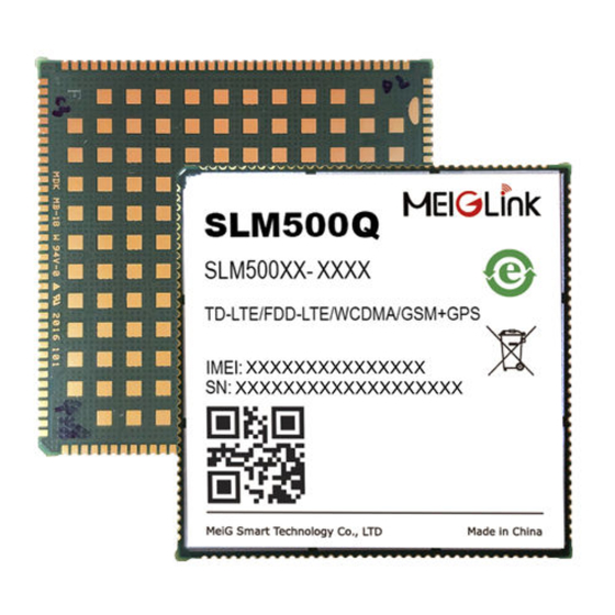
MeiG Smart product technical information 7. Production 7.1. Top And Bottom Views Of The Module Figure 48: Module top and bottom views SLM500 Hardware Design Guide Page 68... -
Page 69: Recommended Soldering Furnace Temperature Curve
Figure 49: Module recommended soldering furnace temperature curve 7.3. Humidity Sensitivity (MSL) The SLM500 module meets moisture sensitivity level 3. The dry package is subjected to the J-STD-020C specification in accordance with the IPC/JEDEC standard under ambient conditions of temperature <30 degrees and relative humidity <60%. Under ambient conditions of temperature <40 degrees and relative humidity <90%, the shelf life is at least 6... -
Page 70: Baking Requirements
The SLM500 should be baked for 192 hours in a cryogenic vessel at 40°C +5°C/- 0°C and a relative humidity of less than 5%, or in a high temperature vessel at 80°C±5°C.Bake for 72 hours. -
Page 71: Support Peripheral Device List
MeiG Smart product technical information 8. Support Peripheral Device List Table 8.1: List of supported display models Vendor Drive IC Specification ILITEK ILI9881P 1280x720 Table 8.2: Support for Camera Model List Vendor Drive IC Specification Sunny optical S5K3M2XX Sunny optical... -
Page 72: Appendix
MeiG Smart product technical information 9. Appendix 9.1. Related Documents Table 9.1: Related documents Serial numb File name Comment Digital cellular telecommunications (Phase 2+); AT command set for GSM GSM 07.07: Mobile Equipment (ME) GSM 07.10: Support GSM 07.10 multiplexing protocol Digital cellular telecommunications(Phase 2+);... - Page 73 This exterior label can use wording such as the following: “Contains FCC ID: 2APJ4-SLM500” and “Contains IC: 23860-SLM500” Changes or modifications not expressly approved by the party responsible for compliance could void the user's authority to operate the equipment.
- Page 74 MeiG Smart product technical information Please take attention that changes or modification not expressly approved by the party responsible for compliance could void the user’s authority to operate the equipment. This device complies with Part 15 of the FCC Rules. Operation is subject to the following two conditions:...
- Page 75 MeiG Smart product technical information (ii) le gain d'antenne maximal autorisé pour les appareils dans les bandes 5250-5350 MHz et 5470-5725 MHz doivent respecter le pire limiter; et (iii) le gain d'antenne maximal autorisé pour les appareils dans la bande 5725-5825 MHz doivent respecter le pire limites spé...
- Page 76 This exterior label can use wording such as the following: “Contains FCC ID: 2APJ4-SLM500” and “Contains IC: 23860-SLM500” any similar wording that expresses the same meaning may be used.
-
Page 77: Multiplexing Function
Pay attention to the following safety precautions when using or repairing any terminal or mobile phone that contains modules. The user should be informed of the following safety information on the terminal device. Otherwise, Meig will not be responsible for any consequences caused by the user not following these warning actions. - Page 78 MeiG Smart product technical information Table 9.4: Security Warnings Identification Claim When you are at a hospital or medical facility, observe the restrictions on using your phone. If necessary, please turn off the terminal or mobile phone, otherwise the medical device may malfunction due to radio frequency interference.
Need help?
Do you have a question about the SLM500 and is the answer not in the manual?
Questions and answers