
Subscribe to Our Youtube Channel
Related Manuals for NXP Semiconductors SAFE ASSURE FRDMGD3100HBIEVM


Summary of Contents for NXP Semiconductors SAFE ASSURE FRDMGD3100HBIEVM
-
Page 1: Frdmgd3100Hbievm
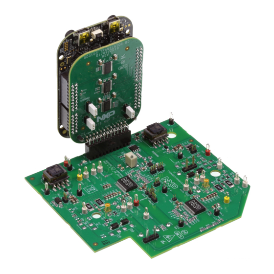
UM11134 FRDMGD3100HBIEVM half-bridge evaluation board Rev. 3 — 10 February 2020 User guide FRDMGD3100HBIEVM Figure 1. FRDMGD3100HBIEVM... -
Page 2: Important Notice
UM11134 NXP Semiconductors FRDMGD3100HBIEVM half-bridge evaluation board Important notice NXP provides the enclosed product(s) under the following conditions: This evaluation kit is intended for use of ENGINEERING DEVELOPMENT OR EVALUATION PURPOSES ONLY. It is provided as a sample IC pre-soldered to a printed circuit board to make it easier to access inputs, outputs, and supply terminals. -
Page 3: Getting Started
UM11134 NXP Semiconductors FRDMGD3100HBIEVM half-bridge evaluation board Getting started The NXP analog product development boards provide an easy-to-use platform for evaluating NXP products. These development boards support a range of analog, mixed- signal, and power solutions. These boards incorporate monolithic integrated circuits and system-in-package devices that use proven high-volume technology. -
Page 4: System Requirements
UM11134 NXP Semiconductors FRDMGD3100HBIEVM half-bridge evaluation board • TEK MSO 4054 500 MHz 2.5 GS/s 4-channel oscilloscope • Rogowski coil, PEM Model CWT Mini HF60R or CTW Mini HF30 (smaller diameter) • Two isolated high voltage probes (CAL Test Electric CT2593-1, LeCroy AP030) •... -
Page 5: Device Features
UM11134 NXP Semiconductors FRDMGD3100HBIEVM half-bridge evaluation board 4.3 Device features Table 1. Device features Device Description Features GD3100 The GD3100 is an advanced • Compliant with ASIL C/D ISO 26262 functional single channel gate driver for safety requirements IGBTs. • SPI interface for safety monitoring, programmability and flexibility •... -
Page 6: Low-Voltage Logic And Controls Connector
UM11134 NXP Semiconductors FRDMGD3100HBIEVM half-bridge evaluation board Figure 2. Connecting FRDM-KL25Z, GD3100 half-bridge EVB and translator board 4.4.1 Low-voltage logic and controls connector Low-voltage domain is 12 V VSUP/VPWR domain that interfaces with the MCU and GD3100 control registers through the 24-pin connector interface. - Page 7 UM11134 NXP Semiconductors FRDMGD3100HBIEVM half-bridge evaluation board Figure 3. Evaluation board voltage and interface domains Table 2. Low-voltage (LV) domain 24-pin connector definitions Name Function AOUTL Duty cycle encoded signal (low-side) n.c. No connection CSBL Chip select bar (low-side) n.c. No connection...
-
Page 8: Test Point Definitions
UM11134 NXP Semiconductors FRDMGD3100HBIEVM half-bridge evaluation board Name Function AOUTH Duty cycle encoded signal (high-side) PWMH PWM input (high-side) FSSTATEH Fail-safe state (high-side) Ground INTBH Interrupt bar (high-side) 4.4.2 Test point definitions All test points are clearly marked on the evaluation board. - Page 9 UM11134 NXP Semiconductors FRDMGD3100HBIEVM half-bridge evaluation board Test point Reference Definition designator VRFL TP18 Monitor internal 5.0 V reference for analog circuitry on HV isolated TSENSEL TP19 Input for low-side IGBT temperature measurement. Onboard components optimized for use with NTC.
-
Page 10: Power Related Jumpers Configuration
UM11134 NXP Semiconductors FRDMGD3100HBIEVM half-bridge evaluation board 4.4.3 Power related jumpers configuration Figure 5. Power supply and jumpers configuration Table 4. Power related jumper definitions Jumper Reference Position Function designator VDDL Open VDD-VSUP are separate. Device powered from VSUP, VDD uses internal regulator (default) Closed VDD-VSUP connected. -
Page 11: Configuring Power Delivery To Gd3100
UM11134 NXP Semiconductors FRDMGD3100HBIEVM half-bridge evaluation board Jumper Reference Position Function designator VEEH_SEL VEE is negative supply (default) VEE is tied to IGBT emitter (GNDISOH) Open Not allowed. VCC and VEE float relative to IGBT emitter (GNDISOH) The FRDMGD3100HBIEVM provides configurability for different gate driver power architectures. -
Page 12: Signal Related Jumpers And Configuration
UM11134 NXP Semiconductors FRDMGD3100HBIEVM half-bridge evaluation board 4.4.4 Signal related jumpers and configuration Figure 6. Signal related jumper locations Table 5. Signal related jumper configurations Jumper Reference Position Function designator PS_EN MCU/software controls VCC/VEE power supply VCC/VEE power supplies always enabled. MCU control signal is disconnected (default). -
Page 13: Spi Configuration Options
UM11134 NXP Semiconductors FRDMGD3100HBIEVM half-bridge evaluation board Jumper Reference Position Function designator PWMLSEL PWMALTL receives complementary PWMH signal. Enables dead time protection (default). PWMALTL is grounded. Bypasses dead time control (i.e. double-pulse, short-circuit test). Open Not allowed. PWMALTL is in an unknown state. -
Page 14: Bottom View
UM11134 NXP Semiconductors FRDMGD3100HBIEVM half-bridge evaluation board Allow control to turn VCC/VEE flyback supplies ON/OFF: • Connect PS_EN (J25) jumper to 1-2 • Utilize EN_PS signal (J5.10) to enable or disable the power supplies 4.4.5 Bottom view Figure 7. GD3100 evaluation board bottom view 4.4.6 Gate drive resistors... -
Page 15: Led Interrupt Indicators
UM11134 NXP Semiconductors FRDMGD3100HBIEVM half-bridge evaluation board Figure 8. Gate drive resistors 4.4.7 LED interrupt indicators Interrupt LEDs are provided to visually alert the user of a reported fault. The LEDs are supplied with 3.3 V from the KL25Z, and are driven directly by the INTB pin of the respective GD3100 device. -
Page 16: Kinetis Kl25Z Freedom Board
UM11134 NXP Semiconductors FRDMGD3100HBIEVM half-bridge evaluation board Figure 9. LED interrupt indicators Table 6. Interrupt LED definitions Reference Description designator Low-side INTB Connected to the INTB output pin (active low) of low-side GD3100 • LED is ON: indicates reported fault, check system •... -
Page 17: Logic Translator Board
UM11134 NXP Semiconductors FRDMGD3100HBIEVM half-bridge evaluation board Figure 10. Freedom Development Platform 4.6 Logic translator board The FRDMGD3100HBIEVM includes a logic translator board, which provides simple isolation and is capable of level-shifting communication signals between the MCU and the GD3100 driver board. The driver board is exposed to high voltage, and may require 3.3 V or 5.0 V logic, necessitating an interface board. -
Page 18: Configuring The Translator For Kl25Z-Controlled Pwm
UM11134 NXP Semiconductors FRDMGD3100HBIEVM half-bridge evaluation board Table 7. Translator board jumper functionality Jumper Reference Position Function designator VCCSEL J233 5.0 V regulator from KL25Z powers all translator VCC, 5.0 V signals to/from the driver board (default) • Use with 5.0 V GD3100 (MC33GD3100EK) 3.3 V regulator from KL25Z powers all translator VCC,... -
Page 19: Configuring The Translator For External Pwm Control
UM11134 NXP Semiconductors FRDMGD3100HBIEVM half-bridge evaluation board 4.6.2 Configuring the translator for external PWM control The translator may be setup to pass externally provided signals to the driver board, normally applied at EXT_PWML (TP10) and EXT_PWMH (TP11) test points. These signals do not pass through the translator, so their logic level must match those required by the GD3100 populated on the driver board. -
Page 20: Quick Start
UM11134 NXP Semiconductors FRDMGD3100HBIEVM half-bridge evaluation board • Voltmeter for monitoring high voltage DC Link supply • Load coil for double pulse and short-circuit type 2 testing Figure 12. Evaluation board and system setup 5.2 Quick start 5.2.1 Scope and purpose This section provides comprehensive quick start notes for the FRDMGD3100HBIEVM half-bridge evaluation kit. -
Page 21: Installation And Use Of Software Tools
UM11134 NXP Semiconductors FRDMGD3100HBIEVM half-bridge evaluation board b. For alternate configurations and setup details, see Section 4.4.3, Section 4.4.4 "Signal related jumpers and configuration", and Section 4.4.7 "LED interrupt indicators". 4. Start SPIGEN application software on PC. Connect USB cable from PC to USBKL25Z port on KL25Z micro board. -
Page 22: Installing Spigen On Your Computer
UM11134 NXP Semiconductors FRDMGD3100HBIEVM half-bridge evaluation board Figure 13. FRDM-KL25Z setup and interface 6.1 Installing SPIGen on your computer The latest version of SPIGen supports the GD3100 and is designed to run on any Windows 10, Windows 8, or Windows 7-based operating system. To install the software, do the following: 1. -
Page 23: Using The Spigen Graphical User Interface
UM11134 NXP Semiconductors FRDMGD3100HBIEVM half-bridge evaluation board 4. Find the most recent MDS-DEBUG-FRDM-KL25Z_Pemicro_v***.SDA and copy/drag- and-drop into the BOOTLOADER device. 5. Reboot the board by unplugging and re-plugging the connection to the OpenSDA port. Verify now the device appears as a “KL25Z” device to continue. -
Page 24: Mode Registers
UM11134 NXP Semiconductors FRDMGD3100HBIEVM half-bridge evaluation board Figure 14. SPIGen general view Some general guidelines on SPIGen usage: • When attempting to change operating modes, configuration registers, or status mask bits, ensure the CONFIG_EN bit in the MODE2 register is set to 1. Fault status bits can be cleared without CONFIG_EN being set to 1. -
Page 25: Configuration Register
UM11134 NXP Semiconductors FRDMGD3100HBIEVM half-bridge evaluation board Figure 15. Mode registers and GPIO controls view 6.3.2 Configuration register See GD3100 data sheet for configuration SPI register descriptions. When attempting to change configuration parameters, ensure the CONFIG_EN bit in the MODE2 register is set to 1. READ operations send identical back-to-back commands so the response is obtained upon a single click of the Read button. -
Page 26: Status And Mask Register
UM11134 NXP Semiconductors FRDMGD3100HBIEVM half-bridge evaluation board 6.3.3 Status and mask register See GD3100 data sheet for status and mask SPI register descriptions. INTB indicators mirror the status of the INTB pin on both high-side and low-side GD3100 simultaneously, but only one (either high-side or low-side) can be read at a time over SPI (selected by “SPI 0”... -
Page 27: Pulse Test
UM11134 NXP Semiconductors FRDMGD3100HBIEVM half-bridge evaluation board 6.3.4 Pulse test The Pulse test view allows a few simple waveforms to be applied to the PWM and PWMALT pins, to evaluate with an IGBT. For double pulse test, short-circuit test, and short-circuit test 2, it is recommended to bypass dead time protection, as described in Section 4.4.4.2 "Configuring dead time... -
Page 28: Single Command
UM11134 NXP Semiconductors FRDMGD3100HBIEVM half-bridge evaluation board 6.3.6 Single command The Single command view contains a log of recent commands, displayed in hexadecimal format. Single SPI commands can be saved and recalled by name. Commands defined here are available for scripting in the Batch commands page. SPI words sent and received (initiated from any tab) are logged here in hexadecimal and can be saved and exported in a text file. - Page 29 UM11134 NXP Semiconductors FRDMGD3100HBIEVM half-bridge evaluation board Figure 21. Batch commands view 6.4 Troubleshooting Some common issues and troubleshooting procedures are detailed below. This is not an exhaustive list by any means, and additional debug may be needed: Problem Evaluation Explanation...
- Page 30 UM11134 NXP Semiconductors FRDMGD3100HBIEVM half-bridge evaluation board Problem Evaluation Explanation Corrective action(s) PWM output is good, but with Check for dead time fault (DTFLT) in Dead time is enforced, but fault Clear DTFLT fault bit (STATUS2). persistent fault reported STATUS2 register...
- Page 31 UM11134 NXP Semiconductors FRDMGD3100HBIEVM half-bridge evaluation board Problem Evaluation Explanation Corrective action(s) VCCOV fault reported on startup Check position of VEEx_SEL (J1, J2) VEEx_SEL jumpers set the VCC/VEE Disable HV domain power supplies, jumpers potential relative to each HV domain and set correct VEExSEL jumpers.
- Page 32 UM11134 NXP Semiconductors FRDMGD3100HBIEVM half-bridge evaluation board Revision history Revision history Revision Date Description 20180702 Initial version 20190403 • Section 4: complete rewrite • Global: various figures, tables updated to support new driver board revision (B) • Global: various figures, tables updated to support new translator board revision (C) •...
- Page 33 NXP Semiconductors and its suppliers accept no liability for inclusion and/or use of NXP Semiconductors products in such equipment or 10.2 Disclaimers applications and therefore such inclusion and/or use is at the customer's own risk.
- Page 34 UM11134 NXP Semiconductors FRDMGD3100HBIEVM half-bridge evaluation board Tables Tab. 1. Device features ..........5 Tab. 5. Signal related jumper configurations ....12 Tab. 2. Low-voltage (LV) domain 24-pin connector Tab. 6. Interrupt LED definitions ........16 definitions ............7 Tab. 7.
-
Page 35: Table Of Contents
UM11134 NXP Semiconductors FRDMGD3100HBIEVM half-bridge evaluation board Contents FRDMGD3100HBIEVM .........1 Troubleshooting ..........29 Important notice ..........2 Schematics, board layout and bill of Getting started ............ 3 materials .............31 Kit contents/packing list ........3 References ............31 Required equipment .......... 3 Revision history ..........
Need help?
Do you have a question about the SAFE ASSURE FRDMGD3100HBIEVM and is the answer not in the manual?
Questions and answers