Advertisement
Test Procedure for NCP571 0V9 DFN6 LDO Demoboard
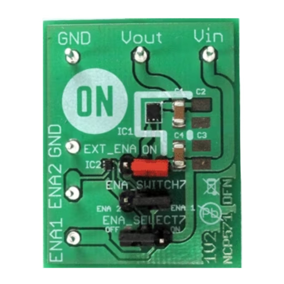
1. Enable pin connected to Vin
1.Check the position of jumper and correct it if necesary.
a)EXT_ENA
b)ENA_SELECT
c)POWER ENA2
2. Connect the test setup as shown Figure 1
3. Appy an input voltage Vin = 2.7 V
4. Appy Iout = 0mA load.
5. Check that Vout is 0.9 V.
6. Increase Iout up to 150 mA
7. Increase Vin up to 12 V and decrease the load in accordance with SOA
8. Power down the Load
9. Power down the Vcc
10. End of test
07/29/2010
- ON
- ENA1 or ENA2
- OFF
1
www.onsemi.com
Advertisement
Table of Contents

Subscribe to Our Youtube Channel
Related Manuals for ON Semiconductor NCP571 0V9 DFN6 LDO


Summary of Contents for ON Semiconductor NCP571 0V9 DFN6 LDO
- Page 1 Test Procedure for NCP571 0V9 DFN6 LDO Demoboard 1. Enable pin connected to Vin 1.Check the position of jumper and correct it if necesary. a)EXT_ENA - ON b)ENA_SELECT - ENA1 or ENA2 c)POWER ENA2 - OFF 2. Connect the test setup as shown Figure 1 3.
- Page 2 2. Enable pin connected to pin ENA1 1.Check the position of jumper and correct it if necesary. a)EXT_ENA - EXT_ENA b)ENA_SELECT - ENA1 c)POWER ENA2 - OFF 2. Connect the test setup as shown Figure 1 3. Appy an input voltage Vin = 2.7 V 4.
Need help?
Do you have a question about the NCP571 0V9 DFN6 LDO and is the answer not in the manual?
Questions and answers