Table of Contents
Advertisement
Quick Links
Advertisement
Table of Contents

Subscribe to Our Youtube Channel
Related Manuals for Cimon CM3-SP32PWM


Summary of Contents for Cimon CM3-SP32PWM
- Page 3 Before You Start This manual contains important information on the use and operation of this device. Please read all the information carefully for optimal performance and to prevent any damage or misuse of the device. Safety symbols are classified into two categories, “WARNING” and “CAUTION”. Warning This symbol describes situations that could cause major or fatal injury to the user.
- Page 4 Design Precautions ( Warning) Please install a safety circuit to protect entire control system in case of an unexpected power shut-down and PLC module malfunction. Such anomalies may severely compromise the integrity of the overall system. External to the PLC, please install circuits and switches to safeguard the system from mechanical damages (ex.
- Page 5 Precautions for mounting ( Caution) Use the PLC in the environment that meets the general specifications given in this manual. Using this PLC in any environment outside the range of the general specifications could result in electric shock, fire, malfunction, or damage to or deterioration of the product.
- Page 6 Precautions for test run and repair ( Warning) Please do not touch the terminals when the power is ON. Doing so could cause an electric shock or malfunctions. When cleaning or tightening the screw, turn off the power of PLC and all other systems.
-
Page 7: Table Of Contents
PWM Output Module User’s manual CONTENTS Introduction ....................2 Features ..........................4 Design and Dimensions ..................... 5 Configuring terminal blocks and names ................6 Specification ....................7 General specification ......................7 I/O Specification ........................ 8 Data Memory ....................9 I/O Memory ........................9 3.1.1 Output area ........................ -
Page 8: Introduction
1 Introduction This manual will guide the reader through installation, functions, safety use and operation of the PWM output module (CM3-SP32PWM) of the PLC-S. This manual will need to be read and understood before attempting to install or use the device. - Page 9 PWM Output Module User’s manual Run the CICON and make a connection with PLC. Click the [Online] – [About PLC information] or the icon below. You can check the version of CPU firmware in the dialog box. [Figure 2] Route to check CPU firmware Total Solution for Industrial Automation...
-
Page 10: Features
PWM (Pulse-Width Modulation) is a digital output that can be used as an analog output by controlling the duty cycle that contains a certain frequency. CIMON PWM Output Module has a pulse output function added onto the general digital output, so it has the same specifications as a CM3-SP32EOC when used as a general digital output. -
Page 11: Design And Dimensions
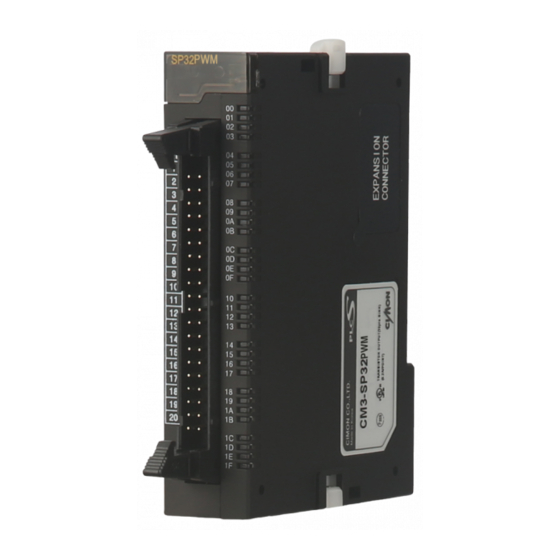
PWM Output Module User’s manual 1.2 Design and Dimensions [Figure 3] PWM module appearance Total Solution for Industrial Automation... -
Page 12: Configuring Terminal Blocks And Names
CH 1. Introduction 1.3 Configuring terminal blocks and names For long cables, there is a potential for unintended distortion of the PWM pulse. Therefore, 1.0M cable is strongly recommended. Each DC12/24V and DC GND are connected to the corresponding terminal internally. -
Page 13: Specification
Impression time : 11ms Inner Impact IEC61131-2 Pulse wave : a sine half-wave pulse (3 times for each direction ±X, ±Y, ±Z, total on 3 times) Square wave impulse CIMON Internal ±2kV(10 minutes) noise Test Standard Electromagnetism IEC61131-2 Voltage : 4kV(Contact Discharge) -
Page 14: I/O Specification
CH 2. Specification 2.2 I/O Specification Types Specifications of item Rated input/output voltage DC 12V ~ 24V Response time ≤1ms Operating indicator LED lighting when the power ON Insulation for anticorrosion Photocoupler Input method Output method Source External connection circuit Internal circuit [Table 2] I/O Specification of PWM module Total Solution for Industrial Automation... -
Page 15: Data Memory
PWM Output Module User’s manual 3 Data Memory Data memory is largely classified into two categories: I/O memory and buffer memory. I/O memory exchanges I/O data with the CPU through the X and Y area. Buffer memory exchanges user data with data areas in CPU module using FROM∙ FROMP/TO∙TOP instruction. - Page 16 CH 3. Data Memory Signal Direction : CPU → PWM Output Module Input Signal Name Output Signal Name General output General output General output General output Frequency A, CH1, PWM output Frequency C, CH9, PWM output (or a general output) (or a general output) Frequency A, CH2, PWM output Frequency C, CH10, PWM output...
-
Page 17: Buffer Memory
PWM Output Module User’s manual 3.2 Buffer Memory The PWM output module is equipped with shared memories inside to exchange the data with CPU. One of these is called buffer memory, which is a collection of word (16Bit)-unit data. This buffer memory is readable and configurable on scan program, using FROM∙FROMP/TO∙TOP instructions. - Page 18 CH 3. Data Memory Set-up value Initial OFFSET Item Access parameter value CH11 duty cycle ratio 0~1000 Ex) When duty cycle ratio is set to 100, 100 x 0.1% (x 0.1%) = 10.0% CH12 duty cycle ratio 0~1000 Available Later CH1 duty cycle ramp time(x10ms) 0~65535 Ex) When Frequency ramp control time is set to 100,...
-
Page 19: Functions
As illustrated above, the PWM controls the output from minimum to maximum values by changing the duty cycle of the pulse. CIMON PWM output module can be either general digital output or PWM output. The general digital output can be used up to 32-pin points. From these 32-pin points, a total of 12-pin points support PWM output. -
Page 20: Enable Of Pwm Output (Buffer Memory Offset 0)
CH 4. Functions 4.1 Enable of PWM output (Buffer Memory Offset 0) When PWM-capable points’ BIT value is set to 0, it will be possible to use them as general output points. Similarly, if it is set to 1, it will be operated as PWM output. The PWM output function can be enabled by using TO instruction in the buffer memory Offset 0. -
Page 21: Controlling Frequency (Buffer Memory Offset 1 ~ 3)
PWM Output Module User’s manual 4.2 Controlling frequency (Buffer Memory Offset 1 ~ 3) The PWM can control the range of frequency from 0pps to 4000pps, and 4 channels per group for a total of 3 groups. The frequencies of each group are set by TO instruction at OFFSET 1~3 area of buffer memory. -
Page 22: Controlling Duty Cycle (Pwm) (Buffer Memory Offset 10 ~ 21)
CH 4. Functions 4.3 Controlling duty cycle (PWM) (Buffer Memory Offset 10 ~ 21) The PWM provides functions to control the duty cycle from 0.0% to 100.0% with a 1/1000 resolution. Duty cycles can be controlled by a channel, for a maximum of 12 channels. -
Page 23: Frequency Ramp Control (Buffer Memory Offset 5 ~ 7)
PWM Output Module User’s manual 4.4.1 Frequency ramp control (Buffer memory Offset 5 ~ 7) If frequency ramp control time is configured prior to a change in frequency value, any change in pulse frequency will be applied gradually. Frequency ramp control time can be operated by using TO instruction on buffer memory Offset 5 ~ 7. -
Page 24: Duty Cycle Ramp Control (Buffer Memory Offset 30 ~ 41)
CH 4. Functions 4.4.2 Duty cycle ramp control (Buffer memory Offset 30 ~ 41) If duty cycle ramp control time is configured prior to setting a duty cycle value, any change in the duty cycle will be applied gradually. The duty cycle ramp control can be operated by using TO instruction on buffer memory Offset 30~41. -
Page 25: Operating The Pwm Output Module
PWM Output Module User’s manual 5 Operating the PWM Output Module Through examples, this chapter outlines a method to configure a program using the PWM output module. In order to use the ramp control time as intended, please set up the ramp control time prior to inputting frequency or duty cycle values. - Page 26 CH 5. Operating the PWM Output Module Entire scan program is as below. (1) Use TOP instruction to enter value 2 on buffer memory Offset 0 to enable channel PWM output. (2) Receive the M00 value and trigger the function. Enter 1000 on buffer memory Offset 1, 500 on Offset 5 and 500 on Offset 11 by using TOP instruction so they can be changed 0pps to 1000pps for 5 seconds with a duty cycle of 50.0%.
-
Page 27: Practical Examples
PWM Output Module User’s manual 5.2 Practical Examples The following are examples about how to utilize PWM output module. Example 1 is about motor control using frequency ramp control function. Example 2 is about PID temperature control using frequency ramp control function and duty cycle. Example 1: Softstart Using Ramp Control This is an example to control an escalator using stepping motor control. - Page 28 CH 5. Operating the PWM Output Module (1) Initialize module parameter as below. Enable CH2 PWM (Buffer memory Offset 0) Initial frequency 0pps (Buffer memory Offset 1), frequency ramp control time 3 seconds(Buffer memory Offset 5). Duty cycle 50.0% (Buffer memory Offset 11), No duty cycle ramp control ...
- Page 29 PWM Output Module User’s manual Example 2: PWM PID Control This is an example about PID temperature control of the heater which turns on at 24V and turns off on at 0V. Basic requirement of the system is as below. <Requirements>...
- Page 30 CH 5. Operating the PWM Output Module (2) Set proper Kp, Ki, Kd value and set sampling cycle to 1 second. (3) Enable PWM output of CH2 to write value 2 to buffer memory Offset 0 by using TOP instruction. (4) Set frequency and frequency ramp control time.
- Page 31 PWM Output Module User’s manual (7) Scale transform the MV value(D102) by using SCL instruction and save the value to D200. Set the duty cycle by using configured D200 value. Set D200 value to buffer memory Offset 11 by using TOP instruction. Total Solution for Industrial Automation...
-
Page 32: Maintenance Work And Repair
CH 6. Maintenance work and Repair 6 Maintenance work and repair It is recommended to have the PLC checked and diagnosed regularly to maintain its ideal performance. The following describes what is to be done in a maintenance work. 6.1 Maintenance work ... -
Page 33: Repair
PWM Output Module User’s manual 6.2 Repair Replacing a module If a module requires replacement due to damage or failure, the following procedure should be followed. Turn the PLC drive power supply off. Isolate the connector from PLC-S. Remove Din rail fixing hook and remove the PLC. Release PLC-S fixing hook and remove/replace the module. -
Page 34: Trouble Shooting
CH 6. Maintenance work and Repair 6.3 Trouble shooting This section describes errors that may happen during run-time and actions to be taken. See the following items before making a judgement on PLC problems. (1) Check if the power is on. (Does PLC drive input voltage enabled normally?) (2) Check that each module is mounted (such as power supply, CPU, I/O, special modules) or wired (Such as I/O signal, cable) properly. -
Page 35: Appendix 1 Using From∙Fromp/To∙Top Instructions
PWM Output Module User’s manual Appendix 1 Using FROM∙FROMP/TO∙TOP Instructions The CIMON PLC is composed of various special modules such as AD, DA, High Speed Counter, etc. All of these have a shared memory in their hardware for data exchange with CPU module. - Page 36 Appendix 1. Using FROM∙FROMP/TO∙TOP Instructions (1) S1 (base and slot number) CIMON PLC can be expanded up to 16 bases. Following is a sample drawing of 16 bases expansion. [Figure 10] Example of PLC-CM1 Series module extension The first operand of FROM / FROMP instruction must be base and slot numbers. The upper Byte is assigned as base number and the lower Byte is assigned as slot number, so can be easily understood with hexa-decimal notation.
- Page 37 PWM Output Module User’s manual [Figure 11] Example of PLC-S Series module extension In the PLC-S series, H00 is used for upper Byte as there is no base expansion. (2) S2 (Start address of buffer memory) Designate the start address of buffer memory to read. Please refer to the manual or quick-reference guide of objective module.
- Page 38 Appendix 1. Using FROM∙FROMP/TO∙TOP Instructions Example 1: How To Use FROM/FROMP Instruction The following is an example program which reads one word and eight words. It assumes the special module is CM1-ADxxxx and installed in fourth slot of the first expanded base.
- Page 39 PWM Output Module User’s manual 2. TO/TOP instruction ‘TO/TOP’ instruction writes word data to shared memory of special module such as DA modules. The typical usage of the instruction can be represented by following [Figure 12] How to TO/TOP instruction Form Content Note...
- Page 40 Appendix 1. Using FROM∙FROMP/TO∙TOP Instructions (4) Number of words to write Designate the number of words to write. Example 2: How To Use TO/TOP Instruction The following is an example program which writes one word and eight words. It assumes the special module is CM1-DAxxxx and installed in fourth slot of the first expanded base.
-
Page 41: Appendix 2 Method Of Address Allocation
PWM Output Module User’s manual Appendix 2 Method of Address Allocation 1. Address Allocation [Figure 13] Notation of each Bit/Word device (1) Bit Data Designation Composition [Device Symbol] + [Card No.] + [Bit No.] Device Symbol X, Y, M, K, L, F Card No. - Page 42 Appendix 2. Method of Address Allocation 2. I/O Address Allocation I/O Address Allocation is to assign each modules a number to output the data from the input module. I/O Address is allocated in order of expanded base access from the local base. Address number is allocated from left side excluding the power of each bases and CPU.
- Page 43 PWM Output Module User’s manual (1) 8-pin I/O Module Composition: POWER + CPU + 16-pin Input Module + 16-pin Output Module + 8-pin Input Module + 8-pin Output Module +16-pin Input Module [Figure 15] Example of CM1-Series Module Composition (8-pin I/O Module) Total Solution for Industrial Automation...
- Page 44 Appendix 2. Method of Address Allocation (2) 32-pin I/O Module 16-pin Module takes 1 slot and 32-pin Module takes 2 slots. Composition: POWER + CPU +16-pin Input Module + 16-pin Output Module + 32-pin Input Module + 32-pin Output Module + 16-pin Input Module [Figure 16] Example of CM1-Series Module Composition (32-pin I/O Module) Total Solution for Industrial Automation...
- Page 45 PWM Output Module User’s manual Address of Expanded Base is connected after the Address of Local Base. [Figure 17] Case of Additional CM1-Series Connection In case of PLC-S CPU, it has an I/O function unlike the CM1-Series I/O address allocation. Address number is assigned in order from CPU. PLC-S CPU is separated into CM3-SP32MDTx and CM3-SP16MDRx.
- Page 46 Appendix 2. Method of Address Allocation Composition: CPU 32pin + 32-pin Input Module +32-pin Output Module + 16-pin I/O Module +16-pin I/O Module + Output 16pin + Analog Module 16pin + Communication Module 16pin [Figure 18] Example of PLC-S Series Module composition Total Solution for Industrial Automation...
- Page 47 PWM Output Module User’s manual 3. X/Y I/O area allocation (1) X area (Bit / Output device) This is an Input pin which receives a signal from Input Card. This is a read-only device which user cannot input the value randomly. X area is Bit Type. It means that the size of detailed table signifies the number of Bit.
- Page 48 Appendix 2. Method of Address Allocation 4. Features I/O X, Y respond to external devices. X is to receive the signal of input device such as Push button switch, Limit switch and etc. Y is to convey the calculation results from Output Device such as Solenoid Valve, Motor, Lamp and etc.
-
Page 49: Index
PWM Output Module User’s manual INDEX [ Figure Reference List ] [Figure 1] Route to check software version ∙∙∙∙∙∙∙∙∙∙∙∙∙∙∙∙∙∙∙∙∙∙∙∙∙∙∙∙∙∙∙∙∙∙∙∙∙∙∙∙∙∙∙∙∙∙∙∙∙∙∙∙∙∙∙∙∙∙∙∙∙∙∙∙∙∙∙∙∙∙∙∙∙∙∙∙∙∙∙∙∙∙∙∙∙∙∙ 2p [Figure 2] Route to check CPU firmware ∙∙∙∙∙∙∙∙∙∙∙∙∙∙∙∙∙∙∙∙∙∙∙∙∙∙∙∙∙∙∙∙∙∙∙∙∙∙∙∙∙∙∙∙∙∙∙∙∙∙∙∙∙∙∙∙∙∙∙∙∙∙∙∙∙∙∙∙∙∙∙∙∙∙∙∙∙∙∙∙∙∙∙∙∙∙∙∙∙∙∙ 3p [Figure 3] PWM module appearance ∙∙∙∙∙∙∙∙∙∙∙∙∙∙∙∙∙∙∙∙∙∙∙∙∙∙∙∙∙∙∙∙∙∙∙∙∙∙∙∙∙∙∙∙∙∙∙∙∙∙∙∙∙∙∙∙∙∙∙∙∙∙∙∙∙∙∙∙∙∙∙∙∙∙∙∙∙∙∙∙∙∙∙∙∙∙∙∙∙∙∙∙∙∙∙∙∙ 5p [Figure 4] Arrangement of terminals and its notations ∙∙∙∙∙∙∙∙∙∙∙∙∙∙∙∙∙∙∙∙∙∙∙∙∙∙∙∙∙∙∙∙∙∙∙∙∙∙∙∙∙∙∙∙∙∙∙∙∙∙∙∙∙∙∙∙∙∙∙∙∙∙∙∙∙∙∙∙∙∙∙ 6p [Figure 5] Data exchange between PWM module and CPU ∙∙∙∙∙∙∙∙∙∙∙∙∙∙∙∙∙∙∙∙∙∙∙∙∙∙∙∙∙∙∙∙∙∙∙∙∙∙∙∙∙∙∙∙∙∙∙∙∙∙∙∙∙∙∙∙∙∙∙∙∙∙∙... - Page 50 Index [ Table Reference List ] [Table 1] General specification of PWM module ∙∙∙∙∙∙∙∙∙∙∙∙∙∙∙∙∙∙∙∙∙∙∙∙∙∙∙∙∙∙∙∙∙∙∙∙∙∙∙∙∙∙∙∙∙∙∙∙∙∙∙∙∙∙∙∙∙∙∙∙∙∙∙∙∙∙∙∙∙∙∙∙∙∙∙∙∙∙∙∙ 7p [Table 2] I/O Specification of PWM module ∙∙∙∙∙∙∙∙∙∙∙∙∙∙∙∙∙∙∙∙∙∙∙∙∙∙∙∙∙∙∙∙∙∙∙∙∙∙∙∙∙∙∙∙∙∙∙∙∙∙∙∙∙∙∙∙∙∙∙∙∙∙∙∙∙∙∙∙∙∙∙∙∙∙∙∙∙∙∙∙∙∙∙∙∙∙ 8p [Table 3] Usage of each pin of PWM module ∙∙∙∙∙∙∙∙∙∙∙∙∙∙∙∙∙∙∙∙∙∙∙∙∙∙∙∙∙∙∙∙∙∙∙∙∙∙∙∙∙∙∙∙∙∙∙∙∙∙∙∙∙∙∙∙∙∙∙∙∙∙∙∙∙∙∙∙∙∙∙∙∙∙∙∙∙∙∙∙∙∙ 10p [Table 4] Usage and meaning of each buffer memory (PWM module) ∙∙∙∙∙∙∙∙∙∙∙∙∙∙∙∙∙∙∙∙∙∙∙∙∙∙∙∙∙∙∙∙∙∙∙∙∙∙∙∙∙∙∙∙∙∙∙ 11p [Table 5] Available point of PWM output ∙∙∙∙∙∙∙∙∙∙∙∙∙∙∙∙∙∙∙∙∙∙∙∙∙∙∙∙∙∙∙∙∙∙∙∙∙∙∙∙∙∙∙∙∙∙∙∙∙∙∙∙∙∙∙∙∙∙∙∙∙∙∙∙∙∙∙∙∙∙∙∙∙∙∙∙∙∙∙∙∙∙∙∙∙∙∙∙...
- Page 51 PWM Output Module User’s manual Version History Released Date Version Description 22/09/2017 V1.0 First Edition Total Solution for Industrial Automation...
- Page 56 Date 22/09/17 V1.0...
Need help?
Do you have a question about the CM3-SP32PWM and is the answer not in the manual?
Questions and answers