Table of Contents
Advertisement
SERVICE MANUAL
Ver 1.4 2002. 10
US and foreign patents licensed from Dolby
Laboratories.
• OpenMG, "MagicGate", "MagicGate Memory Stick", "Memory Stick",
VAIO,MusicClip and their logos are trademarks of Sony Corporation.
• "WALKMAN" is a trademark of Sony Corporation.
• Microsoft,Windows,Windows NT and Windows Media are trademarks
or registered trademarks of Microsoft Corporation in the United States
and/or other countries.
• IBM and PC/AT are registered trademarks of International Business
Machines Corporation.
• Macintosh is a trademark of Apple Computer,Inc.in the United States
and/or other countries.
• All other trademarks are trademarks of their respective owners. ™ and
® marks are omitted in this manual.
Sony Corporation
9-873-443-05
2002J0500-1
Personal Audio Company
C 2002.10
Published by Sony Engineering Corporation
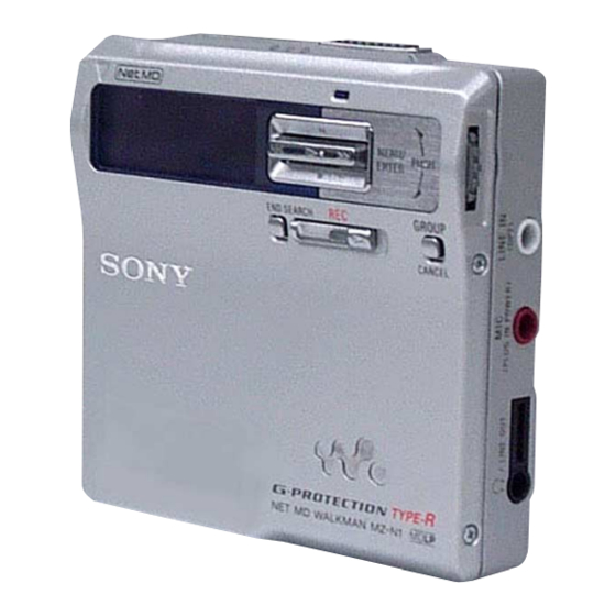
MZ-N1
Model Name Using Similar Mechanism
Mechanism Type
Optical Pick-up Name
SPECIFICATIONS
Audio playing system
MiniDisc digital audio system
Laser diode properties
Ma te rial : GaAlAs
Wavelength:
= 790 nm
Emis sion dura tion : continuous
Laser output : le ss tha n 44. 6 W
(This output is the va lue measured at a distance
of 200 mm from the lens surface on the op tica l
pick-up blo ck with 7 mm a pe rture .)
Recording and playback time (when
using MDW-80)
Ma ximum 16 0 min. in monaural
Ma ximum 32 0 min. in stereo
Revolutions
382 rpm to 2,700 rpm (CLV)
Error correction
ACIRC (Advanced Cro s s Interleave Reed
S olomo n Code )
Sampling frequency
44.1 kHz
Sampling rate converter
Input: 32 kHz/44. 1 kHz/48 kHz
Coding
ATRAC (Adaptive TRa nsform Acoustic
Coding)
ATRAC3 — LP 2/LP4
PORTABLE MINIDISC RECORDER
US Model
Canadian Model
AEP Model
UK Model
E Model
Australian Model
Chinese Model
Tourist Model
NEW
MT-MZN1-171
LCX-5R
– Continued on next page –
Advertisement
Table of Contents

Related Manuals for Sony Net MD Walkman MZ-N1


Summary of Contents for Sony Net MD Walkman MZ-N1
- Page 1 US and foreign patents licensed from Dolby Laboratories. • OpenMG, “MagicGate”, “MagicGate Memory Stick”, “Memory Stick”, VAIO,MusicClip and their logos are trademarks of Sony Corporation. • “WALKMAN” is a trademark of Sony Corporation. • Microsoft,Windows,Windows NT and Windows Media are trademarks or registered trademarks of Microsoft Corporation in the United States and/or other countries.
- Page 2 Technology Industries Association) standard. nickel Whe n us ing a 100% fully c harged metal hydride rechargeable battery (NH- 14WM(A)). Whe n us ing a Sony LR6 (S G) “STAMINA ” a lka line dry battery (pro duced in Japan) À LA SÉCURITÉ!
-
Page 3: Table Of Contents
CAUTION Use of controls or adjustments or performance of procedures other than those specified herein may result in hazardous ra- diation exposure. On power sources • Use house curre nt, nikel metal hyd ride rechargeable battery, LR6 (S G) battery, or car battery. -
Page 4: Servicing Notes
MZ-N1 Ver 1.1 NOTES ON HANDLING THE OPTICAL PICK-UP BLOCK OR BASE UNIT The laser diode in the optical pick-up block may suffer electro- static break-down because of the potential difference generated by the charged electrostatic load, etc. on clothing and the human body. -
Page 5: General
Looking at controls The recorder A END SEARCH button • Other operations B Display window Operation C VOLUME +/– buttons Press N The VOLUME + button has a tactile dot. Press . D Battery compartment Press> E T MARK button Flip towards X F HOLD switch (at the rear) Flip towards x... -
Page 6: Disassembly
MZ-N1 • This set can be disassembled in the order shown below. 3-1. DISASSEMBLY FLOW 3-2. BOTTOM PANEL ASSY (Page 7) 3-3. UPPER PANEL SECTION (Page 7) 3-5. MAIN BOARD SECTION (Page 8) 3-7. MD MECHANISM DECK (MT-MZN1-171), CHASSIS ASSY (Page 9) 3-8. -
Page 7: Bottom Panel Assy
Note: Follow the disassembly procedure in the numerical order given. 3-2. BOTTOM PANEL ASSY Note : On installation, adjust the position of both switch (S801) and knob (hold). knob (hold) 5 two screws (M1.4) 3-3. UPPER PANEL SECTION 3 two screws (M1.4) 6 upper panel section S801 1 Open the battery... -
Page 8: Lcd Module, Upper Panel Assy
MZ-N1 Ver 1.3 3-4. LCD MODULE, UPPER PANEL ASSY 3 upper panel section 3-5. MAIN BOARD SECTION 8 main board section 3 four screws (M1.4) 1 three screws (1.7) 6 flexible board (optical pick-up) (CN501) 7 holder (terminal) 4 screw 2 flexible board (motor) (CN502) (M1.4) 2 Remove the LCD module... -
Page 9: Battery Case Assy, Main Board
3-6. BATTERY CASE ASSY, MAIN BOARD 1 Remove the solder of terminal (plus). 1 Remove the solder of terminal (minus). 3-7. MD MECHANISM DECK (MT-MZN1-171), CHASSIS ASSY 2 boss 2 battery case assy 3 MD mechanism deck (MT-MZN1-171) 2 boss 1 screw (M1.4) 4 spring (POP) -
Page 10: Op Service Assy (Lcx-5R)
MZ-N1 3-8. OP SERVICE ASSY (LCX-5R) 1 washer (0.8-2.5) 3 screw (M1.4) 4 rack spring OP service assy (LCX-5R) over write head section 2 gear (SA) 5 screw (M1.4) 6 thrust detent spring 8 Pull off lead screw. 9 Opening the over write head toward the direction A , remove the OP service assy (LCX-5R) toward the direction B . -
Page 11: Holder Assy
3-9. HOLDER ASSY 5 Remove the holder assy in the direction of arrow D . 1 Open the holder assy. 3-10. DC MOTOR (SLED) (M602) 2 washer (0.8-2.5) 4 two screws (M1.4) 5 DC motor (sled) (M602) 2 Push the convex portion toward the direction B and open the holder assy toward the direction A to erect uprightly. -
Page 12: Dc Ssm18B Motor (Spindle) (M601)
MZ-N1 3-11. DC SSM18B MOTOR (SPINDLE) (M601), DC MOTOR (OVER WRITE HEAD UP/DOWN) (M603) 1 Remove six solders of the motor flexible board. 4 three screws (M1.4) 5 DC SSM18B motor (spindle) (M601) qa DC motor (over write head up/down) (M603) 6 two screws (M1.4) qs gear chassis assy... -
Page 13: Test Mode
Outline • This set provides the Overall adjustment mode that allows CD and MO discs to be automatically adjusted when in the test mode. In this overall adjustment mode, the disc is discriminate between CD and MO, and each adjustment is automatically executed in order. - Page 14 MZ-N1 Configuration of Test Mode [Test Mode $Display Check Mode%] [VOLUME +] Press the > [Manual Mode] Press the x/CHG [Servo Adjustment] [Audio Adjustment] [Power Supply Adjustment] [OP Alignment Adjustment] [VOLUME --] Press the [Overall Adjustment Mode] Press the x/CHG [Electrical Offset Adjustment] Power Supply Adjustment Auto Item Feed...
- Page 15 5. The display changes a shown below each time the jog [DISPLAY] dial (down) is turned or the commander is pressed. • Address & Adjusted Value Display Remote commander LCD display address adjusted value item number • Jitter Value & Adjusted Value Display Remote commander LCD display jitter value adjusted value...
- Page 16 MZ-N1 • Description of error indication codes Problem Indication code No error Servo system error TOC error Power supply system error Offset system error Disc error • Description of indication history History code number Description The first error The last error One error before the last.
- Page 17 Sound Skip Check Result Display Mode This set can display the count of errors that occurred during the recording/playing for checking. • Setting method of sound skip check result display mode 1. Set the test mode (see page 13). [REC] 2.
- Page 18 MZ-N1 Example1: When the key on the set is pressed: > Remote commander LCD display : AD value of the remote commander key (hexadecimal 00 to FF) Example2: When the key on the remote commander N > is pressed: Remote commander LCD display : AD value of the remote commander key (hexadecimal 00 to FF) 4.
-
Page 19: Electrical Adjustments
After adjusting, release the test mode. 2. Use the following tools and measuring instruments. • Test CD disc TDYS-1 (Part No. : 4-963-646-01) • SONY MO disc available on the market • Digital voltmeter • Laser power meter LPM-8001 (Part No. : J-2501-046-A) •... - Page 20 MZ-N1 2. NV adjusted values modifying procedure 1) Select manual mode of the test mode, and set item number 336 (see page 14). Remote commander LCD display : Adjusted value [VOLUME +] 2) Adjust with the key (adjusted value up) or UME --] key (adjusted value down) so that the adjusted value becomes 8.
- Page 21 38) Select manual mode of the test mode, and set item number 873 (see page 14). Remote commander LCD display : Adjusted value [VOLUME +] 39) Adjust with the key (adjusted value up) or UME --] key (adjusted value down) so that the adjusted value becomes BB.
- Page 22 MZ-N1 25) Select manual mode of the test mode, and set item number 874 (see page 14). Remote commander LCD display : Adjusted value [VOLUME +] 26) Adjust with the key (adjusted value up) or UME --] key (adjusted value down) so that the adjusted value becomes 05.
- Page 23 • Adjustment method of Vrec PWM Duty (L) (item number: 766) Remote commander LCD display : Adjusted value 1. Connect a digital voltmeter to the AP611 (VREC) on the MAIN [VOLUME +] board, and adjust key (voltage up) or key (voltage down) so that the voltage becomes 1.08 voltmeter MAIN board AP611 (VREC)
- Page 24 MZ-N1 10. Press the key, and set the laser MO write adjustment mode (item number 013). Remote commander LCD display 11. Check that the laser power meter reading is 4.95 12. Check that the voltage both ends (TP (+) and TP (–)) of resis- tor R521 at this time is below 80 mV.
- Page 25 Overall Adjustment Mode • Configuration of overall adjustment mode Overall adjustment mode (Title display) Protect switch CD overall adjusting All item x/CHG CD overall adjustment x/CHG Protect switch > MO overall adjusting x/CHG MO overall adjustment x/CHG Jog dial (down) or [DISPLAY] key on the remote commander x/CHG...
- Page 26 MZ-N1 4. In case of CD overall adjustment NG, reset the NV (see page 19), then readjust from the temperature correction (see page 21). Remote commander LCD display : NG item number. 5. If OK through the CD overall adjustments, then perform MO overall adjustments.
- Page 27 Rewriting the Patch Data at Replacement of Main Board or Nonvolatile Memory (IC802) This set requires the patch data in the nonvolatile memory (IC802) to be rewritten using the application, when the MAIN board or nonvolatile memory (IC802) was replaced. Caution: The application that meets the microcomputer version in this set must be used when rewriting the patch data.
- Page 28 MZ-N1 5. Confirm that the model and version indicated on the title bar coincide with the codes displayed in the Device Name block and the Version block in the window. 6. Click the [Write + Verify] button. The patch data writing and the verify processing will be executed automatically in the following order: 1) Writing to patch area (front area) 2) Writing to patch area (reverse area) 3) Verifying patch area (front area)
- Page 29 8. Click the [Usb Disconnect] button. 9. Confirm that the window becomes as shown below where the [Write + Verify] button and [Read] button are inactive. 10. Disconnect the USB cable from the personal computer and the USB cradle. 11. Remove the set from the USB cradle. MZ-N1...
-
Page 30: Diagrams
MZ-N1 SECTION 6 DIAGRAMS 6-1. BLOCK DIAGRAM – SERVO/USB Section – HR601 OVER OPTICAL PICK-UP BLOCK WRITE (LCX-5R) HEAD RF AMP, FOCUS/TRACKING ERROR AMP VREF – – – JX JY JX – RF AMP, IX IY FOCUS/ – TRACKING ERROR A B C D –... -
Page 31: Block Diagram - Audio Section
6-2. BLOCK DIAGRAM – AUDIO Section – DIN1 (Page 30) A/D CONVERTER AUDIO ADDT SDTO (Page 30) CONTROL SDO0 CDTI CONTROL SCK0 CCLK REGISTER SDO0, SDI0, SCK0 (Page 32) AOUTL, AOUTR (Page 30) 147 XCS ADC SDI0 SDO0 SCK0 SCK0 EEPROM EEPROM IC802... -
Page 32: Block Diagram - Display/Key Control/Power Supply Section
MZ-N1 6-3. BLOCK DIAGRAM – DISPLAY/KEY CONTROL/POWER SUPPLY Section – RMC KEY (Page 31) RMC KEY CLK SEL FFCLR SLEEP VLON WK DET (Page 30) REC KEY S803 HALF LOCK SW RECHARGEABLE BATTERY IN S806 DETECT OPEN D803 XGUM ON D804 SDO0, SDI0, SCK0 SYSTEM CONTROLLER... -
Page 33: Note For Printed Wiring Board And Schematic Diagrams
6-4. NOTE FOR PRINTED WIRING BOARD AND SCHEMATIC DIAGRAMS Note on Printed Wiring Board: Note on Schematic Diagram: • X : parts extracted from the component side. • All capacitors are in F unless otherwise noted. pF: • Y : parts extracted from the conductor side. 50 WV or less are not indicated except for electrolytics •... -
Page 34: Printed Wiring Board - Main Board (Component Side)
MZ-N1 6-5. PRINTED WIRING BOARD – MAIN Board (Component Side) – • Semiconductor Location Ref. No. Location D611 I-10 Q602 Q902 MAIN BOARD OPTICAL PICK-UP BLOCK (LCX-5R) :Uses unleaded solder. (COMPONENT SIDE) S803 C806 RECHARGEABLE BATTERY IN DETECT S801 R819 HOLD HOLD C847... -
Page 35: Printed Wiring Board - Main Board (Conductor Side)
6-6. PRINTED WIRING BOARD – MAIN Board (Conductor Side) – MAIN BOARD (CONDUCTOR SIDE) R211 C211 Q302 J301(2/2) LINE IN R314 (OPT) C111 (LINE IN JACK) R111 C110 C308 C116 R306 C112 (CHASSIS) C117 C336 C212 IC303 IC301 J303 (PLUG IN POWER) C303 + C218 R218... -
Page 36: Schematic Diagram - Main Board (1/4)
MZ-N1 6-7. SCHEMATIC DIAGRAM – MAIN Board (1/4) – • See page 40 for Waveforms. (1/4) AP610 HR601 OVER WRITE AP609 HEAD CN501 TRK- TRK- TRK+ TRK+ FCS- FCS- FCS+ FCS+ AGND VREF C527 0.01 PDS0 LD-A LD-K PDS1 C526 AVCC C518 6.3V... -
Page 37: Schematic Diagram – Main Board (2/4)
6-8. SCHEMATIC DIAGRAM – MAIN Board (2/4) – • See page 40 for Waveforms. (2/4) C561 (Page 36) M602 (SLED) C562 C563 CN502 RB551 0.047 0.047 2.2k SLEDN SLEDU SLEDV RB552 SLEDW M603 HD DRV- OVER WRITE HD DRV+ HEAD UP/DOWN CLVW CLVV CLVU... -
Page 38: Schematic Diagram – Main Board (3/4)
MZ-N1 6-9. SCHEMATIC DIAGRAM – MAIN Board (3/4) – • (3/4) (Page 36) S801 HOLD HOLD MICS LSTB S801 XRST JOGA JOGB PDS0 PDS1 PAUSE R801 S802 VLON PROTECT DETECT CHGG CHGC (Page S805 T MARK CHGL LCDR MUTE XRST C804 CHGM R806... -
Page 39: Schematic Diagram - Main Board (2/4)
6-10. SCHEMATIC DIAGRAM – MAIN Board (4/4) – • See page 40 for Waveforms. (4/4) (Page R845 EEPROM IC803 AK6480BL C840 SCK0 XBUSY SDO0 SDI0 IC802 R847 AK6417AL C841 SCK0 XBUSY SDO0 SDI0 EEPROM MICS C308 A/D CONVERTER IC301 AK5354VT (Page C301 6.3V... - Page 40 MZ-N1 • Waveforms 1 IC501 1 (TE) 7 IC901 th (CLK) 700 mVp-p 200 mVp-p 5.67 ns 3 IC501 ed (RF OUT) 8 IC801 <zc, (UOSCO) (USB mode) 1 Vp-p 1.9 Vp-p 20.8 ns 4 IC501 rs (FE) 9 IC801 <zbz (OSCO) 100 mVp-p 3 Vp-p 22.1 ns...
- Page 41 • IC Block Diagrams IC301 AK5354VT-E2 LIN1 IPGA RIN1 LIN2 RIN2 VCOM AGND IC302 AN17020A-VB HEADPHONE /LINE MUTE BEEP SWITCH R-IN L-IN RIP-F1 IC303 NJM2173APC1 (TE2) OUT 1 NOISE AMP 1 OUT 2 AMP 2 STBY 16 PDN 15 CSN CONTROL 14 CCLK REGISTER...
- Page 42 MZ-N1 IC501 SN761057A REXT Wpp LPF VREF Tpp/Wpp TON-C PD-NI PD-I PD-O ADIP ADFG DVDD A+B+C+D TWpp PK/BTM CSLO VREF075 Aw+Dw S-MONITOR TON Peak TON Botm Malfa ADIP AwBPF TEMP DwBPF ABCD PEAK/BOTM OF TRK T-ON SERIAL ADIP-IN S-MON ABCD OFC-C1 OFC-C2 AVCC...
- Page 43 IC551 SC111258FCR2 42 41 PWM2 3PHASE CONTROL VC LOW VOLTAGE DETECTOR CPUO2 CPVO2 CPWO2 BIAS VC VG GND1 CPWO1 CPVO1 CPUO1 3PHASE CONTROL PWM1 35 34 31 30 29 3PHASE H-BRIDGE PRE DRIVER PRE DRIVER – – – – – –...
- Page 44 MZ-N1 IC601 XPC18A22AFCR2 OUTPUT SW VC VG DC IN HI-BRIDGE CHARGE PRE DRIVER MONITOR X2/X4 BATM DC IN CONTROL CHARGE CHGSW CONTROL DC IN BATTERY INP2 CHARGER & INM2 REGULATOR DCIN DC IN CHGMON DC IN DC IN DC IN SVREF BANDGAP DETECT...
- Page 45 IC901 XPC18A32AFCR2 SERIES PASS OUTPUT SW REGULATOR VA REGULATOR VD XRST OUTPUT SW CRST RSTREF VREF VSTB CLKSEL VAIFON SYSTEM FFCLR CONTROL SLEEP IC902 XC6368D101MR PHASE COMPENSATION ERROR AMP COMPARATOR – REFERENCE VOLTAGE PWM/PFM WITH SOFT START, CONTROLLER CHIP ENABLE 36 35 34 OUTPUT SERIES PASS...
-
Page 46: Ic Pin Function Description
MZ-N1 6-11. IC PIN FUNCTION DESCRIPTION IC501 SN761057A (RF AMP, FOCUS/TRACKING ERROR AMP) Pin No. Pin Name Tracking error signal output to the system controller REXT — Connect terminal to the external resistor for the ADIP amplifier control WPP-LPF — Connect terminal to the external capacitor for the TPP/WPP low-pass filter VREF Reference voltage output terminal... - Page 47 IC801 CXD2677-202GA (SYSTEM CONTROLLER, DIGITAL SIGNAL PROCESSOR, 16M BIT D-RAM) Pin No. Pin Name Load address strobe signal output terminal for D-RAM Not used Test input terminal for D-RAM Not used 3 to 7 Address signal output terminal for D-RAM Not used 8, 9 Two-way data bus terminal for D-RAM Not used 10, 11...
- Page 48 MZ-N1 Pin No. Pin Name Data input terminal Not used TRST Setting terminal for the test mode (normally fixed at “L”) XOPT CTL Power supply ON/OFF control signal output for the DIN PD drive VG CTL VG power supply voltage control signal output terminal Not used AOUT SEL HP/LINE changeover signal output to the headphone amplifier REC OPR LED...
- Page 49 Pin No. Pin Name XUDP UP ON Pull-up resistor changeover control signal output of USB data (+) output terminal Not used LCD RST Reset control signal output to the liquid crystal display element module “L”: reset XMUTE Analog muting control signal output to the headphone amplifier “L”: muting ON XRST System reset signal input from the power control “L”: reset STAND DET...
- Page 50 MZ-N1 Pin No. Pin Name — VDIOSC Power supply terminal (for the OSC cell) (+2.2V) OSCI System clock (45.1584MHz) input terminal OSCO System clock (45.1584MHz) output terminal VSIOSC Ground terminal (for the OSC cell) — DAVDD Power supply terminal (for the built-in D/A converter) (+2.2V) VREFL Reference voltage input terminal (for the built-in D/A converter L-CH) AOUTL...
- Page 51 Pin No. Pin Name ADDT Data input from the external A/D converter LRCK L/R sampling clock signal (44.1KHz) output to the external A/D converter XBCK Bit clock signal (2.8224MHz) output to the external A/D converter FS256 11.2896MHz clock signal output to the external A/D converter Clock signal input from the external VCO Not used —...
- Page 52 MZ-N1 Pin No. Pin Name Address signal output terminal for D-RAM Not used Output enable signal output terminal for D-RAM Not used Data write enable signal output terminal for D-RAM Not used TSTDR3 Test input terminal for D-RAM Not used EVA/FLASH chip discrimination terminal “L”: FLASH chip, “H”: EVA chip (fixed at “L”...
-
Page 53: Exploded Views
NOTE: • -XX and -X mean standardized parts, so they may have some difference from the original one. • Color Indication of Appearance Parts Example: KNOB, BALANCE (WHITE) . . . (RED) Parts Color Cabinet's Color • Abbreviation AUS : Australian model : French model CH : Chinese model HK : Hong Kong model... -
Page 54: Bottom Panel Section
MZ-N1 Ver 1.3 7-2. BOTTOM PANEL SECTION not supplied Ref. No. Part No. Description A-3170-906-A PANEL BLOCK ASSY, BOTTOM (SILVER) (FR) A-3174-322-A PANEL BLOCK ASSY, BOTTOM (SILVER) X-3382-438-1 PANEL (SV-NONCE-L) ASSY, BOTTOM (BLUE) (EXCEPT AEP, UK, JE) X-3382-441-1 PANEL (SV-CE-S) ASSY, BOTTOM X-3382-442-1 PANEL (SV-CE-L) ASSY, BOTTOM X-3382-443-1 PANEL (SV-NONCE-S) ASSY, BOTTOM (SILVER) (EXCEPT AEP, UK, JE) -
Page 55: Chassis Section
7-3. CHASSIS SECTION MT-MZN1-171 not supplied not supplied Ref. No. Part No. Description X-3381-264-6 CHASSIS ASSY 3-234-449-05 SCREW (M1.4) 3-236-416-02 SPRING (POP) 3-236-414-01 HOLDER (TERMINAL) 3-232-536-02 SCREW (M1.4) (EG) Remark Ref. No. Part No. 3-238-876-07 SCREW (M1.4), TOOTHED LOCK 3-240-548-01 SHEET (H) 3-239-274-02 SPRING (LOCK), COMPRESSION COIL 3-350-949-41 SHEET (SYSTEM CONTROL SCREW) MZ-N1... -
Page 56: Main Board Section
MZ-N1 Ver 1.3 7-4. MAIN BOARD SECTION Ref. No. Part No. Description A-3021-730-B MAIN BOARD, COMPLETE (for SERVICE) A-3021-835-B MAIN BOARD, COMPLETE (for SERVICE) (FR) 3-236-413-01 TERMINAL 3-240-738-03 CUSHION (PROTECT) 3-235-763-01 SHEET (PLUS) Ref. No. Part No. Remark X-3381-266-4 CASE ASSY, BATTERY (EXCEPT FR) 3-245-815-01 SHEET (SW) 3-244-564-01 SHEET (SA) -
Page 57: Md Mechanism Deck Section (Mt-Mzn1-171)
7-5. MD MECHANISM DECK SECTION (MT-MZN1-171) Ref. No. Part No. Description X-3381-232-3 HOLDER ASSY 3-224-779-02 SPRING, THRUST DETENT 3-225-996-01 SCREW (M1.4) (EG), PRECISION PAN X-3381-231-2 CHASSIS ASSY 4-222-218-02 GEAR (HD) 4-222-223-01 SHAFT, SUB 4-222-226-01 SPRING (EJECT), TENSION 4-222-222-01 GEAR (RACK) 3-338-645-31 WASHER (0.8-2.5) X-4951-918-3 CHASSIS ASSY, GEAR 3-222-545-01 GEAR (HB) -
Page 58: Electrical Parts List
MZ-N1 Ver 1.1 MAIN NOTE: • Due to standardization, replacements in the parts list may be different from the parts speci- fied in the diagrams or the components used on the set. • -XX and -X mean standardized parts, so they may have some difference from the original one. - Page 59 Ref. No. Part No. Description C532 1-119-923-11 CERAMIC CHIP C557 1-107-819-11 CERAMIC CHIP C558 1-107-819-11 CERAMIC CHIP C559 1-107-819-11 CERAMIC CHIP C561 1-125-777-11 CERAMIC CHIP C562 1-119-923-11 CERAMIC CHIP C563 1-119-923-11 CERAMIC CHIP C564 1-119-923-11 CERAMIC CHIP C566 1-125-777-11 CERAMIC CHIP C570 1-164-943-11 CERAMIC CHIP C571...
- Page 60 MZ-N1 MAIN Ref. No. Part No. Description < CONNECTOR > * CN501 1-778-168-11 CONNECTOR, FFC/FPC (ZIF) 20P * CN502 1-815-790-21 CONNECTOR, FPC (ZIF) 10P CN601 1-815-951-11 CONNECTOR (USB CRADLE CONNECTOR) * CN801 1-794-772-21 CONNECTOR, FPC (ZIF) 20P < DIODE > D301 8-719-081-71 DIODE DF8A6.8FK (TE85R) D303...
- Page 61 Ref. No. Part No. Description R104 1-220-803-11 RES-CHIP R105 1-208-643-11 RES-CHIP R106 1-208-707-11 METAL CHIP R111 1-208-715-11 METAL CHIP R112 1-208-927-11 METAL CHIP R118 1-208-715-11 METAL CHIP R201 1-208-715-11 METAL CHIP R202 1-208-707-11 METAL CHIP R203 1-218-965-11 RES-CHIP R204 1-208-635-11 METAL CHIP R204 1-220-803-11 RES-CHIP R205...
- Page 62 MZ-N1 Ver 1.4 MAIN Ref. No. Part No. Description R863 1-218-953-11 RES-CHIP R864 1-218-953-11 RES-CHIP R865 1-218-957-11 RES-CHIP R866 1-218-953-11 RES-CHIP R867 1-218-985-11 RES-CHIP R902 1-218-985-11 RES-CHIP R903 1-218-957-11 RES-CHIP R905 1-218-957-11 RES-CHIP R909 1-218-965-11 RES-CHIP R910 1-218-965-11 RES-CHIP R911 1-218-949-11 RES-CHIP R915 1-218-941-11 RES-CHIP...
- Page 63 Ref. No. Part No. Description 3-237-042-42 SOFT (CD-ROM), APPLICATION (JE) 3-238-089-12 MANUAL, INSTRUCTION (Open MG Jukebox) (TRADITIONAL CHINESE) (E13, HK, TW, JE) 3-238-089-22 MANUAL, INSTRUCTION (Open MG Jukebox) 3-238-089-32 MANUAL, INSTRUCTION (Open MG Jukebox) 3-238-322-01 MANUAL, INSTRUCTION (JAPANESE) (JE) 3-238-322-12 MANUAL, INSTRUCTION (TRADITIONAL CHINESE) (E13, HK, TW, JE) 3-238-322-21 MANUAL, INSTRUCTION 3-238-322-32 MANUAL, INSTRUCTION (KOREAN) (KR, JE)
-
Page 64: Revision History
MZ-N1 REVISION HISTORY Clicking the version allows you to jump to the revised page. Also, clicking the version at the upper right on the revised page allows you to jump to the next revised page. Ver. Date 2002.01 2002.02 2002.03 2002.09 2002.10 Description of Revision...