Table of Contents

Subscribe to Our Youtube Channel
Related Manuals for Yuga CLM920_TE5

Summary of Contents for Yuga CLM920_TE5
- Page 1 YUGA Information Technology Co.,Ltd CLM920_TE5 LTE Module Hardware Manual Version 1.1 Address:Office 603, Building E, No.666, Shengxia Road, Shanghai, China HomePage: http://www.yuge-info.com Mail: Support@yuge-info.com Tel: 021-50177336...
- Page 2 Revision Date Description Author V1.0 20170710 Initial David V1.1 20170825 Cheung...
-
Page 3: Table Of Contents
YUGA Information Technology Co.,Ltd CLM920_TE5 LTE Module Hardware Manual Contents 1 Introduction ............................... 7 2 Product Overview ............................7 2.1 General Description ..........................7 2.2 Key Features ............................. 8 2.3 Module Function ............................. 10 3 Application Interface ............................11 3.1 General Description ..........................11 3.2 Module Interface ............................. - Page 4 YUGA Information Technology Co.,Ltd CLM920_TE5 LTE Module Hardware Manual 4.4 Conducted receive sensitivity and transmit power ................33 4.5 Antenna requirements ........................... 34 4.6 Power consumption characteristics ..................... 36 5 Interface electrical characteristics ....................... 37 5.1 Operating Storage Temperature ......................37 5.2 Module IO electrical characteristics .....................
- Page 5 YUGA Information Technology Co.,Ltd CLM920_TE5 LTE Module Hardware Manual Figure Index Figure 2- 1 CLM920_TE5 Functional Diagram ................... 11 Figure 3- 1 TOP and BOTTOM of Goldfinger ....................12 Figure 3- 2 TOP and BOTTOM of Goldfinger Detail A&B ................13 Figure 3- 3 GSM TDMA Power Supply Voltage Drop .................
- Page 6 Table 4- 12 CDMA power consumption ......................37 Table 5- 1 4G module operation and storage temperature ................ 37 Table 5- 2 CLM920_TE5 Module IO Electrical Characteristics ............. 37 Table 5- 3 CLM920_TE5 module operating characteristics ..............38 Table 5- 4 CLM920_TE5 ESD Characteristics ..................... 38...
-
Page 7: Introduction
2 Product Overview 2.1 General Description CLM920_TE5 module provides data connectivity on FDD / TDD / TD-SCDMA / UMTS / EVDO / CDMA / EDGE / GSM networks and integrated GPS service with PCI Express Mini Card 1.2 standard interface. The module bases on Qualcomm's MDM9x07, supports... -
Page 8: Key Features
YUGA Information Technology Co.,Ltd CLM920_TE5 LTE Module Hardware Manual 2.2 Key Features Table 2- 1 Operating frequency band Product Series Network Band CLM920_TD5 CLM920_TE5 CLM920_NC5 GSM850 GSM900 GSM1800 GSM1900 ... -
Page 9: Table 2- 2 Key Features
YUGA Information Technology Co.,Ltd CLM920_TE5 LTE Module Hardware Manual Table 2- 2 Key Features Feature Details Physical 51mmx30mmx4.1mm Characteristics Mounting Grounding screw holes (2) Application Single-core ARM Cortex-A7 processor, clocked at processor 1.2GHZ, 256kB level 2 cache Power Supply 3.3V - 4.2V Typical supply voltage:3.7V Standby Current <... -
Page 10: Module Function
On the label paper M shorts for the main set, D shorts Module function for diversity, G shorts for GPS, V shorts for analog distinction voice 2.3 Module Function CLM920_TE5 module contains the following circuit elements: Baseband processing unit Power management unit Memory unit... -
Page 11: Application Interface
YUGA Information Technology Co.,Ltd CLM920_TE5 LTE Module Hardware Manual RF transceiver unit RF front-end unit GPS RF receiving unit CLM920_TE5 module function block diagram is as follows: GNSS Main Diversity Antenna Antenna Antenn MOUDLE interface GNSS RF... -
Page 12: Module Interface
YUGA Information Technology Co.,Ltd CLM920_TE5 LTE Module Hardware Manual WWAN control interface PCM/Analog voice interface RF antenna interface 3.2 Module Interface 3.2.1 52-pin The CLM920_TE5 module use 52-pin as an external interface. Figure 3- 1 TOP and BOTTOM of Pins... -
Page 13: Interface Definition
YUGA Information Technology Co.,Ltd CLM920_TE5 LTE Module Hardware Manual Figure 3- 2 TOP and BOTTOM in Detail A&B 3.2.2 Interface definition CLM920_TE5 module interface is the standard Mini PCI Express interface. The interface definition of the module is as below:... - Page 14 YUGA Information Technology Co.,Ltd CLM920_TE5 LTE Module Hardware Manual speaker by AT UIM_PWR UIM_PWR power supply Ground UIM_DATA UIM_DATA SIM card data signal REFCLK- UART_RX Serial receive UIM_CLK UIM_CLK SIM card clock signal REFCLK+ UART_TX Serial transmission UIM_RESET UIM_RESET reset...
-
Page 15: Power Interface
Recommend do not use the module’s pins which are defined as RESERVED or NC, ② they need to be floated. 3.3 Power Interface CLM920_TE5 module power interface consists of two parts: VBAT for the module power supply; UIM_PWR for SIM card operation power supply;... -
Page 16: Power Design
9,34,35,37 ,40,43,50 CLM920_TE5 module with single power supply mode, the module provides 5-way power supply pin, with 14-pin GND. VBAT power supply range of 3.3-4.2V, the recommended power supply is 3.7V / 2A . The module’s peak current will reach 2.5A when transmit data or call under HSPA/UTMS/GSM, which resulting in a large ripple on the power. -
Page 17: Reference Design Of Power Supply
YUGA Information Technology Co.,Ltd CLM920_TE5 LTE Module Hardware Manual 0.1uF, 1uF ceramic capacitors. VBAT 470uF 470uF 10pF 33pF 100nF Figure 3- 4 VBAT Power Supply 3.3.2 Reference Design of Power Supply Actual design can use DC switching power supply or LDO linear power supply, both design circuit needs to provide enough current. -
Page 18: Vdd_Ext 1V8 Output
3.3.3 VDD_EXT 1V8 output The pin 17 will output 1.8V after CLM920_TE5 module boots up successfully. Its maximum current load is 50mA. Using this PIN you can determine whether the module power-on correctly or not. The VDD_EXT can also be used as external power supply,... -
Page 19: Power-On Sequence
PWRKEY low level input -0.3 3.4 Reset control CLM920_TE5 module’s reset pin is 22 . Pull this pin low 150-450ms to reset the module. Recommended that the external pull-up resistor 10K to VDD_EXT. This pin is sensitive to interference, need to protection circuit. -
Page 20: Power Off
PowerOn sequence Reset Figure 3- 10 RESET sequence diagram CLM920_TE5 module support AT command to reset, that is AT+CFUN=1,1. Details can check the CLM920_TE5 AT command manual. 3.4.1 Power off The module will shutdown without “power down registration” process when turn it off by cutting off the VBAT power supply. -
Page 21: Usb Interface
YUGA Information Technology Co.,Ltd CLM920_TE5 LTE Module Hardware Manual 3.5 USB interface CLM920_TE5 module’s USB interface supports USB2.0 high-speed protocol, does not support USB charging mode. USB interface is defined as follows: Table 3- 7 USB interface pin definitions Signal name... -
Page 22: Uart Interface
GNSS NMEA output 3.6 UART interface CLM920_TE5 module provides a set of UART interface, the level is 1.8V. This interface can be used for AT communication and printing log information. The UART interface supports 4800, 9600, 19200, 38400, 57600, 115200, 230400, 460800 and 921600bps baud rate. -
Page 23: Usim Interface
SIM clock signal UIM_RESET 1.8V/2.85V SIM reset signal 3.7.1 USIM card reference circuit CLM920_TE5 module need to design a USIM card slot on customer’s own interface board. USIM card interface reference design diagram is as follow: Module USIM SIM_VCC SIM_DATA... -
Page 24: Uim_Det Hot-Plug Reference Design
YUGA Information Technology Co.,Ltd CLM920_TE5 LTE Module Hardware Manual line, peripheral circuit devices should be placed near the card slot. Keep layout of USIM card as close to the module as possible. ② USIM card will lost or become unavailable when disturbed by RF, so the USIM card slot should be placed away from the radio frequency radiation of the antenna. -
Page 25: General Purpose Gpio Interface
SIM card in placed , set AT + HOSCFG = 1,0 the state is low when SIM card in placed and set AT+HOSCFG=0,0 to disable the detective function. 3.8 General purpose GPIO interface CLM920_TE5 module includes three general control signal. The interface definitions as follows: Table 3- 11 General GPIO Pin Definitions... -
Page 26: Analog Voice Interface
40mA . 3.10 Analog voice interface CLM920_TE5 module provides a set of analog voice interfaces, including one differential input signal (MIC + / MIC-) and one differential output signal (SPK + / SPK-). 3.10.1 Analog Voice Reference Design... -
Page 27: Analog Voice Reference Design
YUGA Information Technology Co.,Ltd CLM920_TE5 LTE Module Hardware Manual 3.10.2 Analog Voice Reference Design CLM920_TE5 module’s analog voice reference design is as follow: Module PIN7 PIN5 10pF 33pF 33pF 10pF PIN3 Close to SPK PIN1 33pF 10pF 33pF 10pF Close to MIC... -
Page 28: Pcm Audio Interface
Mic gain by AT+CMICGAIN. More details refer to the AT manual. 3.11 PCM audio interface CLM920_TE5 module provides one PCM audio interface, which supports 8-bit A-law and μ-law, 16-bit linear data formats, PCM_SYNC is 8kHZ, PCM_CLK is 2048kHZ。 Table 3- 15 PCM Pin Definition... -
Page 29: Antenna Interface
Figure 3- 20 PCM short mode sequence diagram 3.12 Antenna Interface CLM920_TE5 module has three antenna interfaces which are main, diversity and GPS antenna. Diversity antenna is recommended, which used to help the signal drop by high speed moving or multipath fading. -
Page 30: Figure 3- 22 Rf Connector Dimensions
YUGA Information Technology Co.,Ltd CLM920_TE5 LTE Module Hardware Manual Figure 3- 22 RF connector dimensions Table 3- 17 RF Connector Parameters Rated condition Environmental condition Frequency Range DC to 6GHZ –40°C to +85°C Characteristic impedance 50 Ω –40°C to +85°C Figure 3- 23 Recommended Coaxial RF Cable Dimensions ①... -
Page 31: Overall Technical Indicators
Figure 3- 25 Received signal strength with and without diversity antenna 4 Overall Technical Indicators 4.1 Overview of this chapter CLM920_TE5 module radio contains the following sections: Operating frequency ; Conducted RF measurements ; Conducted receiver sensitivity and transmit power;... -
Page 32: Operating Frequency
YUGA Information Technology Co.,Ltd CLM920_TE5 LTE Module Hardware Manual 4.2 Operating frequency Table 4- 1 RF Frequency Table Frequency Uplink frequency Downlink frequency Duplex mode band LTE B1 1920MHz – 1980MHz 2110MHz – 2170MHz LTE B2 1850MHz - 1910MHz 1930MHz - 1990MHz LTE B3 1710MHz –... -
Page 33: Test Standards
Agilent 66319 MXHP32HP1000 4.3.2 Test standards CLM920_TE5 module passes the 3GPP TS 51.010-1, 3GPP TS 34.121-1, 3GPP TS 36.521-1, 3GPP2 C.S0011 and 3GPP2 C.S0033 test standards. Each module pass the rigorous testing in the factory to ensure reliable quality. 4.4 Conducted receive sensitivity and transmit power CLM920_TE5 module’s 2G and 3G receiver sensitivity and transmit power test indicators... -
Page 34: Antenna Requirements
YUGA Information Technology Co.,Ltd CLM920_TE5 LTE Module Hardware Manual LTE B1(FDD QPSK 通过)95%) < –96.3(10 MHz) LTE B2(FDD QPSK 通过)95%) < –94.3(10 MHz) LTE B3(FDD QPSK 通过)95%) < –93.3(10 MHz) LTE B4(FDD QPSK 通过)95%) < –96.3(10 MHz) LTE B5(FDD QPSK 通过)95%) < –94.3(10 MHz) LTE B7(TDD QPSK 通过)95%)... -
Page 35: Table 4- 6 Main Antenna Specifications
YUGA Information Technology Co.,Ltd CLM920_TE5 LTE Module Hardware Manual Table 4- 6 Main Antenna specifications Frequency Standing wave Gain Efficiency band ratio GSM850 <2.5:1 〉-4dbi 〉40% <-102 GSM900 <2.5:1 〉-4dbi 〉40% <-102 DCS1800 <2.5:1 〉-4dbi 〉40% <-102 PCS1900 <2.5:1 〉-4dbi 〉40%... -
Page 36: Power Consumption Characteristics
YUGA Information Technology Co.,Ltd CLM920_TE5 LTE Module Hardware Manual BeiDou 1559.05-1563.1 <2:1 <1.5DB >-2DBi 20DB 4MHZ 4.6 Power consumption characteristics Table 4- 8 GSM power consumption Frequency band Configuration Power rating Current consumption(mA) GPRS850 1UP/1DL GPRS900 1UP/1DL GPRS1800 1UP/1DL GPRS1900... -
Page 37: Interface Electrical Characteristics
-45°C 90°C 5.2 Module IO electrical characteristics CLM920_TE5 module’s IO level is as follows: The UIM_PWR is 1.8V for a 1.8V USIM application and 2.85V for a 3V USIM application. The other digital IO levels are unified to 1.8V. Table 5- 2 CLM920_TE5... -
Page 38: Power Supply Characteristics
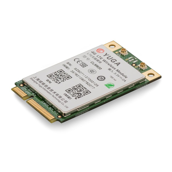
USB interface ±4 ±8 USIM interface ±4 ±8 Analog voice interface ±4 ±8 VBAT Power supply ±4 ±8 6 Structural and mechanical properties 6.1 Appearance CLM920_TE5 module is a double-sided PCBA . The appearance of the module is as below :... -
Page 39: Mini Pci Express Connector
CLM920_TE5 LTE Module Hardware Manual Figure 6- 1 CLM920_TE5 appearance 6.2 Mini PCI Express connector CLM920_TE5 module interface meets the PCI Express Mini Card 1.2 interface standard, PCI Express Mini Card connectors conforming to this standard can be used, such as Molex 679100002.
Need help?
Do you have a question about the CLM920_TE5 and is the answer not in the manual?
Questions and answers