Table of Contents
Advertisement
Quick Links
Advertisement
Table of Contents

Related Manuals for Terasic CY8CKIT-035


Summary of Contents for Terasic CY8CKIT-035
-
Page 2: Table Of Contents
CONTENTS INTRODUCTION TO THE PME EBK CHAPTER 1 ................3 1.1 Features ..............................3 1.2 About the KIT.............................4 1.3 PSoC Creator ..............................6 1.4 Getting Help ...............................6 PME EBK ARCHITECTURE CHAPTER 2 ....................7 2.1 Layout and Components..........................7 2.2 PSoC 4+1 Power Supervisor Solution on the PME..................8 PME EBK HARDWARE OVERVIEW CHAPTER 3 ................10... - Page 3 5.6 Voltage Regulator V4=1.8V ........................39 5.7 I2C/SMBus/PMBus Interface Connector ....................40 5.8 Layout...............................40 5.8.1 Top Layer ............................40 5.8.2 Ground Layer ............................41 5.8.3 Power Layer ............................41 5.8.4 Bottom Layer.............................42 5.8.5 Top Silkscreen ...........................43 5.9 Bill of Materials............................44 APPENDIX CHAPTER 6 ........................48 6.1 Revision History............................48 6.2 Copyright Statement ..........................48...
-
Page 4: Introduction To The Pme Ebk
Chapter 1 Introduction to the PME EBK In general terms, power management or power supervision is a combination of sequencing, monitoring and control of multiple regulators and/or point-of-load DC power converters in a system. Typical solutions for power management include multiple devices such as CPLDs, mixed-signal ASICs and/or limited-functionality and inflexible discrete devices. -
Page 5: About The Kit
shows a simplified block diagram of the most fundamental components on the PME Figure 1-1 EBK and how they interact to aid in understanding of the hardware. Not all hardware components are shown. Figure 1-1 PME EBK Block Diagram 1.2 About the KIT The PSoC Power Management Expansion board kit (PME) consists of: •... - Page 6 PME Example Firmware for the CY8CKIT-030 PSoC 3 Development Kit ○ Advanced Sequencer Power Supervisor Application Note (AN62496) “Voltage Sequencing with PSoC ® 3 and PSoC ® 5” ○ Application Note (AN60220) “Multiplexed Comparator using PSoC ® 3” ○ Datasheets for key PME EBK components ○...
-
Page 7: Psoc Creator
RTOS solutions, and production programmers to support PSoC 3. 1.4 Getting Help Certified as a Cypress Authorized Design Partner, Terasic offers design expertise in rapidly developing PSoC Solutions to get your products into production quickly and reducing your development and BOM costs. Terasic provides customized board designs for academia and industry. -
Page 8: Pme Ebk Architecture
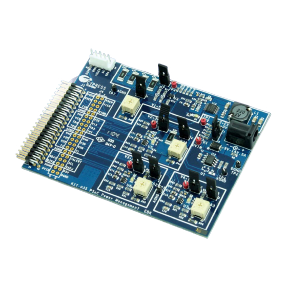
Chapter 2 PME EBK Architecture This chapter provides information about the architecture and block diagram of the PME EBK. 2.1 Layout and Components Photos of the PME EBK are shown in 2-2. They depict the layout of the Figure 2-1 Figure board and indicate the locations of the connectors and key components. -
Page 9: Psoc 4+1 Power Supervisor Solution On The Pme
Figure 2-2 PME PCB (Bottom) 2.2 PSoC 4+1 Power Supervisor Solution on the PME The PSoC Power Management EBK contains 4 DC voltage regulator circuits. They all have enable inputs to allow PSoC to control the power up and power down sequencing of the regulators as well as the necessary passive components to enable PSoC to measure their output voltage and load currents using its built-in ADC converter. - Page 10 pulse-width-modulated (PWM) outputs for regulator trimming and margining. The trim/margin PWM outputs from PSoC (labeled as TR[4]) are filtered with a single RC filter stage on PME EBK and fed into the voltage feedback input of the regulators. A single time-multiplexed window comparator is implemented in PSoC using 2 voltage DAC’s (to set the under and over voltage limits for each rail), 2 comparators and a programmable glitch filter.
-
Page 11: Pme Ebk Hardware Overview
Chapter 3 PME EBK Hardware Overview Figure 3-1 PME Hardware Components The Power Management EBK Board consists of a 12V primary input power source and 4 secondary voltage rails: V1=5V, V2=3.3V, V3=2.5V and V4=1.8V. Voltage rail V1 feeds power to the other three rails V2, V3 and V4. -
Page 12: 2X20 Pin Interface Header
PSoC Development Kit or CY8CKIT-030 PSoC 3 Development Kit. The header carries voltage enables, regulator voltage, regulator load currents and trim/margin control signals for each regulator on PME EBK. The I2C physical layer signals (SDA/SCL) from PSoC are also routed across this header to enable connection to an external host or management processor that supports standard I2C, SMBus or PMBus protocol interfaces. -
Page 13: Pme Ebk Headers And Jumpers
3.2 PME EBK Headers and Jumpers A number of headers and jumpers are provided on the PME EBK. The following table outlines the function of each item and the default configuration. Table 3-2 PME Jumper Settings Description Factory Default Designator Configuration 2×20 pin header for connecting to PSoC DVK 5-pin header for connecting an external host or management... -
Page 14: Example Projects For The Pme
Figure 4-1 CD Autorun Kit Menu NOTE: If auto-run does not execute, double-click AutoRun on the root directory of the CD. After the installation is complete, the kit contents are available at the following location: C:\Program Files\Terasic\PSoC Power Management EBK\1.0... -
Page 15: Hardware Setup
When installing the PSoC Power Management EBK software, the installer checks if your system has the required software. This includes PSoC Creator, PSoC Programmer, Windows Installer, .NET framework, Adobe Acrobat Reader, and KEIL Compiler. If these applications are not installed, then the installer prompts you to install all pre-requisite software, which is also available on the kit CD. - Page 16 2. Set the system to run at 5V using SW3 and set J6 “VDD DIG” and J7 “VDD ANLG” to VDD=5V using J6 and J7 as shown below: Figure 4-3 CY8CKIT-001 PSoC DVK Power Jumpers 3. Ensure that the LCD character display included with PSoC DVK is attached and that the LCD power jumper (J12) is in the ON position: Figure 4-4 CY8CKIT-001 PSoC DVK LCD Power Jumper CAUTION: Do not attach the PSoC Power Management EBK to the PSoC DVK until you have...
-
Page 17: Example Projects
CY8CKIT-030 PSoC 3 DVK 1. No jumper wires are required for the PSoC 3 DVK examples since the buttons and potentiometer are hardwired to GPIOs. Ensure that the LCD character display included with the PSoC 3 DVK is attached. 2. Set VDDD and VDDA to 5.0V using J10 and J11 Figure 4-5 CY8CKIT-030 PSoC 3 DVK Power Jumpers CAUTION: Do not attach the PSoC Power Management EBK to the PSoC 3 DVK until you have programmed the PSoC with one of the example projects. - Page 18 Figure 4-6 PSoC Creator Start Page showing Kits and Solutions The example projects will be displayed in the Workspace Explorer window as shown in the example below for the CY8CKIT-001 PSoC DVK: Figure 4-7 Workspace Explorer View Running the Example Firmware: CY8CKIT-001 PSoC DVK Make sure the hardware has been configured according to the Hardware Setup section.
- Page 19 CY8CKIT-009 PSoC 3 Processor Module In PSoC Creator, set the appropriate example project as active by right clicking on it in the Workspace Explorer and selecting Set As Active Project In PSoC Creator, select Debug > Program to program PSoC Remove power from the PSoC DVK and attach the PSoC Power Management EBK to Port A of the PSoC DVK On the PSoC Power Management EBK board, make sure the power jumper (J5) is set to...
- Page 20 6. On the PSoC Power Management EBK board, make sure the power jumper (J5) is set to “EXT”. Note that this is not the default setting for the J5 jumper. 7. Apply 12 VDC power to the PSoC Power Management EBK using J3 8.
- Page 21 Example 1: Advanced Sequencer Overview This example demonstrates the following features: 1. Voltage sequencing 2. Under-voltage/over-voltage monitoring using the window comparator for rapid fault detection If the project is running correctly, all 4 green LEDs on the PSoC Power Management EBK should be turned on and the debug LCD should display something like this: (See Figure 4-10)
- Page 22 Technical Details – Voltage Sequencing This example builds upon the Voltage Sequencer component discussed in Cypress Application Note ® ® AN62496 “Voltage Sequencing with PSoC 3 and PSoC 5”. The Voltage Sequencer component enables designers to control both the power-up and power-down sequence and timing of up to 16 secondary-side voltage supplies.
- Page 23 Figure 4-14 Voltage Sequencer Customizer General Tab For this example project, the key parameter settings are the number of rails (4), Auto Power Up and Auto Power Down settings and Rail Fail interrupts. Those settings enable the component to automatically sequence the regulators up and down with minimal firmware. Refer to AN62496 full details of the configuration options presented here.
- Page 24 1 is associated with regulator 1. Timing slot 2 with regulator 2 etc. Changing the checkbox assignments will change the sequence of powering up the regulators on PME EBK. Since rails 2 through 4 derive their input power from the output of regulator 1 (this is a hardwired connection on PME EBK), we will always need to power up rail 1 first.
- Page 25 Finally, click on the Monitor Tab to configure the rail monitoring options. Setting the MonType parameter to PGood will cause the sequencer to shut down when there is any failure on that rail. Setting it to None will cause the sequencer to ignore the PGood status on that rail. Changing the MonType to None for Rails 2, 3 and 4 will prevent the sequencer from shutting down the regulators when jumper J6 is removed from PME EBK, for example.
- Page 26 Figure 4-18 Time Multiplexed Over/Under Voltage Detection Hardware The time-multiplexing works according to this sequence: 1. The scaled regulator output for rail[n] (signal C[n]) is multiplexed into the window comparator 2. The under and over voltage limits for rail[n] are copied from SRAM to the DAC using DMA 3.
- Page 27 digital logic to constantly monitor the selected PGOOD inputs to make sure they are good. Any failure on any selected PGOOD input will cause an interrupt to the CPU core which will then call the Voltage Sequencer component power down API until the system is safely turned off. The firmware flowchart for the Example1 project is shown below (See Figure 4-19)
- Page 28 Example 2: 4+1 Power Supervisor Overview This example builds on the Example1 project and demonstrates a much more comprehensive power supervisor solution with the following features: 3. Power supply sequencing 4. Power supply voltage and current measurement accurate to better than 1% 5.
- Page 29 Figure 4-21 LCD Display - Currents The 0.1mA reading in the top left corner indicates the units of the 4+1 power supply current measurements. The next 2 numbers on the 1st line of the display indicate the measured 12 V primary input load current value and the measured 5 V rail load current value.
- Page 30 When the trimming menu is displayed, pressing and holding SW1 on the CY8CKIT-001 PSoC DVK (SW2 on the CY8CKIT-030 PSoC 3 DVK) for a longer period will enable manual trimming control for the next secondary regulator. To get back to the main voltage display menu, cycle through all 4 manual trim menus by pressing and holding SW1 on the CY8CKIT-001 PSoC DVK (SW2 on the CY8CKIT-030 PSoC 3 DVK) for a longer period.
- Page 31 Figure 4-23 ADC Converter Schematic For measuring voltages, the Delta-Sigma ADC is configured to use a ±2048 mV input range with a 2048 mV reference (generated by doubling the internal 1024 mV reference) on the negative input terminal, yielding an actual single-ended voltage measurement range of 0 to 4096 mV. This range is used to measure the voltages of each of the regulator rails on the PSoC Power Management EBK.
- Page 32 the resolution of the ADC and the time taken to switch inputs and change ADC configuration. At a CPU clock frequency of 24MHz (as used in Example2), the time taken to execute those fundamental tasks is outlined below: 1. Using the ±2048 mV range: 65 μs per reading 2.
- Page 33 voltage. Typical power supplies respond in this manner, however for others that do not, this circuit both internal to PSoC and external can be customized for the specific power supply chosen (for example: inverting the PWM output such that a decrease in PWM duty cycle decreases the regulator output voltage).
- Page 34 Margining is similar to trimming but is used for a different purpose. In that case, the rails are intentionally set to their upper or lower limits to enable system designers to verify that their systems work at both extremes of the voltage rail tolerances. For example, if a 5 V rail is used in the system and specified to have an accuracy of +/- 5%, margining will set the rail to 5 V -5% to enable system verification.
- Page 35 Reset or Power On Display LCD Intro Message Start PWM Trim Circuits Start ADC Conversions Start Window Comparator H/W Block Start Voltage Enable Sequencer Regulator n Component Execute Ramp Delay for Slot n PGOOD[n] Execute Up Delay for Slot [n] n <= 4? n=n+1 PGOOD...
-
Page 36: Power Management Component Library
Figure 4-26 Example2 ADC ISR Thread Firmware Flowchart 4.5 Power Management Component Library The example projects provided use custom PSoC Creator components that are not included with the standard PSoC Creator Software install. These are the Voltage Sequencer, Comparator Controller and Comparator Glitch Filter Components. -
Page 37: Using Components In Your Own Projects
4.6 Using Components in Your Own Projects NOTE: This section does not apply to PSoC Creator 2.0 or later as the required components are included in the tool component library. The Power Supervisor PSoC Creator components are provided in Library form so that you can easily add them to your own projects. -
Page 38: Schematics
Chapter 5 Schematics 5.1 Primary 12V Power Input... -
Page 39: Dvk Connector And Debug Test Points
5.2 DVK Connector and Debug Test Points 5.3 Voltage Regulator V1=5V... -
Page 40: Voltage Regulator V2=3.3V
5.4 Voltage Regulator V2=3.3V 5.5 Voltage Regulator V3=2.5V 5.6 Voltage Regulator V4=1.8V... -
Page 41: I2C/Smbus/Pmbus Interface Connector
5.7 I2C/SMBus/PMBus Interface Connector 5.8 Layout 5.8.1 Top Layer... -
Page 42: Ground Layer
5.8.2 Ground Layer 5.8.3 Power Layer... -
Page 43: Bottom Layer
5.8.4 Bottom Layer... -
Page 44: Top Silkscreen
5.8.5 Top Silkscreen... -
Page 45: Bill Of Materials
5.9 Bill of Materials Item Description Designator Quantity Value Manufacturer Manufacturer Part# CAP .1UF 25V C1,C4,C9 0.1μF, Kemet C0805C104K3RAC CERAMIC X7R 7210 0805 CAP CER 22UF C2,C5,C6 22μF, Murata Electronics GRM31CR61E226 25V X5R 1206 North America KE15L CAP CER 3300PF 3.3nF, Murata Electronics... - Page 46 2.2A SMD RES 0.0 OHM R2,R8 Panasonic-ECG ERJ-6GEY0R00V 1/10W 5% 0805 RES 51.0K OHM R3,R11,R13 51kΩ Susumu RG2012P-513-B-T 1/8W 0.1% 0805 RES 20.0K OHM 22kΩ Susumu RG2012P-203-B-T 1/8W 0.1% 0805 RES 2.21 OHM R5,R6,R7,R9, 2.21Ω Stackpole Electronics RNCF0603BKC2R 1/16W 0.1% 0603 R10,R15,R17, R18,R19,R23, R32,R33,...
- Page 47 RES 20K OHM 20kΩ Panasonic - ECG ERJ-6GEYJ203V 1/8W 5% 0805 RES 33 OHM 2W 33Ω Stackpole Electronics RHC2512FT33R0 1% 2512 SMD RES 634K OHM 634kΩ Panasonic - ECG ERJ-6ENF6343V 1/8W 1% 0805 RES 1M OHM R40,R50,R61 1MΩ Panasonic - ECG ERJ-6GEYJ105V 1/10W 5% 0805 RES 365K OHM...
- Page 48 TEST POINT 43 TP2,TP5,TP6, Keystone Electronics 5001 HOLE 65 PLATED BLACK IC AMP Maxim Integrated MAX4080TASA+ CURRENT Products SENSE 8-SOIC HIGH-SIDE Zetex ZXCT1009FTA CURRENT MONITOR IC CONV Texas Instruments TPS54226PWPR STP-DWN SYNC 2A 14HTSSOP IC REG LDO ADJ U5,U6,U7 Analog Devices Inc ADP3331ARTZ-RE 200MA SOT-23-6 BUMPER...
-
Page 49: Chapter 6 Appendix
Chapter 6 Appendix 6.1 Revision History Version Change Log V1.0 Initial Version (Final) 6.2 Copyright Statement Copyright © 2011 Terasic Technologies. All rights reserved. - Page 50 Mouser Electronics Authorized Distributor Click to View Pricing, Inventory, Delivery & Lifecycle Information: Terasic P0090...
Need help?
Do you have a question about the CY8CKIT-035 and is the answer not in the manual?
Questions and answers