Advertisement
Table of Contents
- 1 Table of Contents
- 2 Location of PC Boards
- 3 Electronic Specification
- 4 Measurement Setup
- 5 Service Aids
- 6 Instruction on CD Playability
- 7 Software Version Check & Upgrade
- 8 Disassembly Diagram
- 9 Block Diagram
- 10 Wiring Diagram
- 11 Layout Diagram
- 12 Exploded View
- 13 Revision List
- Download this manual
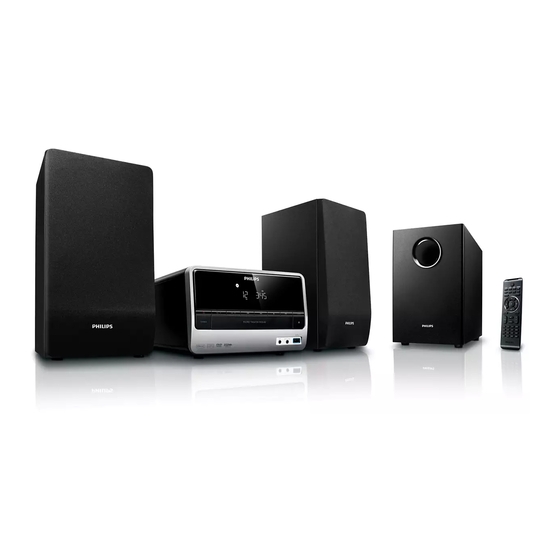
DVD Micro System
TABLE OF CONTENTS
Location of PC Boards ............................................. 1-1
Electronic Specification ............................................. 1-2
Measurement Setup ................................................ 1-3
Service Aids............................................................... 1-4
Instruction On CD Playability ........................... 1-5 to 1-6
Software Version Check & Upgrade ........................ 2-1
Malfuction Check Chart ............................................. 2-2
Disassembly Diagram................................................ 3-1
Block Diagram ......................................................... 4-1
Wiring Diagram ......................................................... 4-2
Small Board .................................................................. 5
Circuit diagram ...................................................... 5-1
Layout diagram ...................................................... 5-1
LCD Display Board ...................................................... 6
Circuit diagram ...................................................... 6-1
Layout diagram ...................................................... 6-2
Power Board ............................................................... 7
Circuit diagram ............................................. 7-1 to 7-2
Layout diagram ...................................................... 7-3
2011
SW 1131
Version 1.1
ReWritable
Decoder Board ............................................................ 8
Circuit diagram ............................................. 8-1 to 8-7
Layout diagram ...................................................... 8-8
Exploded View ......................................................... 9-1
Service Partlist .......................................... 10-1 to 10-2
Factory Partlist ...................................................... 11-1
Revision list............................................................. 12-1
MCD183
Recordable
3141 785 34011
Advertisement
Table of Contents

Related Manuals for Philips MCD183/05


Summary of Contents for Philips MCD183/05
-
Page 1: Table Of Contents
MCD183 DVD Micro System Recordable ReWritable TABLE OF CONTENTS Location of PC Boards ..........1-1 Decoder Board ............8 Electronic Specification ..........1-2 Circuit diagram ..........8-1 to 8-7 Measurement Setup ..........1-3 Layout diagram ............8-8 Service Aids............... 1-4 Exploded View ............ -
Page 2: Location Of Pc Boards
Location of PC Boards Power Board VFD Display Board USB/Headphone Board Decoder Board VERSION VARIATION Type /Versions: MCD183 Service policy Board in used: USB/HEADPHONE BOARD LCD DISPLAY BOARD POWER BOARD DECODER BOARD Type /Versions: MCD183 Features Feature diffrence VOLTAGE SELECTOR ECO STANDBY - DARK * TIPS : C -- Component Level Repai r. -
Page 3: Electronic Specification
Electronic Specification AMPLIFIER SPEAKERS Rated Output Power ....50W+2X25W RMS Speaker Impedance ......... 2x4ohm+8ohm Signal-to-noise ratio ........≥65dBA Speaker Driver, base .............5” Frequency response ....100Hz--15kHz ±3dB Speaker Driver, tweeter ..........3” Aux Input ........ 0.5V/ RMS 47kohm Frequency Response ....100Hz +5dB+/-5 15KHz DISC GENERAL INFORMATION Laser Type ........ -
Page 4: Measurement Setup
MEASUREMENT SETUP Tuner FM Bandpass LF Voltmeter 250Hz-15kHz e.g. PM2534 e.g. 7122 707 48001 RF Generator e.g. PM5326 S/N and distortion meter e.g. Sound Technology ST1700B Use a bandpass filter to eliminate hum (50Hz, 100Hz) and disturbance from the pilottone (19kHz, 38kHz). Tuner AM (MW,LW) Bandpass LF Voltmeter... -
Page 5: Service Aids
SERVICE AIDS WARNING All ICs and many other semi-conductors are susceptible to electrostatic discharges (ESD). Careless handling during repair can reduce life drastically. When repairing, make sure that you are connected with the same potential as the mass of the set via a wrist wrap with resistance. Keep components and tools also at this potential. -
Page 6: Instruction On Cd Playability
INSTRUCTIONS ON CD PLAYABILITY Customer complaint "CD related problem" Set remains closed! check playability playability ok ? For flap loaders (= access to CD drive possible) "fast" lens cleaning cleaning method is recommended check playability playability ok ? Play a CD for at least 10 minutes check playability playability... - Page 7 INSTRUCTIONS ON CD PLAYABILITY PLAYABILITY CHECK LIQUID LENS CLEANING Before touching the lens it is advised to clean the surface of the lens by blowing clean air over it. For sets which are compatible with CD-RW discs This to avoid that little particles make scratches on use CD-RW Printed Audio Disc ....7104 099 96611 the lens.
-
Page 8: Software Version Check & Upgrade
Software Version Check & Upgrade Upgrade software 1.Download the software from Philips support website: http://www.philips.com/support 2. Load the CD Disc or USB device with software,Software upgrade procedure starts automatically Upgrading Waiting a minute Read USB Software upgrade finish. Software version and date check 1, Power on the unit whithout loading the USB and Disc in it, then press the “811502”... - Page 9 Malfunction Follow Check Chart No display No power No sound Time/Clock does not work Check if the Power Cord Adjust the volume Plug in the power cord Check the files or folders in is connected USB or others devices has not exceeded the certain limit Check if the speakers Switch on the Timer...
-
Page 10: Disassembly Diagram
Disassembly Diagram A,Open the DVD tray and then loose 2pcs C,Loosed 4pcs screws(3 x 10 BA)to remove B,Remove the top cabinet. B1.Loose 2pcs screws(3 x 12 KB) of the L&R sides(front-end) screws to remove the door the Power Board B2.Loose 2pcs screws(3 x 8 KB) of the L&R sides(back-end) B3.Loose 1pcs screws(3 x 10 FA) of the back sides F,Remove Front Cabinet E,Loose 4pcs screws(3 x 10 PWA) -
Page 11: Block Diagram
Block Diagram MCD183 M3.3V 1.8V MAIN BOARD SONY pick up 313AAD Y U V DVD Loader Loader motor driver CD5954 Main chipset S-VIDEO Open/Close Driver OPEN DOOR Door Detect COAXIAL CLOSE DOOR M3.3V SERIAL EEPROM OPTICAL 24C02 M3.3V SDRAM 4M * 16 M12L64164A-7T M3.3V FLASH... -
Page 12: Wiring Diagram
Wiring Diagram DVD Loader Decoder Board AC IN Power Board Scart Board VFD Display Board Headphone Board... - Page 13 Small Board -- Layout & Circuit Diagram 35-MCD183-02A1 35-MCD183-03A1 From dvd decoder ASP 12V J203 CN203 16:9 ASP=7.5V-8V J1501 4:3 ASP=12V CVB1 RGB V/S=3V 4P/2.0 VIDEO V/S=0V 20.VIDEO IN 19.VIDEO OUT CN201 18.FS GND MU-H 17.VIDEO GND RO-H 16.FS LO-H 15.RED GND-H 14.REMOTE GND...
- Page 14 LCD Display Board -- Circuit Diagram DISPLAY BOARD LCD101 35-MCD183-01A1 R1001 R1003 R1017 4.7K 100R R1004 LED1000 100R R1002 Q1000 REMOTE 8050 4.7K S1000 Q1002 R1007 R1009 8550 IC1001 R1006 R1016 C1005 4.7K 47 1/8W seg7 cup2 SEG7 seg8 C1003 cup1 SEG8 seg9...
-
Page 15: Layout Diagram
LCD Display Board -- Layout Diagram... - Page 16 Power Board -- Circuit Diagram -- Part1 H_VCC MOS3 EI33 STTH2003 CT CON_VCC 68UF/400V 103/1KV 471/400V 103/630V 68K/1W 7UH/4A &' GBU4J 1000 U/35V 68UF/400V FR157 471/400V 1000 U/35V R88-R91 100R 102/1KV MOS2 FR104 8N60 221/1KV 2.2K 0.22U/275V 100R TL431 EL817 47UF/50V T68-26A 100K...
- Page 17 Power Board -- Circuit Diagram -- Part2 CE21 470UF/25v Vfan CE26 CE24 5.1R 470U/25V 470U/25V 4.7K 2P/2.5 BAND 470uf/16v CE18 CE19 CE27 470uf/16v 470U/25V 103/50V 8050 CE25 CE14 470U/25V CE11 1uf/25V 4.7uf/50v CE28 103/50V 9014 100U/25V 2.2K 8550 470R IN1+ 0.15R 1W OUT1+ IN2+...
- Page 18 Power Board -- Layout Diagram...
- Page 19 Decoder Board -- Circuit Diagram MCU+5V 400mA 400mA AZ1117H-3.3 OUT1 OUT2 450mA CB10 + CE9 CB11 0.1uF 100uF/16V 0.1uF 220uF/16V 0.1uF SOT223 L113 0R/1206 VCC_5V 1100mA FM5V SM9435A 0R/1206 CE111 0.1uF 100uF/16V CE118 C692 0.1uF 470uF/10V/8X7 220uF/16V 2.2uF 350mA AZ1117H-ADJ OUT1 OUT2 ECO-POWER...
- Page 20 Decoder Board -- Circuit Diagram 89L_3V3 89L_3V3 47uH/DIP DV33 SP-A ADACVDD 150uH/DIP APLLVDD3 RFV18-1 CB12 0.1uF 89L_3V3 RFVDD3 DQ[0..15] DQ[0..15] R1052 LIMIT DACVDD3 DACVDD3 L105 TP10 RFV18-2 CB145 0.1uF CB153 R1053 100K MA[0..11] MA[0..11] TP11 CB149 CB150 CB151 TP12 4.7uF 0.1uF DQM[0..1] DQM[0..1]...
- Page 21 Decoder Board -- Circuit Diagram SDRAM (Dual Layout) DQ[0..15] DQ[0..15] MA[0..11] MA[0..11] DQM[0..1] DQM[0..1] SD33 BA[0..1] BA[0..1] R1094 10K SDCKE DCLK DCLK R1095 10K DCS# RAS# RAS# MA10 DQ10 CAS# CAS# A10/AP DQ10 MA11 DQ11 DQ11 DBA0 DQ12 BA0/A13 DQ12 DBA1 DQ13 BA1/A12...
- Page 22 Decoder Board -- Circuit Diagram DVD-LIN CE30 10uF/10V R1098 R1100 LINE_L_OUT R102 CB55 3.3K 0.1uF DVD/MUTE RCA3X2 CE37 10uF/10V AV6-8.4-13B V_G/Y 2N3904 0PEN/47K 0PEN/100pF 2N3904 TP39 TP40 R103 1.8uH/SMD 160 1% 100K R104 TP41 LINE_L_OUT TP42 2.2K 47pF 47pF R106 TP43 LINE_R_OUT TP44...
- Page 23 Decoder Board -- Circuit Diagram 1N4148 1N4148 DVD/MUTE MUTE R756 4.7K MUTE1 1N4148 R757 MUTE_MCU CE98 4.7uF/16V AUX-IN AUX-RIN VCC_27V AUX-LIN L120 FB/5A FB/5A FM5V CE125 CE124 CD263/680UF/35V MUTE1 HP_MUTE CD263/220UF/35V ESD0402/SMD R340 TPA3123D2 NS/EZJZ1V800AA NS/EZJZ1V800AA TP58 ESD0402/SMD 1N4148 R1033 22K DS-STB USB-DET CB85...
- Page 24 Decoder Board -- Circuit Diagram FM5V FM-RIN R375 R376 FM-RIN FM-LIN 120R FM-LIN SI4702 CE77 SI4704 120nH/nc R375 0/NC 3.3V/SMD TUNER_RST SI470X CD11X/100UF16V/D6.3H7 TUNER_RST R376 SCLK SCLK SSDA 0/NC SSDA DOUT RFIN C127 100P C128 0.47uF FM-LIN LOUT C129 0.47uF FM-RIN RFGND ROUT...
- Page 25 Decoder Board -- Layout Diagram...
-
Page 26: Exploded View
Exploded View... -
Page 27: Revision List
12-1 REVISION LIST Version 1.0 ( 3141 785 34010 * Initial Release; Version 1.1 ( 3141 785 34011 * Add partlist for /77;...