
Subscribe to Our Youtube Channel
Related Manuals for Lanner LVC-5000-B0


Summary of Contents for Lanner LVC-5000-B0
- Page 1 In-Vehicle Computing Hardware Platforms for mobile applications LVC-5000-B Series V1.0 User's Manual Release date: 2014/12/30...
- Page 2 Resource Website installed and used in accordance with the instruction manual, may cause harmful interference to radio Lanner http://www.lannerinc.com communications. Operation of this equipment in a residential area is likely to cause harmful interference Product Resources http://assist.lannerinc.com in which case the user will be required to correct the interference at his own expense.
- Page 3 Mechanical compliance Revision History Vibration: Version Date Description 2014/12/30 Official release General Vibration (operating): Refer to MIL-STD-810G, • Method 514.6, Procedure I (Transportation), Category 4 – Common carrier (US highway truck vibration exposure) General Vibration (non-operating): Refer to MIL-STD- • 810G, Method 514.6, Procedure I (Transportation), Category 24 –...
-
Page 4: Table Of Contents
Table of Contents Chapter 1: Introduction Model Summaries System Specifications Package Contents Chapter 2: System Components System Drawing Block Diagram: The MainBoard Front Components Rear Components Chapter 3: Motherboard Information Inside LVC-5000-B Series Jumpers & Connectors on the Motherboard Jumpers & Connectors on the Motherboard Jumpers &... -
Page 5: Chapter 1: Introduction
Chapter 1: Introduction Model Summaries LVC-5000-B0 (4 POEs): Thank you for choosing Lanner LVC-5000-B series. The 1.7 GHz Intel® Core™ i7-3517UE In-Vehicle Mobile LVC-5000-B series is a rugged vehicle PC designed NVR, DDR3 4GB SO-DIMM x1, 2.5” external Drive to be integrated on-board for fleet management Bay x1(support to TB grade HDD), Mini-PCIe x2 with applications and vehicle monitoring. -
Page 6: System Specifications
System Specifications Package Contents 273.8x188.0x72.0 Your package contains the following items: Dimensions (unit: mm) 308.0x188.0x100.6 (w/ suspension kit) LVC-5000-B series Fanless Embedded System with Processor Intel 847E/i7-3517UE vibration kit Chipset Intel HM65 Technology DDR3 SO-DIMM x1 (default 4GB) System Terminal Block Connectors: •... -
Page 7: Chapter 2: System Components
Chapter 2: System Components System Drawing Mechanical dimensions of the LVC-5000-B series Unit: mm... - Page 8 Notes: This mechanical drawing set is for reference only. Dimensions for all models B0, B1, B2 and B3 are the same but I/O connectors may vary due to planning purposes.
-
Page 9: Block Diagram: The Mainboard
Block Diagram: The MainBoard LVC-5000-B series comes with various CPU and I/O options. Thus, there are more than one block diagrams to be presented in the following. LVC-5000-B0 block diagram:... - Page 10 LVC-5000-B1/B2 block diagram:...
- Page 11 LVC-5000-B3 block diagram:...
-
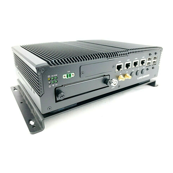
Page 12: Front Components
Front Components All LVC-5000-B series models share common I/O components at the front panel. Component Description F1 LED Indicators x 6 for HDD status 3G status PoE stats component status Power WiFi status Ignition status F2 Remote Power Switch 1x2-pin terminal block for distant power-on/off control F3 Four 10/100/1000Mbps LAN Four RJ-45 (provided by Intel 82583V) jacks with LED indicators ports... -
Page 13: Rear Components
Rear Components All LVC-5000-B series models show variations in terms of rear panel I/O components. LVC-5000-B0 Component Description R1 Multiple-I/O Connector A 26-pin male connector configured as followed: • 4x DI ( 5V or 12V TTL selectable) • 4x DO (12V TTL , Max. 100mA) •... - Page 14 LVC-5000-B1/B2/B3 Component Description R1 Multiple-I/O Connector A 26-pin male connector configured as followed: • 4x DI ( 5V or 12V TTL selectable) • 4x DO (12V TTL , Max. 100mA) • 2x DO control Relay support 9~36V@max 2A each • 2x DI to Ignition MCU as remote control ( 5V TTL) •...
-
Page 15: Chapter 3: Motherboard Information
Inside LVC-5000-B Series Though all models of LVC-5000-B series share the same main motherboard, they come in card/board combinations due to slight differences in specifications. Please see the following for references. LVC-5000-B0 At A Glance The main motherboard PoE Power Board: LVK-POE60W01... - Page 16 LVC-5000-B1/B2 At A Glance The main motherboard PoE Power Board: LVK-POE60W01 Add-on card: LVK-CBPE1...
- Page 17 LVC-5000-B3 At A Glance The main motherboard PoE Power Board: LVK-POE60W01 Add-on card: LVK-CBSA1...
-
Page 18: Jumpers & Connectors On The Motherboard
Jumpers & Connectors on the Motherboard POEIO1 LAN1/LAN2/LAN3/LAN4 USBB1 USBB2 PRJK1 HDMI1 VGAA1 MIO2 DVID1... - Page 19 SPI1 AUDIOIN1 LPC1 PKMB1 PS4M1 COMSLT1 MPCIE2 MPCIE1 PS4S1 PCOM1 SCT2 CMOS1 PCOM2 SCT1 COMB1 SATAB1 COMB2 MIO3...
-
Page 20: Jumpers & Connectors On The Motherboard
Jumpers & Connectors on the Motherboard (Bottom side) SIM2 SIM1 DIMM... -
Page 21: Jumpers & Connectors On The Poe Power Board
Jumpers & Connectors on the PoE Power Board Top Side ATX1 POEIO1 Bottom Side... -
Page 22: Jumpers & Connectors On The Add-On Card Lvk-Cbpe1
Jumpers & Connectors on the Add-on Card LVK-CBPE1 MPCIE1 CN1 (module optional) LAN1 CAN1 MIO1 (to connect with MIO3 on the main motherboard) -
Page 23: Jumpers & Connectors On The Add-On Card Lvk-Cbsa1
Jumpers & Connectors on the Add-on Card LVK-CBSA1 MPCIE1 LAN1 CAN1 MIO (to connect with MIO3 on the main motherboard) -
Page 24: Connectors And Jumpers List
Connectors and Jumpers List Table 3.1 Connector List for LVK-POE60W01 Board Labels Function ATX1 ATX Power Connector POEIO1 Connector for connecting to the mainboard PoE setting Table 3.2 Connector List for LEB-5000 Board Labels Function AUDIOIN1 Line-in/Mic-in Connector CMOS1 Cleaning CMOS Data Including RTC CF Card Slot RS-232 Connector for MCU Programming Distant Power on/off Control Connector... -
Page 25: Jumper Settings & Connector Pinouts
Jumper Settings & Connector Pinouts LVB-5000 Board COM3 RS-232 Serial Port (COMB1): RS-232 DB9 COM port connected to and enabled by an internal COM LVK-POE60W01 connector ATX1: ATX Power connector which connects to PS4M1 on the mainboard. Pin No. Description SP3_DCD Pin No. - Page 26 SCT1, SCT2: Select COMB2 Protocol Setting PS4M1: Connect to the ATX1 power connector on the LVK-POE60W01 board Pin No. Pin Name DCIN_VCC DCIN_VCC AUDIOIN1: Line-in and Mic-in Connector 2 4 6 1 3 5 Pin No. Pin No. Pin Name MIC_in_R MIC_in_L Audio_in_R...
- Page 27 SATAB1 (SATA0): SATA7-pin signal connector for a MIO3: 2x50 Dual-Row Socket for any extension board 2.5” disk drive on the mainboard: Pin No. Description Pin Name Pin Name HDA_BCLK_PCH PCH_SATATXP0 PCH_SATATXN3 HDA_SYNC_PCH PCH_SATATXN0 PCH_SATATXP3 HDA_RST_N_PCH HDA_SDIN1_PCH PCH_SATARXN0 PCH_SATARXP0 PCH_SATARXN3 HDA_SDO_PCH PCH_SATARXP3 SPK_PCH VCC3P3_SB...
- Page 28 POEIO1: Connector for Connecting to the POE DVI-D Connector (DVID1): A single link DVI-D Connector power board LVK-POE60W01 Pin No. Description Pin No. Description PCH_DDPC_0N PCH_DDPC_0P DVI_SCL DVI_SDA Pin No. Description Pin No. Description PCH_DDPC_1N PCH_DDPC_1P VPORT_OUT3 VPORT_OUT2 VPORT_OUT3 VPORT_OUT2 VCC5_PS VPORT_OUT3 VPORT_OUT2...
- Page 29 Multiple I/O Connectors (MIO2): 26-pin MPCIE1: Mini-PCIe Connector with one SIM Card external Multiple I/O for functions in Audio, serial Reader(SIM1). It supports both Wi-Fi and 3G module. communication, Digital In/Out, Ignition detection input for automatic wake-up function Signal Signal PCIE_WAKE_N VCC3P3_PS Signal...
- Page 30 SIM Card Socket (SIM1/SIM2): SIM card slots Dual USB 2.0 Ports USB0 & USB1(USBB1) 5 6 7 8 1 2 3 4 Pin No. Pin Name VCC5 USBD0N USBD0P Pin No. Description VCC5 UIM_PWR USBD1N UIM_RST USBD1P UIM_CLK UIM_VPP UIM_DAT Dual USB 2.0 Port s USB2 &...
- Page 31 PS/2 Keyboard and Mouse Connector (PKMB1) SW1 & SW2: Function Select Default Pin1 & Pin2 ON, Pin3 & Pin4 OFF 1 2 3 4 Pin No. Signal Pin No. Signal VCC5_KB KCLK Pin No. Setting Description MDAT On/Off Detect Power Good KDAT On/Off Low Power Detect...
- Page 32 LVK-CBPE1 Board MIO3: 2x50 Dual-Row Socket for any extension board MPCIE1: Mini-PCIe Connector with one SIM Card Reader(SIM1). It supports both Wi-Fi and 3G module. Pin Name Pin Name PCH_SATATXN3 PCH_SATATXP3 PCH_SATARXN3 PCH_SATARXP3 VCC3P3_SB Signal Signal VCC3P3_PS VCC3P3_SB WAKE_N VCC3.3 VCC3P3_PS VCC3P3_SB VCC3P3_PS...
- Page 33 LAN1: Ethernet LAN port on the board CAN1: Vehicle’s Electronic Control Unit Junction (D-sub) Pin No. Description J1850-/J1708- Pin No. Description MDI0P CAN_H/J1939+ MDI0N K_LINE MDI1P CAN_L/J1939- MDI1N J1850-/J1708- TCL1 J1850+/J1708+ TCL2 J1850+/J1708+ MDI2P Battery 12V/24V In MDI2N MDI3P MDI3N 100_LED 1000_LED ACTLED+...
- Page 34 LVK-CBSA1 Board MIO3: 2x50 Dual-Row Socket for any extension board MPCIE1: mSATA slot Pin Name Pin Name PCH_SATATXN3 PCH_SATATXP3 PCH_SATARXN3 PCH_SATARXP3 Signal Signal VCC3P3_SB VCC3P3_PS VCC3P3_PS VCC3P3_SB VCC3P3_PS VCC3P3_SB VCC1P5 VCC3P3_PS VCC3P3_SB VCC3P3_SB PCH_PCIE_RXN8 PCH_PCIE_RXP8 PCH_PCIE_TXN8 PCH_PCIE_TXP8 PCIE_CKN8 PCIE_CKP8 PCH_SATARXP3 VCC3P3_PS PLTRST_BUF1_N SMBCLK_RESUME...
- Page 35 LAN1: Ethernet LAN port on the board CAN1: Vehicle’s Electronic Control Unit Junction (D-sub) Pin No. Description J1850-/J1708- Pin No. Description MDI0P CAN_H/J1939+ MDI0N K_LINE MDI1P CAN_L/J1939- MDI2P J1850-/J1708- MDI2N J1850+/J1708+ MDI1N J1850+/J1708+ MDI3P Battery 12V/24V In MDI3N ACTLED+ ACTLED- 1000_LED 100_LED CN1: Interpreter Module Connector...
-
Page 36: Chapter 4: Hardware Setup
Chapter 4: Hardware Setup Installing a HDD/SSD Disk Drive Preparing the Hardware Installation The system provides an externally accessible 2.5” SATA disk drive tray. Please see the instructions below for installation. WARNING: To reduce the risk of personal injury, Locate the 2.5” SATA disk drive tray on the front electric shock, or damage to the equipment, panel. -
Page 37: Mini-Pcie Wireless Network Module Installation
Mini-PCIe Wireless Network Module 3. Gently lift the bottom compartment to access the internal components. Installation 1. Turn the system upside down. 2. Loosen and remove the circled screws on four sides as circled below. 4. Locate the mini-PCIe sockets on the mainboard 5. -
Page 38: Connecting Power
Connecting Power Connect the LVC-5000 to a +12V or +24V vehicle battery. The DC power-in connector comes with a 3-pin terminal block for its Phoe- nix contact. This power socket can only accept the power supply with the right pin contact so be cautious when inserting power to the system. -
Page 39: Chapter 5: The Flow Chart
Chapter 5: The Flow Chart The flow chart section contains all flow chart used in the system. The flow chart describes the system’s behavior on powering on and off the system via power ignition control or on/off switch when the appropriate timer control parameters are set. -
Page 40: Appendix A: Using The Ignition System Manager (Ism)
Appendix A: Click Cancel to exit the ISM program. Using the Ignition System Manager (ISM) The Ignition System Manager (ISM) is a software that can monitor the system’s voltage level and configure the COM5 features that the Power Ignition Module provides. For sample ISM code, see ISM folder under LVC-5000 Utility on the Driver and Manual CD. -
Page 41: Appendix B: Digital Input/Output
For sample DIO code, see SuperIO folder under LVC-5000 Utility on the Driver and Manual CD. Make sure that you have installed the Lanner GPIO driver as instructed below. Driver Installation Before you could access or control the operation of the G-sensor, GPS and Digital I/O functions, install the Answer “Yes”... - Page 42 Choose to select the hardware Manually Click HaveDisk to locate the L_IO.inf file Choose Show all device and click Next. Select the L_IO.inf Select OK to confirm with the installation Click HaveDisk to locate the L_IO.inf file...
- Page 43 Select the Lanner IO driver and click Next. To verify the GPIO driver installation, do the following steps: Right-click on the My Computer icon, and then select Properties form the menu. Click the Hardware tab, then click the Device Manager button.
- Page 44 A sample DIO program in C: ioaccess.c: IO access code for Lanner Platfomr Digital IO program #include <time.h> ********************************************************* #include <stdint.h> **********************/ #include <fcntl.h> #include <errno.h> #include <string.h> #define delay(x) usleep(x) #include “../include/config.h” #endif #ifdef DJGPP #ifdef MODULE /* standard include file */ #include <linux/kernel.h>...
- Page 45 #include <machine/bus.h> outportb(INDEX_PORT, 0xAA); #include <machine/resource.h> return; #endif #endif unsigned char read_SIO_reg(int LDN, int reg) /* local include file */ outportb(INDEX_PORT, 0x07); //LDN register #include “../include/ioaccess.h” delay(5); outportb(DATA_PORT, LDN); #if (defined(MODULE) || defined(DIRECT_IO_ACCESS) || delay(5); defined(KLD_MODULE)) outportb(INDEX_PORT, reg); delay(5); return(inportb(DATA_PORT)); *------------------------------------------------------------------------- ----- * LEB-5000 Version V1.0...
- Page 46 exit_SIO_config(); return; void dio_set_output(unsigned char out_value) enter_SIO_config(); write_SIO_reg(0x6, 0xf1, ((read_SIO_reg(0x6, 0xf1)& 0xF0)|out_value)); exit_SIO_config(); return; unsigned int dio_get_input(void) unsigned int tmp=0x00; enter_SIO_config(); tmp=read_SIO_reg(0x6, 0xA2)& 0x0f; exit_SIO_config(); return tmp; //====================================== ======================================== ================= #endif...
-
Page 47: Appendix C: Accessing The Digital Accelerometer Data
Driver Installation To access the G-Sensor data, use the following instructions: Make sure you already installed the Lanner GPIO int main(int argc, char* argv[]) driver on your LVC-5000 as instructed in Appendix B. To access the Gsensor data, locate the adxl345_v001 folder and execute the executable file adxl345 and it adxl345_init () ;... -
Page 48: Appendix D: Accessing The Gps Data
Appendix D: To access the GPS data, follow the following steps: Accessing the GPS Data Select Programs from the Start menu on your windows from the LVC-5000 and open the Hyper Terminal program. The LVC-5000 employs GPS module from GPS ublox NEO- 6Q for vehicle tracking and navigation system. - Page 49 Specify the following communication parameters: Bits per Second: 9600 Data Bits: 8 Parity: None Stop Bit: 1 Flow Control: None 9600 The hyper terminal should display GPS data:...
-
Page 50: Appendix E: Programming System Watchdog Timer
Appendix E: #include “F81865.h” Programming System Watchdog Timer of the #define PARAMETER_HELP “\n”\ “The F81865 GPIO utility of Lanner\n”\ LVC-5000-B “-------------------------------------\n”\ “Usage:\n”\ A watchdog timer is a piece of hardware that can be used to automatically detect system anomalies and reset “... - Page 51 “ Watchdog c (nPort, nValue) ; Watchdog timer.\n”\ “ CaseOpen Check case opened state.\n”\ “ printf (b “ #%d = %d\n”, nPort, nValue) ; CaseOpen_Clear Clear case open state.\n”\ “ port_number The port number.\n”\ “ value 1 for on and 0 for off.\n”\ return 0 ;...
- Page 52 // Clear case open state return 0 ; int mCaseOpen_Clear (int argc, char* argv[]) CHECK_ARGC (2) ; // Watchdog CaseOpen_Clear () ; int mWatchDog (int argc, char *argv[]) BOOL bOpen = CaseOpen () ; if (argc != 3 && argc != 2) RETMSG (-1, PARAMETER_HELP) ;...
- Page 53 {“DIO_IN” , mDIO_IN // No match argument {“DIO_OUT” , mDIO_OUT RETMSG (-1, “Wrong Argument\n”) ; {“PIO” , mPIO catch (char *str) {“RunLED” , mRunLED // Output the error message {“AlarmLED” , mAlarmLED printf (“\n%s\n”, str) ; {“GPS_LED” , mGPS_LED catch (...) {“WirelessLED”...
-
Page 54: Appendix F: Terms And Conditions
Appendix F: RMA Service Requesting a RMA# Terms and Conditions To obtain a RMA number, simply fill out and fax the “RMA Request Form” to your supplier. Warranty Policy The customer is required to fill out the problem code as listed. If your problem is not among the codes All products are under warranty against defects in listed, please write the symptom description in the materials and workmanship for a period of one year... - Page 55 RMA Service Request Form When requesting RMA service, please fill out the following form. Without this form enclosed, your RMA cannot be processed. Reasons to Return: Repair(Please include failure details) RMA No: Testing Purpose Company: Contact Person: Phone No. Purchased Date: Fax No.: Applied Date: Return Shipping Address:...
Need help?
Do you have a question about the LVC-5000-B0 and is the answer not in the manual?
Questions and answers