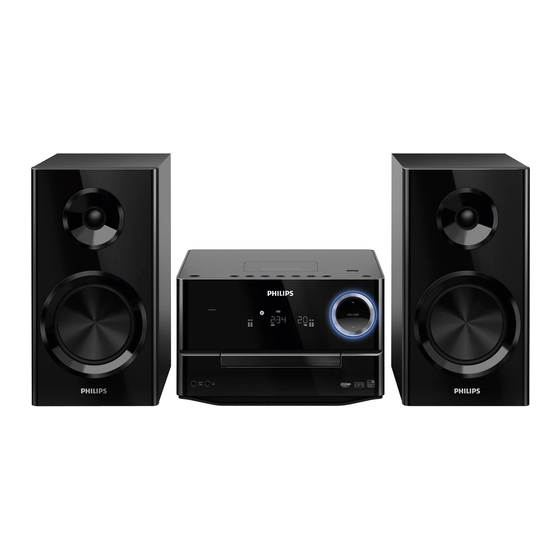
Philips MCM3000 Service Manual
120w micro music system
Hide thumbs
Also See for MCM3000:
- User manual (21 pages) ,
- Quick start manual (2 pages) ,
- Guía de inicio rápido (2 pages)
Advertisement
120W Micro music system
CONTENTS
Technical specification and version variation ...............................1
Service measurement setup..........................................................1-3
Service aids .................................................................................1-4
Instructions on CD playability ...............................................2-1.. 2-2
Block diagram ................................................................................3-1
Wiring diagram ..............................................................................4-1
Disassembly diagram..............................................................4-2..4-3
Main board
Circuit diagra......................................................................5-1..5-4
Layout diagram .........................................................................5-5
CD board
Circuit diagram .........................................................................6-1
Layout diagram .........................................................................6-2
DISPLAY/KEY/JACK/USB board
Circuit diagram .........................................................................7-1
Layout diagram ..................................................................7-2..7-3
SMPS Power board
Circuit diagram .........................................................................8-1
Layout diagram .........................................................................8-2
Exploded view diagram .................................................................9-1
©
Copyright 2011 Philips Consumer Electronics B.V. Eindhoven, The Netherlands
All rights reserved. No part of this publication may be reproduced, stored in a retrieval
system or transmitted, in any form or by any means, electronic, mechanical, photocopying,
or otherwise without the prior permission of Philips.
Published by SW 1116 Service Audio
Version 1.0
Subject to modification
MCM3000
/12/05
3141 785 36270
Advertisement
Table of Contents

Related Manuals for Philips MCM3000


Summary of Contents for Philips MCM3000
-
Page 1: Table Of Contents
Exploded view diagram ..............9-1 © Copyright 2011 Philips Consumer Electronics B.V. Eindhoven, The Netherlands All rights reserved. No part of this publication may be reproduced, stored in a retrieval system or transmitted, in any form or by any means, electronic, mechanical, photocopying, or otherwise without the prior permission of Philips. - Page 2 Description Pos. Description Pos. Battery location CABINET Dimensions with Boxes (L XXX x W XXX x H XXX): mm Material: XXX / XXX Dimensions without Boxes: XXX*XXX*XXX mm (LxWxH) Finishing: Weight (including packing): Unit in Mastercarton: Weight (excluding packing and batteries): XXXkg Units in Dealercarton: 1 set...
- Page 3 GENERAL DESCRIPTION CD PLAYER W/PLL RADIO AUX 2X60W LIFETIME(according to XUT-0026) 5 Years PERFORMANCE CLASSES Class Tuner Supply+Amplifier Loudspeaker Boxes Cassette Recorder DVD/CD SAFETY requirements IEC60065 RADIATION/IMMUNITY requirements(EMC) CLIMATIC requirements(according to UAN-D1590) till ℃ ALL climates +5℃ till ℃ MODERATE climates POWER SUPPLY MAINS (AC) Version...
- Page 4 SUPPLY + AF AMPLIFIER + LOUDSPEAKER (BOX SPECIFICATION) Audio Signal Processing LOUDNESS / S-BASS / PRESET EQUALIZER Use AUX as input source with following setup conditions : 1)Input sinewave 500mV at 1kHz to L/R channel of AUX-IN socket 2)Set preset equalizer to flat mode 3)Adjust volume to get 500 mW at 8 ohm load at L/R speaker outputs.
- Page 5 TECHNICAL DESCRIPTION 2X60W GENERAL PART Output Stage Protection: Temperature: Yes; INDICATORS VFD DISPLAY W/BACK-LIGHT Power Standby Mode: ELECTRICAL DATA DSC: Support Disc CD-DA CD-R/RW MP3 MAX: VEC: Level Difference: '+/-3 dB Tuner: FM 67.5 kHz Modulation. -6 dB track(Audio Disc 1 ,Trk 35) Ipod&Iphone: 500mW Aux :...
- Page 6 TECHNICAL DESCRIPTION DVD MINI SYSTEM GENERAL PART WAVE Range(-/21) TOLERANCE 87.5--108MHz AERIAL PIGTAIL ANTENNA WIRE 1.2M INDICATIORS ELECTRICAL DATA Nom limit Limit Unit unit -3dB Limiting Point : 17 23.5 Amplification Reserve(*1) Distortion(RF 1 mV, Freq.Dev.75kHz) : 18 26dB Quieting Sensitivty Crosstalk (RF 1mV Freq.
- Page 7 Description External DAC CD MECH: DA11VF Sanyo Channel Unbalance <±2dB ( Vol 0 ~ -50dB ) Frequency Response(+0.5/-1.0dB) 20Hz~20kHz Signal to Noise Ratio(A-weighted) 70dBA(Lim 65 dBA) THD Noise(20 ~20,000Hz) 0.5%(Lim 2%) (1kHz) 0.1% at -20dBFS Outband Attentuation 35dB Channel Separation 40dB (Lim.30dB) 35dB(Lim.25dB) 30dB(Lim.25dB)
- Page 8 TECHNICAL SPECIFICATION GENERAL PART Tmie Setting Clock and Timer Timer Wakeup Mode CD / Tuner/Aux (Depend on power off source) Remarks Time Setting 24 Hrs Wake Up Volume Control Volume at Wakeup No of Timer Settings Clock Accuracy Lim. +/- 2 sec / day RC operating distance INDICATORS Display Type...
- Page 9 MEASUREMENT SETUP Tuner FM Bandpass LF Voltmeter 250Hz-15kHz e.g. PM2534 e.g. 7122 707 48001 RF Generator e.g. PM5326 S/N and distortion meter e.g. Sound Technology ST1700B Use a bandpass filter to eliminate hum (50Hz, 100Hz) and disturbance from the pilottone (19kHz, 38kHz). Tuner AM (MW,LW) Bandpass LF Voltmeter...
-
Page 10: Service Aids
SERVICE AIDS WARNING All ICs and many other semi-conductors are susceptible to electrostatic discharges (ESD). Careless handling during repair can reduce life drastically. When repairing, make sure that you are connected with the same potential as the mass of the set via a wrist wrap with resistance. Keep components and tools also at this potential. -
Page 11: Instructions On Cd Playability
2 - 1 INSTRUCTIONS ON CD PLAYABILITY Customer complaint "CD related problem" Set remains closed! check playability playability ok ? For flap loaders (= access to CD drive possible) "fast" lens cleaning cleaning method is recommended check playability playability ok ? Play a CD for at least 10 minutes check playability... - Page 12 2 - 2 INSTRUCTIONS ON CD PLAYABILITY PLAYABILITY CHECK LIQUID LENS CLEANING Before touching the lens it is advised to clean the surface of the lens by blowing clean air over it. For sets which are compatible with CD-RW discs This to avoid that little particles make scratches on use CD-RW Printed Audio Disc ....7104 099 96611 the lens.
-
Page 13: Block Diagram
3 - 1 3 - 1 SET BLOCK DIAGRAM... -
Page 14: Wiring Diagram
4 - 1 4- 1 SET WIRING DIAGRAM... - Page 15 5 - 1 5 - 1 CIRCUIT DIAGRAM - MAIN BOARD PART 1 MCU3.3V C70 1 0.1uF R70 3 VC25 C A P _ N P C A P A C I T O R _ P O L TC70 5 P_CON 4.7UF R71 0...
- Page 16 5 - 2 5 - 2 CIRCUIT DIAGRAM - MAIN BOARD PART 2 +8VCC AUX JACK 2.2uF JK603 L3 FB300 4052_SET AUX-RIN AUX1 L7 FB300 2.2uF 2.2uF 2.2uF L4 FB300 R62 1K D2761 IC511 FB300 3P/2.0mm 2.2uF 2.2uF CN606 2.2uF +8VCC AUX2 FB300...
- Page 17 5 - 3 5 - 3 CIRCUIT DIAGARM - MAIN BOARD PART 3 VOL-CLK R427 Q401 7805 R406 1K EQ-SDA USB+5V LOV-TADA R421 EQ-SCL R405 1K 100PF IN5817 C427 D401 R116 EQ_ROUT R512 C429 AGND 5.6K AUX-L C428 FB300 R422 AGND U902 +5VCC...
- Page 18 5 - 4 5 - 4 CIRCUIT DIAGARM - MAIN BOARD PART 4 C341 0.1u L322 R320 OSC. VSSA. L310 33uH HR_CH+ 5.6k R318 HR_OUT IC314 R321 C373 8 RIN+ RIN+ 5.6k ROUT 16 ROUT. C347 9 RIN- RIN- 0.015 HR_CH- R340 C380...
- Page 19 5 - 5 5 - 5 LAYOUT DIAGRAM - MAIN BOARD...
-
Page 20: Circuit Diagra
6 - 1 6 - 1 CIRCUIT DIAGRAM - CD BOARD EC920 R959 220uF 2K/0603 LINE_R C929 R986 R979 C A P _ N P _ 5 3400pF/0603 1N4148/NC 10K/0603 DAC_R 10K/0603 D I O D E R _ 9 MUTE AMUTE AUD_GND... -
Page 21: Layout Diagram
6 - 2 6 - 2 LAYOUT DIAGRAM - CD BOARD... -
Page 22: Circuit Diagram
7 - 1 7 - 1 CIRCUIT DIAGRAM - DISPLAY/KEY/JACK/USB BOARD VFD701 OPEN R101 SW713 2.2K SOURCE IR701 RPM-7100 R100 POW ER 4.7K SW718 R390 LED702 IC701 UPD16311 AUDIO-DET 4052-DET IPOD-R LCD-CS RETURN LCD-RW IPOD-L LCD-DAT KEY2 DET13 R708B DET30 STANBY_ LED MOTO_ ON R112... -
Page 23: Layout Diagram
7 - 2 7 - 2 LAYOUT DIAGRAM - DISPLAY/KEY/JACK/USB BOARD TOP SIDE... -
Page 24: Layout Diagram
7 - 3 7 - 3 LAYOUT DIAGRAM - DISPLAY/KEY/JACK/USB BOARD BOTTOM... - Page 25 8 - 1 8 - 1 CIRCUIT DIAGRAM - SMPS POWER BOARD TO CN1101 AC101 FUSE1101 GBU406 LF1101 T5A L 250V 540UH 540UH 540UH NTC1 TO CN1102 SCK 055 SW-2 SW-1 +12V EL25 MBR10200 PWR-ON R230 1N4148 4N60 FR107 102/100V LN3C63 2.7K 0.1UF...
- Page 26 8 - 2 8 - 2 LAYOUT DIAGRAM - SMPS POWER BOARD...
-
Page 27: Exploded View Diagram
9 - 1 9 - 1 EXPLODED VIEW DIAGRAM...