Table of Contents
Advertisement
SERVICE MANUAL
Ver. 1.7 2014.06
• HBD-E2100 is the amplifi er, video, HDMI, BD/DVD/CD system, USB, LAN,
wireless LAN, Bluetooth, NFC and FM tuner section in BDV-E2100.
• HBD-E3100 is the amplifi er, video, HDMI, BD/DVD/CD system, USB, LAN,
wireless LAN, Bluetooth, NFC and FM tuner section in BDV-E3100.
• HBD-E3200 is the amplifier, video, HDMI, BD/DVD/CD system, USB, LAN,
wireless LAN, Bluetooth, NFC and FM tuner section in BDV-E3200.
• HBD-E4100 is the amplifi er, video, HDMI, BD/DVD/CD system, USB, LAN,
wireless LAN, Bluetooth, NFC and FM tuner section in BDV-E4100.
• HBD-E6100 is the amplifi er, video, HDMI, BD/DVD/CD system, USB, LAN,
wireless LAN, Bluetooth, NFC and FM tuner section in BDV-E6100.
Model Name Using Similar Mechanism
Mechanism Type
Optical Pick-up Block Name
Amplifi er Section
US model only:
AUDIO POWER SPECIFICATIONS
POWER OUTPUT AND TOTAL HARMONIC DISTORTION:
(FTC)
Front L + Front R:
With 3 ohms loads, both channels driven, from
180 Hz - 20,000 Hz;
rated 50 watts per channel
minimum RMS power, with no more than 1%
total harmonic distortion from 250 milliwatts to
rated output.
BDV-E6100/BDV-E4100/BDV-E3100/BDV-E3200
BDV-E2100 (Except UK model):
POWER OUTPUT (rated)
Front L/Front R:
75 W + 75 W (at 3 ohms, 1 kHz, 1% THD)
POWER OUTPUT (reference)
Front L/Front R/Surround L/Surround R:
125 W (per channel at 3 ohms, 1 kHz)
Center:
250 W (at 6 ohms, 1 kHz)
Subwoofer:
250 W (at 6 ohms, 80 Hz)
Inputs (Analog)
AUDIO IN
Sensitivity: 1 V/400 mV
MIC 1/2
Sensitivity: 10 mV (Singapore model)
Inputs (Digital)
TV (Audio Return Channel/OPTICAL)
Supported formats: LPCM 2CH
(up to 48 kHz), Dolby Digital, DTS
BDV-E2100 (UK model)
POWER OUTPUT (rated)
Front L/Front R:
75 W + 75 W (at 3 ohms, 1 kHz, 1% THD)
POWER OUTPUT (reference)
Front L/Front R/Surround L/Surround R:
100 W (per channel at 3 ohms, 1 kHz)
Center:
200 W (at 6 ohms, 1 kHz)
Subwoofer:
200 W (at 6 ohms, 80 Hz)
BDV-E4100/ BDV-E6100 (Chinese model)
POWER OUTPUT
Front L/Front R/Surround L/Surround R:
75 W (per channel at 3 ohms, 1 kHz)
9-890-611-08
Sony Corporation
2014F80-1
©
2014.06
Published by Sony EMCS (Malaysia) PG Tec
HBD-E2100/E3100/E3200/E4100/
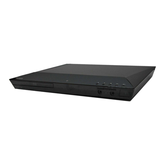
Photo: HBD-E3100
BDP-S3100
BPX-7
KEM480AAA
SPECIFICATIONS
Center:
150 W (at 6 ohms, 1 kHz)
Subwoofer:
150 W (at 6 ohms, 80 Hz)
Inputs (Analog)
AUDIO IN
Sensitivity: 1 V/400 mV
Inputs (Digital)
TV (Audio Return Channel/OPTICAL)
Supported formats: LPCM 2CH (up to 48 kHz),
Dolby Digital, DTS
HDMI Section
Connector
Type A (19 pin)
BD/DVD/CD System
Signal format system
NTSC/PAL (except US, PX and Canadian models)
NTSC (US, PX and Canadian models)
USB Section
(USB) port:
Type A (For connecting USB memory, memory
card reader, digital still camera, and digital video
camera)
LAN Section
LAN (100) terminal
100 BASE-TX Terminal
Wireless LAN Section
Standards Compliance
IEEE 802.11 b/g/n
Frequency and Channel
US, Canadian, Argentina and Taiwan models:
2.4 GHz band: channels 1–11
Other models:
2.4 GHz band: channels 1–13
Frequency band
2.4000 GHz - 2.4835 GHz
Canadian Model
Singapore Model
HBD-E2100/E3100/E4100/E6100
Taiwan Model
HBD-E2100/E4100/E6100
HBD-E2100/E3100/E4100
Chinese Model
HBD-E2100/E3100/E3200/E4100/E6100
Argentina Model
Australian Model
Russian Model
Saudi Arabia Model
HBD-E3100/E4100/E6100
South African Model
HBD-E2100/E3100/E6100
Bluetooth Section
Communication system Bluetooth Specification version 3.0
Output
Bluetooth Specification Power Class 2
Maximum communication range
Line of sight approx. 10 m
(except US, PX and Canadian models)
Line of sight approx. 10 m (33ft)
(US, PX and Canadian models)
Frequency band
2.4 GHz band
2.4000 GHz - 2.4835 GHz
Modulation method
FHSS (Freq Hopping Spread Spectrum)
Compatible Bluetooth profiles
A2DP 1.2 (Advanced Audio Distribution
Profile)
AVRCP 1.3 (Audio Video Remote Control
Profile)
Supported Codecs
3)
SBC
Transmission range (A2DP)
20 Hz – 20,000 Hz (Sampling frequency
44.1 kHz, 48 kHz)
1)
The actual range will vary depending on factors such as obstacles
between devices, magnetic fields around a microwave oven, static
electricity, cordless phone, reception sensitivity, antenna's perfor-
mance, operating system, software application, etc.
Bluetooth standard profiles indicate the purpose of Bluetooth
2)
communication between devices.
3)
Codec: Audio signal compression and conversion format
4)
Subband Codec
BLU-RAY DISC/DVD RECEIVER
E6100
US Model
HBD-E2100/E3100
AEP Model
UK Model
HBD-E4100/E6100
E Model
BDV-E2100/E4100
HBD-E2100/E6100
Thai Model
PX Model
HBD-E2100
1)
1)
2)
4)
, AAC
Advertisement
Table of Contents

Related Manuals for Sony HBD-E2100


Summary of Contents for Sony HBD-E2100
-
Page 1: Service Manual
Chinese Model Photo: HBD-E3100 HBD-E4100/E6100 E Model • HBD-E2100 is the amplifi er, video, HDMI, BD/DVD/CD system, USB, LAN, HBD-E2100/E3100/E3200/E4100/E6100 wireless LAN, Bluetooth, NFC and FM tuner section in BDV-E2100. Argentina Model • HBD-E3100 is the amplifi er, video, HDMI, BD/DVD/CD system, USB, LAN, wireless LAN, Bluetooth, NFC and FM tuner section in BDV-E3100. - Page 2 • The Bluetooth word mark and logos are registered trademarks owned by Bluetooth SIG, Inc. and any use of such marks by Sony Corporation is under license. Other trademarks and trade names are those of their respective owners. • MPEG Layer-3 audio coding technology and patents licensed from Fraunhofer IIS and Thomson.
- Page 3 HBD-E2100/E3100/ E3200/E4100/E6100 Ver. 1.5 SAFETY CHECK-OUT After correcting the original service problem, perform the follow- ing safety check before releasing the set to the customer: Check the antenna terminals, metal trim, “metallized” knobs, screws, and all other exposed metal parts for AC leakage.
-
Page 4: Table Of Contents
HBD-E2100/E3100/E3200/E4100/E6100 Ver. 1.5 TABLE OF CONTENTS SERVICING NOTES 6-19. Printed Wiring Board - PANEL Board - ......56 ..........6-20. Schematic Diagram - PANEL Board - ......57 6-21. Printed Wiring Board DISASSEMBLY - KARAOKE Board (SP, RU) - ........58 2-1. -
Page 5: Servicing Notes
HBD-E2100/E3100/E3200/E4100/E6100 Ver. 1.5 SECTION 1 SERVICING NOTES NOTE OF REPLACING THE IC101, IC102, IC103, NOTES ON HANDLING THE OPTICAL PICK-UP IC203, IC204, IC601, IC706, IC801 AND IC1001 ON BLOCK OR BASE UNIT THE MB1002 BOARD IC101, IC102, IC103, IC203, IC204, IC601, IC706, IC801 and The laser diode in the optical pick-up block may suffer electro- IC1001 on the MB1002 board cannot exchange with single. - Page 6 HBD-E2100/E3100/E3200/E4100/E6100 Ver. 1.5 NOTE REPLACING OPTICAL DEVICE 1-3. Barcode decoder (BDPRdec) (KEM480AAA) OR MB1002 BOARD Jig name : BDPRdec.exe Release : 2011.8.25 The password will be supplied to only service HQ, and Version : 3.0.0.0 service center name, q’ty and all of software registered...
- Page 7 HBD-E2100/E3100/E3200/E4100/E6100 Ver. 1.5 2. Pass-fail judgment of the optical device (KEM480AAA) Perform pass-fail judgment to judge whether the repair of the optical device (KEM480AAA) is necessary. 2-1. Flow of drive section check Confirm F201, F202, Confirm whether Confirm whether the...
- Page 8 HBD-E2100/E3100/E3200/E4100/E6100 Ver. 1.5 3. Optical device (KEM480AAA) replacement Flow of replacement: Note: The photo in fl ow is an image. Save the text data to USB memory Barcode label on (memory capacity new optical device need not be 8GB) (KEM480AAA)
- Page 9 HBD-E2100/E3100/E3200/E4100/E6100 Ver. 1.5 NOTE OF REPLACING MB1002 BOARD OR WLAN/ NOTE THE BD DRIVE (BPX-7) PARTS REPLACING BT COMBO CARD The mechanism blocks except optical device of BD drive (BPX-7) When the MB1002 board or WLAN/BT COMBO card are re- are chiefl...
- Page 10 HBD-E2100/E3100/E3200/E4100/E6100 Ver. 1.5 MODEL IDENTIFICATION NOTE OF REPLACING THE IC3102 AND IC3302 ON - Rear view - THE AMP BOARD AND THE COMPLETE AMP BOARD When IC3102 and IC3302 on the AMP board and the complete Part No. AMP board are replaced, it is necessary to spread the compound (GREASE (G-747)) 1KG) (Part No.
- Page 11 HBD-E2100/E3100/E3200/E4100/E6100 Ver. 1.5 CHECKING METHOD OF NETWORK OPERATION 2. Checking method of wired LAN operation It is necessary to check the network operation, when replacing the Check that access point is recognized surely. MB1002 board. Check the operation of wireless and wired LAN, according to the following method.
- Page 12 HBD-E2100/E3100/E3200/E4100/E6100 Ver. 1.7 HOW TO OPEN THE TRAY WHEN POWER SWITCH TURN OFF Note 1: After the case is removed, this work is done. Note 2: Please prepare the thin wire (clip etc. processed to the length of 8 cm or more).
-
Page 13: Disassembly
HBD-E2100/E3100/E3200/E4100/E6100 Ver. 1.5 SECTION 2 DISASSEMBLY • This set can be disassembled in the order shown below. 2-1. DISASSEMBLY FLOW 2-2. HOW TO BEND FFC (Page 14) 2-3. CASE (Page 15) 2-4. PANEL LOADING ASSY (Page 15) 2-5. FRONT PANEL ASSY (Page 16) 2-6. -
Page 14: How To Bend Ffc
HBD-E2100/E3100/E3200/E4100/E6100 Ver. 1.5 2-2. HOW TO BEND FFC : Mountain fold : Valley fold wire (flat type) (8 core), length 260 mm (Ref. No. 52) 40 mm 220 mm RC-S801/A MB1002 45º (WW) (CN806) The upper side The upper side is contact side. -
Page 15: Case
HBD-E2100/E3100/E3200/E4100/E6100 Ver. 1.5 Note: Follow the disassembly procedure in the numerical order given. 2-3. CASE 1 four screws (+BV3 (3-CR)) 7 case 3 five claws 2 four screws (+BV3 (3-CR)) 2-4. PANEL LOADING ASSY 4 panel loading assy hole –... -
Page 16: Front Panel Assy
HBD-E2100/E3100/E3200/E4100/E6100 Ver. 1.5 2-5. FRONT PANEL ASSY • Abbreviation : Russian model switching regulator (SWR1) : Singapore model MB1002 board front side 1 wire (flat type) (8 core) (CN806) (E2100) (E3100/E4100/E6100) 3 three claws 3 three claws 4 front panel assy... -
Page 17: Power Key Board, Wlan/Bt Combo Card, Karaoke Board (Sp, Ru), Panel Board
HBD-E2100/E3100/E3200/E4100/E6100 Ver. 1.5 2-7. POWER KEY BOARD, WLAN/BT COMBO CARD, KARAOKE BOARD (SP, RU), PANEL BOARD switching regulator (SWR1) front side MB1002 board front side harness USB MB1002 board 7 wire (flat type) (21 core) (CN01) (SP, RU) wire (flat type) (15 core) (CN02) -
Page 18: Mb1002 Board
HBD-E2100/E3100/E3200/E4100/E6100 Ver. 1.5 2-8. MB1002 BOARD 5 five screws (+BV3 (3-CR)) 8 MB1002 board 6 one screw (+BV3 (3-CR)) 7 one screw (+B 3 1 CN201 (2P) 2 tape 3 wire (flat type) (24 core) (CN707) 4 CN202 (8P) 2-9. -
Page 19: Switching Regulator (Swr1)
HBD-E2100/E3100/E3200/E4100/E6100 Ver. 1.7 2-10. SWITCHING REGULATOR (SWR1) 2 five screws (+BV3 (3-CR)) 5 switching regulator (SWR1) (3L392W-1) (US, CND, AEP, UK, SAF, SP, TW, AUS, TH, CH) (3L392W) (E3, E51, PX, EA, E12, E32, RU, MX6, AR) 3 four claws... -
Page 20: Optical Pick-Up Block (Kem480Aaa), Wire (Flat Type)
HBD-E2100/E3100/E3200/E4100/E6100 Ver. 1.5 2-11. OPTICAL PICK-UP BLOCK (KEM480AAA), WIRE (FLAT TYPE) 3 holder, chuck assy (T) 1 four claws 2 two claws 0 insulator 6 two screws (S), float qa device, optical KEM480AAA qs tape, non-halogene qf tape, FFC qg flexible flat cable... -
Page 21: Test Mode
HBD-E2100/E3100/E3200/E4100/E6100 Ver. 1.5 SECTION 3 TEST MODE COLD RESET FACTORY INITIALIZE The cold reset clears certain data in this system without initialize Return all of the unit setting to their factory defaults. Note 1: Disconnect the following connections when you use this mode. - Page 22 HBD-E2100/E3100/E3200/E4100/E6100 Ver. 1.5 BD SERVICE MODE 6. The message “Close” appears, and press the [ ] button on the remote commander. Note: The operation in this mode must use a remote commander and TV monitor. Initialize Personal Information Setting method of the BD service mode: 1.
-
Page 23: Menu Tree
HBD-E2100/E3100/E3200/E4100/E6100 Ver. 1.5 2. Menu Tree Service Device Test Service [1] Dia [1] Dia [2] Lo [2] Lo [3] Factory Initialize [3] Factory Initialize [4] Network [4] Network [5] Version Up Video Test [5] Version Up [6] System Information [6] System Information... - Page 24 HBD-E2100/E3100/E3200/E4100/E6100 Ver. 1.5 3. Service Mode Menu (Top Menu) This is the top menu of service mode. Diag Each function is accessed from this screen. Device Test Category: Operation: Moves to Diag screen Diag Moves to Log screen Moves to Factory Initialize screen...
- Page 25 HBD-E2100/E3100/E3200/E4100/E6100 Ver. 1.5 6. Diag (Audio Input Test) 7. Diag (Wireless LAN Test) This screen performs audio input test. This screen performs wireless LAN test. Screen 1: Select Audio Input Test Category Screen 1: Selects the Wireless LAN test category...
- Page 26 CERT : NO-ENCRYPT [M]/[m] Selects Device WEPKEY : abcdef1234 Activate and Start Test : ABCDE12345 SSID : SONY-Test-R [RETURN] Returns to the selection of test category IPADDR : 192.168.1.100 NETMASK: 255.255.255.0 Screen 2: Select [1] Bluetooth Enable BROADCAST : 192.168.1.10 •...
- Page 27 HBD-E2100/E3100/E3200/E4100/E6100 Ver. 1.5 12. Log: Error Log (Output of each Log) (Screen 1) This screen displays the contents of each log. Diag Note: Do not refer to the displayed date. Category: Bluetooth Device Test Screen 1: Selects log Operation: Diag...
- Page 28 HBD-E2100/E3100/E3200/E4100/E6100 Ver. 1.5 13. Factory Initialize (Factory Settings) 15. Network (Network Test Diagnosis Screen: Ping) Ping test for the wired ethernet. There is a possibility that this mode cannot be correctly execut- ed. Never use this mode. Screen 1: Ping Test Operation: 14.
- Page 29 HBD-E2100/E3100/E3200/E4100/E6100 Ver. 1.5 16. Version Up Test (Disc Update) (Screen 5) This screen performs version update test. Software Update Operation: Software update has started. ]/[ ] Activate the selected category. Never turn off while performing update. [RETURN] Return to Service Top Menu.
- Page 30 HBD-E2100/E3100/E3200/E4100/E6100 Ver. 1.5 (Screen 1) Drive System Information [1] Drive OP data Write Main LSIname: Model: Destination: Drive OP data Write Sequence Number: MAC: Insert USB StorageDevice ... Remove DISC and Close tray. IF-con Block0 Version: Bootloader Version: Disc : Load...
- Page 31 HBD-E2100/E3100/E3200/E4100/E6100 Ver. 1.5 CONFIRMATION ITEM 2. Networking Confi rmation 1. Playback Operation Confi rmation Confi rm it according to the following procedure when you confi rm 1-1. Test Disc the connection of the network. Note: Do not execute “Network Connection Diagnostics” of “Network Part No.
-
Page 32: Electrical Check
HBD-E2100/E3100/E3200/E4100/E6100 Ver. 1.5 SECTION 4 ELECTRICAL CHECK FM AUTO STOP CHECK generator Procedure: 1. Turn the power on. 2. Input the following signal from Signal Generator to FM an- tenna input directly. Carrier frequency : A = 87.5 MHz, B = 98 MHz, C = 108 MHz... -
Page 33: Troubleshooting
HBD-E2100/E3100/E3200/E4100/E6100 Ver. 1.5 SECTION 5 TROUBLESHOOTING... - Page 34 HBD-E2100/E3100/E3200/E4100/E6100 Ver. 1.5...
- Page 35 HBD-E2100/E3100/E3200/E4100/E6100 Ver. 1.5...
-
Page 36: Diagrams
HBD-E2100/E3100/E3200/E4100/E6100 Ver. 1.7 SECTION 6 DIAGRAMS • Circuit Boards Location MB1002 board RC-S801/A (WW) AMP board POWER KEY board card, WLAN/BT COMBO PANEL board switching regulator (SWR1) (3L392W-1) (US, CND, AEP, UK, SAF, SP, TW, AUS, TH, CH) KARAOKE board (SP, RU) -
Page 37: Block Diagram - Servo Section
HBD-E2100/E3100/E3200/E4100/E6100 Ver. 1.5 6-1. BLOCK DIAGRAM - SERVO Section - BD DECODER IC101 (1/3) CN501 (1/2) RFIP RFIN FRONT USB VBUS IC406 VOUT DCDC5V CN52 SDIO FECFREQ SCLK FEOSCEN USB_DP_P1 P56 USB_DM_P1 P55 SEN_LDD FECMOD TEST_V P256 FPDODVD VC_PD HAVC... -
Page 38: Block Diagram - Memory/Hdmi Section
HBD-E2100/E3100/E3200/E4100/E6100 Ver. 1.5 6-2. BLOCK DIAGRAM - MEMORY/HDMI Section - BD DECODER IC101 (2/3) SD-RAM SD-RAM IC102 IC103 DQL0 - DQL7, DQL0 - DQL7, RDQ0 - RDQ15 RDQ16 - RDQ31 DQU0 - DQU7 DQU0 - DQU7 D0A0 - D0A13 D0A0 - D0A13... -
Page 39: Block Diagram - Main Section
HBD-E2100/E3100/E3200/E4100/E6100 Ver. 1.5 6-3. BLOCK DIAGRAM - MAIN Section - MEMORY/HDMI SECTION (Page 38) BD DECODER IC101 (3/3) MIC 1 IC71 OPTICAL RECEIVER DIGITAL IN P246 AOSDATA3 JACK OPTICAL IC701 MIC 2 ELECTRICAL VOLUME IC72 A/D CONVERTER IC704 SP, RU... -
Page 40: Block Diagram - Amp Section
HBD-E2100/E3100/E3200/E4100/E6100 Ver. 1.5 6-4. BLOCK DIAGRAM - AMP Section - POWER AMP STREAM PROCESSOR IC3102 IC3001 TB3451 AMP_MCK PWM_P_1 11 MCLK 29 1N1A OUT1A FRONT L PWM_M_2 AMP_LRCK 22 LRCK IN1B OUT1A MAIN AMP_BCK 23 SCLK PWM_M_8 IN2A SECTION OVERLOAD... -
Page 41: Block Diagram - Power Supply Section
HBD-E2100/E3100/E3200/E4100/E6100 Ver. 1.5 6-5. BLOCK DIAGRAM - POWER SUPPLY Section - SWR1 DCDC5V SWITCHING REGULATOR 5V VOLTAGE CONTROL DC-DC CONVERTER Q206 IC205 F202 FE_SW5V 3 SW UNSW12V OVERLOAD DETECTION Q207 12V VOLTAGE CONTROL Q205 F203 FE_SW12V FEUNSW12V OVERLOAD DETECTION Q202 3.3V VOLTAGE... - Page 42 HBD-E2100/E3100/E3200/E4100/E6100 Ver. 1.7 THIS NOTE IS COMMON FOR PRINTED WIRING BOARDS AND SCHEMATIC DIAGRAMS. • Waveforms (In addition to this, the necessary note is printed in each block.) – MB1002 Board – For Printed Wiring Boards. For Schematic Diagrams. Note:...
-
Page 43: Mb1002 Board (Component Side)
HBD-E2100/E3100/E3200/E4100/E6100 Ver. 1.5 6-6. PRINTED WIRING BOARD - MB1002 Board (Component Side) - • See page 36 for Circuit Boards Location. • : Uses unleaded solder. J702 MB1002 BOARD AUDIO IN (COMPONENT SIDE) CN401 CN706 CN380 HDMI DIGITAL IN LAN (100) -
Page 44: Printed Wiring Board - Mb1002 Board (Conductor Side)
HBD-E2100/E3100/E3200/E4100/E6100 Ver. 1.5 6-7. PRINTED WIRING BOARD - MB1002 Board (Conductor Side) - • See page 36 for Circuit Boards Location. • : Uses unleaded solder. MB1002 BOARD (CONDUCTOR SIDE) JL714 JL715 CL714 CL713 R455 D202 R412 C409 Q208 R406... -
Page 45: Schematic Diagram - Mb1002 Board (1/6)
HBD-E2100/E3100/E3200/E4100/E6100 Ver. 1.5 6-8. SCHEMATIC DIAGRAM - MB1002 Board (1/6) - • See page 59 for IC Block Diagrams. • See page 64 for IC Pin Function Descriptions. MB1002 BOARD (1/6) NFD7 D0DQ0 JL1001 NFD7 RDQ0 NFD6 JL1002 P107 JL198... -
Page 46: Schematic Diagram - Mb1002 Board (2/6)
HBD-E2100/E3100/E3200/E4100/E6100 Ver. 1.5 6-9. SCHEMATIC DIAGRAM - MB1002 Board (2/6) - MB1002 BOARD (2/6) MB1002 BOARD IC201 (3/6) BD00GA3WEFJ-E2 DCDC5V IC201 (Page 47) DC FAN DRIVER CN201 JL218 DC-FAN + JL219 DC-FAN - FE_SW12V MB1002 (FAN) L205 C242 D202 R249... -
Page 47: Schematic Diagram - Mb1002 Board (3/6)
HBD-E2100/E3100/E3200/E4100/E6100 Ver. 1.5 6-10. SCHEMATIC DIAGRAM - MB1002 Board (3/6) - • See page 59 for IC Block Diagrams. • See page 64 for IC Pin Function Descriptions. MB1002 BOARD (3/6) CORE_1.2V IC101 (2/3) UNSW5.5V CXD90019R-BA IC101 MB1002 IC408 BD DECODER... -
Page 48: Schematic Diagram - Mb1002 Board (4/6)
HBD-E2100/E3100/E3200/E4100/E6100 Ver. 1.5 6-11. SCHEMATIC DIAGRAM - MB1002 Board (4/6) - • See page 59 for IC Block Diagrams. • See page 64 for IC Pin Function Descriptions. MB1002 BOARD (4/6) CN660 FE_SLED_A- CL661 FE_SLED_A+ CL662 FE_SLED_B- CL663 FE_SLED_B+ R522... -
Page 49: Schematic Diagram - Mb1002 Board (5/6)
HBD-E2100/E3100/E3200/E4100/E6100 Ver. 1.5 6-12. SCHEMATIC DIAGRAM - MB1002 Board (5/6) - • See page 42 for Waveforms. • See page 59 for IC Block Diagrams. MB1002 BOARD (5/6) STA516_TH_WARN STA516_TH_WARN TAS5538_XPDN TAS5538_XPDN MB1002 DRIVER_SD/PVDD_DETECT DRIVER_SD/PVDD_DETECT DC_DET BOARD DC_DET (6/6) L707... -
Page 50: Schematic Diagram - Mb1002 Board (6/6)
HBD-E2100/E3100/E3200/E4100/E6100 Ver. 1.5 6-13. SCHEMATIC DIAGRAM - MB1002 Board (6/6) - • See page 42 for Waveforms. • See page 64 for IC Pin Function Descriptions. MB1002 BOARD (6/6) MB1002 BOARD NAND_RESET NAND_RESET (1/6) (Page 45) PCONT_STA516 I2C_DATA_TUNER I2C_DATA_TUNER TAS5538_XPDN... -
Page 51: Printed Wiring Board - Amp Board (Component Side)
HBD-E2100/E3100/E3200/E4100/E6100 Ver. 1.5 6-14. PRINTED WIRING BOARD - AMP Board (Component Side) - • See page 36 for Circuit Boards Location. • : Uses unleaded solder. SPEAKERS TB3401 TB3451 SUR L SUR R CENTER SUBWOOFER FRONT L FRONT R AMP BOARD –... -
Page 52: Printed Wiring Board - Amp Board (Conductor Side)
HBD-E2100/E3100/E3200/E4100/E6100 Ver. 1.5 6-15. PRINTED WIRING BOARD - AMP Board (Conductor Side) - • See page 36 for Circuit Boards Location. • : Uses unleaded solder. AMP BOARD (CONDUCTOR SIDE) JL3470 JL3469 JL3412 JL3411 JL3407 JL3466 JL3461 JL3459 C3451 C3460... -
Page 53: Schematic Diagram - Amp Board (1/3)
HBD-E2100/E3100/E3200/E4100/E6100 Ver. 1.5 6-16. SCHEMATIC DIAGRAM - AMP Board (1/3) - • See page 59 for IC Block Diagrams. AMP BOARD (1/3) DRIVE_SD DC_DET CN3505 TP3001 JL3001 D3.3V TAS5538_SCL TP3002 JL3002 TAS5538_SCL TP3004 JL3004 RB3001 TAS5538_SDA D3.3V TP3007 JL3007 TAS5538_XPDN... -
Page 54: Schematic Diagram - Amp Board (2/3)
HBD-E2100/E3100/E3200/E4100/E6100 Ver. 1.5 6-17. SCHEMATIC DIAGRAM - AMP Board (2/3) - • See page 59 for IC Block Diagrams. AMP BOARD (2/3) DC_DET JL3501 SL3001 PVDD_DET JL3503 R3555 D3503 RB751S40, 115 SL3002 C3552 47 4V C3570 SL3000 R3556 C3554 0.01... -
Page 55: Schematic Diagram - Amp Board (3/3)
HBD-E2100/E3100/E3200/E4100/E6100 Ver. 1.5 6-18. SCHEMATIC DIAGRAM - AMP Board (3/3) - • See page 59 for IC Block Diagrams. AMP BOARD (2/3) (Page 54) 20 21 AMP BOARD (3/3) Q3202 HN1A01FU OVERLOAD JL3213 DETECTION C3228 R3212 100k JL3212 RB3304 100k... -
Page 56: 6-19. Printed Wiring Board - Panel Board
HBD-E2100/E3100/E3200/E4100/E6100 Ver. 1.5 6-19. PRINTED WIRING BOARD - PANEL Board - • See page 36 for Circuit Boards Location. • : Uses unleaded solder. MB1002 MB1002 BOARD BOARD CN803 CN805 KARAOKE (Page 43) (Page 43) BOARD SP, RU CN01 CN71... -
Page 57: 6-20. Schematic Diagram - Panel Board
HBD-E2100/E3100/E3200/E4100/E6100 Ver. 1.5 6-20. SCHEMATIC DIAGRAM - PANEL Board - PANEL BOARD CL16 ND01 VACUUM FLUORESCENT DISPLAY IC03 MM3411Z41URE IC01 IC03 GP1UE27XK0VF IC01 +3.3V REG REMOTE CONTROL SIGNAL RECEIVER 15 16 17 18 19 20 21 22 23 24 25... -
Page 58: Printed Wiring Board - Karaoke Board (Sp, Ru)
HBD-E2100/E3100/E3200/E4100/E6100 Ver. 1.5 6-21. PRINTED WIRING BOARD – KARAOKE Board (SP, RU) – 6-23. PRINTED WIRING BOARD – POWER KEY Board – • • • See page 36 for Circuit Boards Location. : Uses unleaded solder. • See page 36 for Circuit Boards Location. - Page 59 HBD-E2100/E3100/E3200/E4100/E6100 Ver. 1.5 • IC Block Diagrams IC3001 TAS5538DGGR (AMP BOARD (1/3)) PWM_HPM_L PWM_HPP_L 56 PWM_P_6 PWM_HPM_R 55 PWM_M_6 PWM_HPP_R 54 PWM_P_5 AVSS 53 PWM_M_5 PLL_FLTM 52 VR_PWM Power Supply PLL_FLTP 51 AVSS_PWM VR_ANA 50 AVDD_PWM Digital Audio Processor PWM Section...
- Page 60 HBD-E2100/E3100/E3200/E4100/E6100 Ver. 1.5 IC403 TC7WHU04FK (MB1002 BOARD (3/6)) 4 GND 3 2A 2 3Y 1 1A IC406 TPS2065CDBVR (MB1002 BOARD (3/6)) Current Sense 1 OUT Charge Current 2 GND (Disabled+ Pump Limit UVLO) Driver 3 FLT UVLO OTSD 9-ms Deglitch...
- Page 61 HBD-E2100/E3100/E3200/E4100/E6100 Ver. 1.5 IC601 TPIC2060ADFDRG4 (MB1002 BOARD (4/6)) 56 NC LINFB GPOUT LIN9VG TEST int 10V Regulator SPM_RCOM AGND Charge XSLEEP pump MCOM SPM_ENA SIOV Current limit SPM Logic BEMF DAC PWM PGND_SPM2 detector XSLEEP pwr FET -driver Digital core...
- Page 62 HBD-E2100/E3100/E3200/E4100/E6100 Ver. 1.5 IC703 SN74LV4052APWR (MB1002 BOARD (5/6)) 2-COM 1-COM IC704 PCM1808PWR (MB1002 BOARD (5/6)) ANTIALIAS VINR LOW-PASS FILTER ANTIALIAS VINL LOW-PASS FILTER DELTA-SIGMA MODULATOR 1/64 SERIAL DECIMATION INTERFACE FILTER VREF 1 REFERENCE & WITH MODE/FORMAT DOUT HIGH-PASS CONTROL DELTA-SIGMA...
- Page 63 HBD-E2100/E3100/E3200/E4100/E6100 Ver. 1.5 IC706 RN5B701-0002 (MB1002 BOARD (5/6)) (AEP and UK models) IISD IISD Digital Signal Processing LOUT Filter LRCK/LOUT Digital Stereo Mixer Demodulator Decoder FRF1 1 BCLK/ROUT FM LNA ROUT RSSI Digital FRF2 2 Calculation Decoder LRCK Image Station...
- Page 64 HBD-E2100/E3100/E3200/E4100/E6100 Ver. 1.5 • IC Pin Function Descriptions MB1002 BOARD (1/6), (3/6), (4/6) IC101 CXD90019R-BA (BD DECODER) Pin No. Pin Name Description TRINB Input of Tracking Signal (B) TRINA Input of Tracking Signal (A) HAVC Decoupling Pin for Reference Voltage of Main and Sub Beams AVDD33_1 3.3 V Power Pin...
- Page 65 HBD-E2100/E3100/E3200/E4100/E6100 Ver. 1.5 Pin No. Pin Name Description LDD serial interface data. The pin is spike-free at power-on stage. FEGIO0 The pin is not allowed to pull-up in circuit layout. General IO FEGIO1 PC RS232 serial receive data. The pin is spike-free at power-on stage.
- Page 66 HBD-E2100/E3100/E3200/E4100/E6100 Ver. 1.5 Pin No. Pin Name Description RDQM1 Memory data mask bit 1 DDRVCCK_2 1.2V Digital Power DDRVREF Memory VREF RDQS0 Memory positive data strobe bit 0 RDQS0_ Memory negative data strobe bit 0 DDRVCCIO_2 1.5V Digital IO power...
- Page 67 HBD-E2100/E3100/E3200/E4100/E6100 Ver. 1.5 Pin No. Pin Name Description P144 RDQ20 Memory data bit 20 P145 RDQ22 Memory data bit 22 P146 RDQ18 Memory data bit 18 P147 DDRVCCIO_8 1.5V Digital IO power P148 RDQ16 Memory data bit 16 P149 RDQ27...
- Page 68 HBD-E2100/E3100/E3200/E4100/E6100 Ver. 1.5 Pin No. Pin Name Description Reserved for debug-only Uart pins. P195 UARXD (1) 1st RS232 RX (2) T8032 RS232 RX P196 AMUTE UPG_STATUS P197 HTPLG HDMI Hot Plug P198 DVCC33_IO_STB_2 3.3V Digital IO Power for Stand-By Module...
- Page 69 HBD-E2100/E3100/E3200/E4100/E6100 Ver. 1.5 Pin No. Pin Name Description P247 SPDIF SPDIF digital audio output P248 DVCC12_K_7 1.2V Digital Power P249 AVDD12_1 1.2 V Power Pin P250 RSTI Front-End Power on reset P251 VDAC0 Output of General DAC P252 VWDC2O Output Voltage 2 of Laser Diode Control in APC...
- Page 70 HBD-E2100/E3100/E3200/E4100/E6100 Ver. 1.5 MB1002 BOARD (1/6) IC102, IC103 K4B2G1646Q-BCMA (SD-RAM) Pin No. Pin Name Description VDDQ DQ Power Supply: 1.5V +/-0.075V DQU5 Data Input/output: Bi-directional data bus. DQU7 Data Input/output: Bi-directional data bus. NO_USE Not used NO_USE Not used NO_USE...
- Page 71 HBD-E2100/E3100/E3200/E4100/E6100 Ver. 1.5 Pin No. Pin Name Description Input Data Mask: DM is an input mask signal for write data. Input data is masked when DM is sampled HIGH coincident with that input data during a Write access. DM is sampled on both edges of DQS.
- Page 72 HBD-E2100/E3100/E3200/E4100/E6100 Ver. 1.5 Pin No. Pin Name Description Command Input: CAS (along with CS) defi ne the command being entered. NO_USE Not used NO_USE Not used NO_USE Not used Clock: CK is differential clock input. All address and control input signals are sampled on the crossing of the negative edge of CK.
- Page 73 HBD-E2100/E3100/E3200/E4100/E6100 Ver. 1.5 Pin No. Pin Name Description Bank Address Inputs: BA1 defi ne to which bank an Active, Read, Write or Precharge com- mand is being applied. Bank address also determines if the mode register or extended mode register is to be accessed during a MRS cycle.
- Page 74 HBD-E2100/E3100/E3200/E4100/E6100 Ver. 1.5 MB1002 BOARD (6/6) IC801 R5F3650KCDFB (SYSTEM CONTROLLER) Pin No. Pin Name Description SIRCS_IN SIRCS signal input from the remote control receiver Fan motor speed control signal output terminal control by DA converter FAN_CONT Port output higher, speed slower FL_DOUT Serial data output to the fl...
- Page 75 HBD-E2100/E3100/E3200/E4100/E6100 Ver. 1.5 Pin No. Pin Name Description STA516_XPDN DAMP Driver Standby Control TAS5538_XRST Reset signal output to the DAMP processor "L": reset TAS5538_XMUTE Muting on/off control signal output to DAMP processor "L": muting on NO_USE No used NO_USE No used...
-
Page 76: Exploded Views
HBD-E2100/E3100/E3200/E4100/E6100 Ver. 1.7 SECTION 7 EXPLODED VIEWS Note: • -XX and -X mean standardized parts, so : 110 – 240 V AC area in E model The components identifi ed by mark 9 con- they may have some difference from the : Chilean and Peruvian models tain confi... -
Page 77: Front Panel Section
HBD-E2100/E3100/E3200/E4100/E6100 Ver. 1.7 7-2. FRONT PANEL SECTION (E2100) not supplied BD drive section (BPX-7) (SP) (E3100/E4100/E6100) (SP, RU) not supplied not supplied (POWER KEY board) chassis bottom section (SP, RU ) (EXCEPT SP, RU) not supplied ND01 not supplied (NON-KARAOKE board) Note 2: Wires (fl... -
Page 78: Chassis Bottom Section
HBD-E2100/E3100/E3200/E4100/E6100 Ver. 1.7 7-3. CHASSIS BOTTOM SECTION not supplied (PX, MX6, E32) (E2100: SP for Hong Kong model) chassis section Note: Wires (fl at type) for service is all straight. Please bend it referring go “HOW TO BEND FFC” on page 14 when you install it in the unit. - Page 79 HBD-E2100/E3100/E3200/E4100/E6100 Ver. 1.7 Ref. No. Part No. Description Remark 9 102 A-1902-260-A MB1002 BOARD, COMPLETE (for SERVICE) (E6100: CND) 9 102 A-1902-269-A MB1002 BOARD, COMPLETE (for SERVICE) (E6100: AEP) 9 102 A-1902-276-A MB1002 BOARD, COMPLETE (for SERVICE) (E6100: RU) 9 102...
-
Page 80: Chassis Section
HBD-E2100/E3100/E3200/E4100/E6100 Ver. 1.7 7-4. CHASSIS SECTION SWR1 not supplied not supplied not supplied Ref. No. Part No. Description Remark 3-077-331-71 +BV3 (3-CR) 4-295-590-01 FOOT 0 M1 1-855-244-11 DC FAN 0 SWR1 1-798-453-11 SWITCHING REGULATOR (3L392W-1) (US, CND, AEP, UK, SAF, SP, TW, AUS, TH, CH) -
Page 81: Bd Drive Section (Bpx-7)
HBD-E2100/E3100/E3200/E4100/E6100 Ver. 1.5 7-5. BD DRIVE SECTION (BPX-7) not supplied not supplied not supplied supplied not supplied Note: Wires (fl at type) for service is all straight. Please bend it referring go “HOW TO BEND FFC” on page 14 when you install it in the unit. -
Page 82: Electrical Parts List
HBD-E2100/E3100/E3200/E4100/E6100 Ver. 1.7 SECTION 8 ELECTRICAL PARTS LIST Note: • Due to standardization, replacements in • SEMICONDUCTORS The components identifi ed by mark 0 the parts list may be different from the In each case, u: μ, for example: or dotted line with mark 0 are critical for parts specifi... - Page 83 HBD-E2100/E3100/E3200/E4100/E6100 Ver. 1.5 Ref. No. Part No. Description Remark Ref. No. Part No. Description Remark C3328 1-116-731-11 CERAMIC CHIP 2.2uF 6.3V D3103 6-503-967-01 DI STPS1H100A C3331 1-116-717-11 CERAMIC CHIP 10uF D3104 6-503-967-01 DI STPS1H100A C3333 1-116-717-11 CERAMIC CHIP 10uF D3105...
- Page 84 HBD-E2100/E3100/E3200/E4100/E6100 Ver. 1.5 KARAOKE MB1002 Ref. No. Part No. Description Remark Ref. No. Part No. Description Remark R3212 1-218-977-11 METAL CHIP 100K 1/16W 1-118-290-11 CERAMIC CHIP 0.001uF R3271 1-218-282-11 METAL CHIP 1/2W * C84 1-118-360-11 CERAMIC CHIP 0.1uF R3272 1-218-282-11...
- Page 85 HBD-E2100/E3100/E3200/E4100/E6100 Ver. 1.7 MB1002 Ref. No. Part No. Description Remark Ref. No. Part No. Description Remark A-1901-538-A MB1002 BOARD, COMPLETE (for SERVICE) A-1921-463-A MB1002 BOARD, COMPLETE (for SERVICE) (E2100: E51, MX6) (E2100: PX) A-1901-565-A MB1002 BOARD, COMPLETE (for SERVICE) A-1943-338-A...
- Page 86 HBD-E2100/E3100/E3200/E4100/E6100 Ver. 1.7 MB1002 Ref. No. Part No. Description Remark Ref. No. Part No. Description Remark C190 1-164-874-11 CERAMIC CHIP 100PF C327 1-165-908-11 CERAMIC CHIP 1uF C191 1-164-874-11 CERAMIC CHIP 100PF C328 1-165-908-11 CERAMIC CHIP 1uF C192 1-164-874-11 CERAMIC CHIP 100PF...
- Page 87 HBD-E2100/E3100/E3200/E4100/E6100 Ver. 1.7 MB1002 Ref. No. Part No. Description Remark Ref. No. Part No. Description Remark C601 1-116-716-11 CERAMIC CHIP 10uF C806 1-118-386-11 CERAMIC CHIP 0.1uF C603 1-116-734-11 CERAMIC CHIP 1uF C607 1-118-386-11 CERAMIC CHIP 0.1uF C807 1-118-386-11 CERAMIC CHIP 0.1uF...
- Page 88 HBD-E2100/E3100/E3200/E4100/E6100 Ver. 1.7 MB1002 Ref. No. Part No. Description Remark Ref. No. Part No. Description Remark IC201 6-716-462-01 IC BD00GA3WEFJ-E2 < RESISTOR > IC203 (Not supplied) IC TPS54295PWPR 0 R101 1-208-683-11 METAL CHIP 0.5% 1/16W IC204 (Not supplied) IC TPS54295PWPR...
- Page 89 HBD-E2100/E3100/E3200/E4100/E6100 Ver. 1.7 MB1002 Ref. No. Part No. Description Remark Ref. No. Part No. Description Remark R318 1-218-965-11 METAL CHIP 1/16W R726 1-218-973-11 METAL CHIP 1/16W R727 1-218-973-11 METAL CHIP 1/16W R319 1-218-941-81 METAL CHIP 1/16W R733 1-218-971-81 METAL CHIP...
- Page 90 HBD-E2100/E3100/E3200/E4100/E6100 Ver. 1.7 MB1002 PANEL Ref. No. Part No. Description Remark Ref. No. Part No. Description Remark R828 1-218-977-11 METAL CHIP 100K 1/16W R1010 1-218-965-11 METAL CHIP 1/16W R830 1-218-941-81 METAL CHIP 1/16W R7014 1-218-990-81 SHORT CHIP R831 1-218-957-11 METAL CHIP 2.2K...
- Page 91 HBD-E2100/E3100/E3200/E4100/E6100 Ver. 1.7 PANEL POWER KEY Ref. No. Part No. Description Remark Ref. No. Part No. Description Remark CN51 1-564-721-11 PIN, CONNECTOR (SMALL TYPE) 5P 1-216-813-11 METAL CHIP 1/10W CN52 1-819-866-11 USB CONNECTOR (A) ( ) 1-216-833-11 METAL CHIP 1/10W <...
- Page 92 HBD-E2100/E3100/E3200/E4100/E6100 Ver. 1.7 Ref. No. Part No. Description Remark 0 SWR1 1-798-453-21 SWITCHING REGULATOR (3L392W) (E3, E51, PX, EA, E12, E32, RU, MX6, AR)
-
Page 93: Revision History
Date Description of Revision 2012.12 2013.04 Addition of E3, Latin-American and Taiwan models. (HBD-E2100) Addition of Thai and E32 models. (HBD-E3100) Addition of Russian, E12, E3, Saudi Arabia, Singapore, Chinese, Thai, Taiwan and Latin-American models. (HBD-E4100) Addition of Russian, E3, South African, Saudi Arabia, Singapore, Australian, Thai and Taiwan models. - Page 94 Change of P/N for L3101, L3103, L3301 and L3303 in AMP board. 2014.04 Add P/N and description for ADAPTOR, CONVERSION PLUG 3P (E2100 : SP for Hong Kong model) in page 79 and 91. 2014.06 Additional of E51 model (HBD-E2100 and HBD-E4100) and Russian model (HBD-E3100).