Sony MXD-D3 Service Manual
Compact disc minidisc deck
Hide thumbs
Also See for MXD-D3:
- Operating instructions manual (44 pages) ,
- Operating instructions manual (44 pages)
Table of Contents
Advertisement
SERVICE MANUAL
U.S. and foreign patents licensed form Dolby
Laboratories Licensing Corporation.
MICROFILM
Photo: Gold
Model Name Using Similar Mechanism
CD Mechanism Type
CD
Section
Base Unit Name
Optical Pick-up Name
Model Name Using Similar Mechanism
MD
MD Mechanism Type
Section
Base Unit Name
Optical Pick-up Name
SPECIFICATIONS
COMPACT DISC MINIDISC DECK
MXD-D3
US Model
Canadian Model
AEP Model
UK Model
Chinese Model
CDM14H-5TBD26B
KSS-213BH/Z-NP
KMS-262A/J1N
– Continued on next page –
E Model
NEW
BU-5TBD26B
NEW
MDM-5X2B
MBU-5X2B
Advertisement
Table of Contents

Related Manuals for Sony MXD-D3


Summary of Contents for Sony MXD-D3
- Page 1 MXD-D3 SERVICE MANUAL US Model Canadian Model AEP Model UK Model E Model Chinese Model Photo: Gold Model Name Using Similar Mechanism U.S. and foreign patents licensed form Dolby Laboratories Licensing Corporation. CD Mechanism Type CDM14H-5TBD26B Section Base Unit Name...
-
Page 2: Self-Diagnosis Function
SELF-DIAGNOSIS FUNCTION The self-diagnosis function consists of error codes for customers which are displayed automatically when errors occur, and error codes which show the error history in the test mode during servicing. For details on how to view error codes for the customer, refer to the following box in the instruction manual. - Page 3 ITEMS OF ERROR HISTORY MODE ITEMS AND CONTENTS Selecting the Test Mode Display Details of History total rec Displays the recording time. Displayed as “rssssssh”. The displayed time is the total time the laser is set to the high power state. This is about 1/4 of the actual recording time.
-
Page 4: Table Of Contents
OPERATION. REPLACE THESE COMPONENTS WITH DE FONCTIONNEMENT. NE REMPLACER CES COM- SONY PARTS WHOSE PART NUMBERS APPEAR AS POSANTS QUE PAR DES PIÈCES SONY DONT LES SHOWN IN THIS MANUAL OR IN SUPPLEMENTS PUB- NUMÉROS SONT DONNÉS DANS CE MANUEL OU LISHED BY SONY. - Page 5 CAUTION Laser component in this product is capable of emitting radia- Danger of explosion if battery is incorrectly replaced. tion exceeding the limit for Class 1. Replace only with the same or equivalent type recommended by the manufacturer. This appliance is classified as a CLASS 1 LASER product. Discard used batteries according to the manufacturer’s instruc- The CLASS 1 LASER PRODUCT MARKING is located on tions.
- Page 6 MODEL IDENTIFICATION HOW TO OPEN THE DISC TABLE WHEN POWER SWITCH TURNS OFF. — BACK PANEL — In removing the front panel with the power not supplied, insert a Part No. flat-blade screwdriver into a hole at the bottom of loading section and rotate it counterclockwise.
- Page 7 CLEANING OBJECTIVE LENS OF OPTICAL PICK-UP IN MD • In cleaning the objective lens of optical pick-up, move the mechanism deck by the following method. Method: 1. Eject the disc, if loaded. 2. Disconnect the power cord from the socket to shut off the power supply. 3.
- Page 8 JIG FOR CHECKING BD (MD) BOARD WAVEFORM The special jig (J-2501-149-A) is useful for checking the waveform of the BD (MD) board. The names of terminals and the checking items to be performed are shown as follows. GND : Ground I+3V : For measuring IOP (Check the deterioration of the optical pick-up laser) IOP : For measuring IOP (Check the deterioration of the optical pick-up laser) TEO : TRK error signal (Traverse adjustment)
- Page 9 IOP DATA RECORDING AND DISPLAY WHEN OPTICAL PICK-UP AND NON-VOLATILE MEMORY (IC171 OF BD (MD) BOARD) ARE REPLACED The IOP value labeled on the optical pick-up can be recorded in the non-volatile memory. By recording the value, it will eliminate the need to look at the value on the optical pick-up label.
- Page 10 CHECKS PRIOR TO PARTS REPLACEMENT AND ADJUSTMENTS IN MD Before performing repairs, perform the following checks to determine the faulty locations up to a certain extent. Details of the procedures are described in “5 Electrical Adjustments”. Criteria for Determination Measure if unsatisfactory: (Unsatisfactory if specified value is not satisfied) Laser power check •...
- Page 11 SERVICE MODE This set provides various modes for the service. Enter the service mode through the procedure given below, and select the desired mode. Procedure: [CLEAR] [CLEAR] 1. Press the (CD), (CD), (MD) and (MD) buttons at the same time. 2.
- Page 12 Microcomputer Version Display Procedure: 1. Enter the service mode, then rotate (MD) knob to display “<1> Version”, and press the (MD). 2. The CD and MD microcomputer versions are displayed on the upper line and lower line respectively. 3. To exit from the mode, press the (MD) button and (MD) knob simultaneously.
- Page 13 RETRY CAUSE DISPLAY MODE IN MD • In this test mode, the causes for retry of the unit during recording can be displayed on the fluorescent indicator tube. During playback, the “track mode” for obtaining track information will be set. This is useful for locating the faulty part of the unit.
- Page 14 Reading the Retry Cause Display Higher Bits Lower Bits Hexa- Details Hexadecimal decimal When 0 When 1 b7 b6 b5 b4 b3 b2 b1 b0 Binary Emphasis OFF Emphasis ON Monaural Stereo This is 2-bit display. Normally 01. 01:Normal audio. Others:Invalid Audio (Normal) Invalid Original...
- Page 15 CD-TEXT TEST DISC This unit is able to display the test data (character information) written in the CD on its fluorescent indicator tube. The CD-TEXT TEST DISC (TGCS-313:4-989-366-01) is used for checking the display. To check, perform the following procedure. Checking Method: 1.
- Page 16 Table 2: CD-TEXT TEST DISC Recorded Contents and Display (In this unit, some special characters cannot be displayed. This is not a fault) TRACK Recorded contents Display T All the same ! ” # $ % & ´ (21h to 27h)1kHz 0dB L&R T All the same + , –...
-
Page 17: General
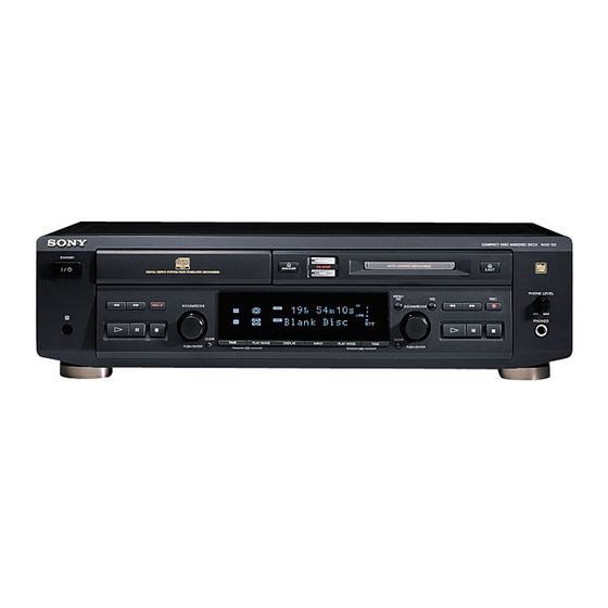
SECTION 2 GENERAL Front view Rear view 4 5 67 8 9 0 1 2 3 1 ?/1 (power) switch 1 LINE (ANALOG) IN jack 2 REC-IT button 2 LINE (ANALOG) OUT jack 3 CD disc tray 3 DIGITAL OPTICAL IN terminal 4 Display window 4 VOLTAGE SELECTOR switch (singapore model only) 5 A OPEN/CLOSE button... -
Page 18: Disassembly
SECTION 3 DISASSEMBLY Note: Follow the disassembly procedure in the numerical order given. LOADING PANEL In removing the front panel with the power not supplied, insert a flat-blade screwdriver into a hole at the bottom of loading section and rotate it counterclockwise. Then, draw out the disc table and remove the loading panel. - Page 19 CD MECHANISM DECK SECTION (CDM14H-5TBD26B) 4 three screws (BVTT3 × 6) 3 lead (with connector) 6 Pulling the front panel in the direction of the arrow A a little, remove the mechanism deck (CDM14H-5TBD26B) in the direction of the arrow B . Note: Don’t pull the front panel in the direction of the arrow A by force.
- Page 20 CD BASE UNIT (BU-5TBD26B) 1 two screws 1 two screws (PTPWHM2.6) (PTPWHM2.6) 2 CD base unit (BU-5TBD26B) 3 two compression springs (932) 3 two compression springs (932) 4 chassis (MD) BD (CD) BOARD 3 two screws (P2 × 3) Note: When routing the lead wires of spindle motor, pass them through a slot in the BD (CD) board, then solder to the motor.
- Page 21 MD MECHANISM DECK SECTION (MDM-5X2B) 5 four step screws (BVTTWH M3) 6 Remove the MD 1 wire (flat type) (27 core) mechanism deck (CN602) (MDM-5X2B) to direction of the arrow. 1 wire (flat type) (23 core) (CN601) 2 connector (CN603) 3 screw (BVTT3 ×...
- Page 22 MD BASE UNIT (MBU-5X2B), BD (MD) BOARD 2 base unit (MBU-5X2B) 5 flexible board (CN104) 6 flexible board (CN101) 1 three screws (P2.6 × 6) 7 BD (MD) board 3 Remove the solder (Seven portion). 4 screw (M1.7 × 4) SW BOARD, LOADING MOTOR (M203) 1 screw (PTPWH M2.6 ×...
- Page 23 MAIN BOARD 2 three connectors (CN603, 901, 902) 3 screw 1 wire (flat type) (29 core) (BVTT3 × 6) 1 wire (flat type) (19 core) (CN501) (CN604) 2 connector (CN451) 2 connector 3 screw (CN502) (BVTT3 × 6) 1 wire (flat type) (27 core) (CN602) 6 MAIN board 4 two screws...
-
Page 24: Test Mode
SECTION 4 TEST MODE MD SECITON Note: MD always plays double speed. 1. PRECAUTIONS FOR USE OF TEST MODE • As loading related operations will be performed regardless of the test mode operations being performed, be sure to check that the disc is stopped before setting and removing it. - Page 25 5. SELECTING THE TEST MODE There are 31 types of test modes as shown below. The groups can be switched by turning the (MD) knob. After selecting [YES] the group to be used, press the button. After setting a certain group, turn the (MD) knob switches between these modes.
- Page 26 5-1. Operating the Continuous Playback Mode 1. Entering the continuous playback mode (1) Set the disc in the unit. (Whichever recordable discs or discs for playback only are available) (2) Turn the (MD) knob and display “CPLAY MODE” (C30). [YES] (3) Press the button to change the display to “CPLAY MID”.
-
Page 27: Functions Of Other Buttons
6. FUNCTIONS OF OTHER BUTTONS Function Contents Sets continuous playback when pressed in the STOP state. When pressed during continuous playback, the tracking servo H (MD) turns ON/OFF. x (MD) Stops continuous playback and continuous recording. M (MD) The sled moves to the outer circumference only when this is pressed. m (MD) The sled moves to the inner circumference only when this is pressed. - Page 28 MEANINGS OF OTHER DISPLAYS Contents Display When Lit When Off During continuous playback (CLV: ON) STOP (CLV: OFF) Tracking servo OFF Tracking servo ON Recording mode ON Recording mode OFF SYNC CLV low speed mode CLV normal mode L.SYNC ABCD adjustment completed OVER Tracking offset cancel ON Tracking offset cancel OFF...
- Page 29 5. ISRC DISPLAY Procedure: (1) Enter the test mode, then rotate (CD) knob to display “4> IRSC”, and press the (CD) knob. (2) Rotating the (CD) knob counterclockwise displays higher-order 5 digits, or clockwise displays lower-order 7 digits. (3) To exit from this mode, press (MD) button and (MD) knob simultaneously.
-
Page 30: Electrical Adjustments
SECTION 5 ELECTRICAL ADJUSTMENTS MD SECTION Note: MD always plays double speed. 1. PARTS REPLACEMENT AND ADJUSTMENT • Check and adjust the mechanism deck as follows. • Abbreviation The procedure changes according to the part replaced : Optical pick-up OWH : Overwrite head •... - Page 31 2. PRECAUTIONS FOR CHECKING LASER DIODE 4. Use the following tools and measuring devices. • Check Disc (MD) TDYS-1 EMISSION (Part No. 4-963-646-01) To check the emission of the laser diode during adjustments, never • Test Disc (MDW-74/AU-1) (Part No. 8-892-341-41) view directly from the top as this may lose your eye-sight.
- Page 32 [YES] 6. CHECK PRIOR TO REPAIRS Note 1: After step 4, each time the button is pressed, the display will be switched “LD 0.7 mW $ ”, “LD 7.5 mW $ ”, and These checks are performed before replacing parts according to “LD Wp ”.
- Page 33 [YES] 6-4. Focus Bias Check 9. Press the button to display “EFB = MO-P”. Then, the optical pick-up moves to the pit area automatically Change the focus bias and check the focus tolerance amount. and servo is imposed. Checking Procedure : 10.
- Page 34 7. INITIAL SETTING OF ADJUSTMENT VALUE 9. TEMPERATURE COMPENSATION OFFSET ADJUSTMENT Note: Save the temperature data at that time in the non-volatile memory Mode which sets the adjustment results recorded in the non-volatile as 25 ˚C reference data. memory to the initial setting value. However the results of the tempera- Note : ture compensation offset adjustment will not change to the initial setting 1.
- Page 35 11. TRAVERSE ADJUSTMENT 6. Turn the (MD) knob so that the reading of [YES] the laser power meter becomes 6.9 to 7.1 mW, press the Note 1: Data will be erased during MO reading if a recorded disc is button to save it. used in this adjustment.
- Page 36 [YES] 8. Turn the (MD) knob so that the waveform 18. Press the button, display “EFB = SAV” for a mo- of the oscilloscope becomes the specified value. ment and save the adjustment results in the non-volatile (When the (MD) knob is turned, the memory.
- Page 37 13. ERROR RATE CHECK 15. AUTO GAIN CONTROL OUTPUT LEVEL ADJUSTMENT 13-1. CD Error Rate Check Be sure to perform this adjustment when the optical pick-up is Checking Procedure : replaced. 1. Load the check disc (MD) TDYS-1. If the adjustment results becomes “Adjust NG!”, the optical pick- 2.
- Page 38 Adjustment Location: – BD (MD) BOARD (Side A) – CN101 D101 CN110 I+3V NOTE IC171 – BD (MD) BOARD (Side B) – IC101 IC121 IC192 Note: It is useful to use the jig for checking the waveform. (Refer to Ser- vicing Notes on page 8)
- Page 39 Note: A clear RF signal waveform means that the shape “◊” can be clearly CD SECTION distinguished at the center of the waveform. Note: RF signal waveform 1. CD Block is basically designed to operate without adjustment. There- VOLT/DIV: 200 mV fore, check each item in order given.
- Page 40 Adjustment Location: – BD (CD) BOARD (SIDE A) – R147 (RFO) (FE) IC101 (TE) IC131 (VC) – MAIN BOARD (SIDE B) – R506 TP (ADJ) R507 R504 IC603 R505 IC604...
-
Page 41: Diagrams
MXD-D3 SECTION 6 DIAGRAMS 6-1. NOTE FOR PRINTED WIRING BOARDS AND SCHEMATIC DIAGRAMS • Circuit Boards Location (In addition to this, the necessary note is printed in each block) Note on Printed Wiring Board: Note on Schematic Diagram: TRANS board •... -
Page 42: Printed Wiring Board - Bd (Cd) Board
MXD-D3 6-2. PRINTED WIRING BOARD – BD (CD) Board – • See page 41 for Circuit Boards Location. (Page • Semiconductor • Semiconductor Location (Side A) Location (Side B) Ref. No. Location Ref. No. Location IC101 IC115 IC171 IC131 IC181... -
Page 43: Schematic Diagram - Bd (Cd) Board
MXD-D3 6-3. SCHEMATIC DIAGRAM – BD (CD) Board – • See page 56 for Waveforms. • See page 57 for IC Block Diagrams. (Page Note on Schematic Diagram: The components identified by mark 0 or dotted Les composants identifiés par une marque 0 sont •... -
Page 44: Schematic Diagram - Bd (Md) Board (1/2)
MXD-D3 6-4. SCHEMATIC DIAGRAM – BD (MD) Board (1/2) – • • See page 56 for Waveforms. See page 59 for IC Block Diagrams. (Page 45) Note on Schematic Diagram: The components identified by mark 0 or dotted Les composants identifiés par une marque 0 sont •... -
Page 45: Schematic Diagram - Bd (Md) Board (2/2)
MXD-D3 6-5. SCHEMATIC DIAGRAM – BD (MD) Board (2/2) – • • See page 56 for Waveforms. See page 60 for IC Block Diagrams. (Page 48) BR24C02F-E2 (Page 44) (Page 49) Note on Schematic Diagram: • Voltages and waveforms are dc with respect to ground under no-signal conditions. -
Page 46: Printed Wiring Board - Bd (Md) Board
MXD-D3 6-6. PRINTED WIRING BOARD – BD (MD) Board – • See page 41 for Circuit Boards Location. (Page 50) (Page 50) • Semiconductor Location (Side B) • Semiconductor Ref. No. Location Location (Side A) IC101 Ref. No. Location IC121... -
Page 47: Schematic Diagram - Main (1/3) /Loading Boards
MXD-D3 6-7. SCHEMATIC DIAGRAM – MAIN (1/3) / LOADING Boards – • See page 56 for Waveform. • See page 62 for IC Block Diagrams. (Page 55) (Page 55) (Page 48) (Page 43) Note on Schematic Diagram: (Page 49) • Voltages and waveforms are dc with respect to ground under no-signal conditions. -
Page 48: Schematic Diagram - Main Board (2/3)
MXD-D3 6-8. SCHEMATIC DIAGRAM – MAIN Board (2/3) – • See page 56 for Waveforms. (Page 53) (Page 45) (Page (Page 55) (Page 49) Note on Schematic Diagram: no mark : MD PLAY 〈〈 〉〉 : CD PLAY • Voltages and waveforms are dc with respect to ground ∗... -
Page 49: Schematic Diagram - Main Board (3/3)
MXD-D3 6-9. SCHEMATIC DIAGRAM – MAIN Board (3/3) – • See page 56 for Waveform. • See page 62 for IC Block Diagrams. (Page 48) (Page 53) (Page (Page 45) Note on Schematic Diagram: • Voltages and waveforms are dc with respect to ground The components identified by mark 0 or dotted Les composants identifiés par une marque 0 sont... -
Page 50: Printed Wiring Board - Main Board (Side A)
MXD-D3 6-10. PRINTED WIRING BOARD – MAIN Board (Side A) – • See page 41 for Circuit Boards Location. • Semiconductor Location (Page 46) (Page 42) (Page 46) (Page 52) Ref. No. Location D401 D943 D966 D967 D968 IC501 IC503... -
Page 51: Printed Wiring Boards - Main (Side B)/Loading Boards
MXD-D3 6-11. PRINTED WIRING BOARDS – MAIN (Side B) / LOADING Boards – • See page 41 for Circuit Boards Location. (Page 54) (Page 54) (Page 55) (Page 52) • Semiconductor Location LOADING BOARD Ref. No. Location Ref. No. Location Ref. -
Page 52: Printed Wiring Boards - Display/Pwsw/Hp Boards
MXD-D3 6-12. PRINTED WIRING BOARDS – DISPLAY / PWSW / HP Boards – • See page 41 for Circuit Boards Location. (Page • Semiconductor Location Ref. No. Location D751 D752 IC751 Q751 Q752 Q753 Q754 (Page 51) -
Page 53: Schematic Diagram - Display/Pwsw/Hp Boards
MXD-D3 6-13. SCHEMATIC DIAGRAM – DISPLAY / PWSW / HP Boards – • See page 56 for Waveform. (Page (Page 49) Note on Schematic Diagram: • Voltages and waveforms are dc with respect to ground under no-signal conditions. no mark : STOP... -
Page 54: Printed Wiring Board - Trans Board
MXD-D3 6-14. PRINTED WIRING BOARD – TRANS Board – • See page 41 for Circuit Boards Location. (Page 51) (Page 51) -
Page 55: Schematic Diagram - Trans Board
Les composants identifiés par une marque 0 sont line with mark 0 are critical for safety. critiques pour la sécurité. Ne les remplacer que Replace only with part number specified. par une pièce portant le numéro spécifié. (Page 48) MXD-D3 SW... - Page 56 MXD-D3 • Waveforms – BD (CD) Board – 1 IC131 qh (RFO) (PLAY MODE) 6 IC101 q; (WFCK) 2 IC601 qg (XIN) 7 IC401 qs (BCLK) qs IC603 8 (2-Q) 5 IC121 wj (LRCK) Approx. 2.6 Vp-p 4.6 Vp-p 4.3 Vp-p 6.8 Vp-p...
- Page 57 • IC Block Diagrams – BD (CD) Board – IC101 CXD2585Q 71 70 62 61 67 66 65 64 63 Digital VPCO DVDD0 Clock V16M Generator XRST VCTL MUTE Interface BIAS Error AVDD1 Corrector DATA XLAT CLOCK FILI Interface Digital Sub Code FILO demodurator...
- Page 58 IC131 CXA2568M-T6 HOLD APC PD AMP LC/PD APC LD AMP – LD ON – – – HOLD SW AGC CONT AGC VTH 50µA RF BOT – – – – RFTC RF SUMMING AMP RF EQ AMP RF I RF O –...
- Page 59 – BD (MD) Board – IC101 CXA2523AR 43 42 USROP – RF AGC – USRC RFA1 BPF3T RFA2 RFA3 PEAK3T – HLPT –1 – – –2 – OFST PTGR TEMP PEAK – –2 – BOTTOM 36 BOTM – –1 GRVA PBSW 35 ABCD 34 FE...
- Page 60 IC121 CXD2656AR 100 99 98 97 96 95 94 93 92 91 90 89 88 87 86 85 84 83 82 81 80 79 78 77 76 SPINDLE GENERATOR SERVO 75 TE MNT0 74 SE MNT1 EACH MONITOR 73 AVSS BLOCK CONTROL MNT2...
- Page 61 IC152 BH6511FS-E2 INTERFACE INTERFACE CHARGE PREDRIVE PREDRIVE PUMP. PREDRIVE PREDRIVE INTERFACE INTERFACE IC171 BR24C02F-E2 TEST INPUT START CYCLE H.V. GENERATION TIMING START & CONTROL STOP LOGIC CONTROL LOGIC E PROM XDEC 32 x 32 LOAD WORD ADDRESS COUNTER YDEC DATA REGISTER...
-
Page 62: Main Board
– MAIN Board – IC401 AK4524-TP IC602 LB1830M-S-TE-L VREF VCONT VCOM VREF AINR AOUTR+ LOGIC PREDRIVER AOUTR– CONVERTER CONVERTER AOUTL+ BLOCK BLOCK AOUTL– AINL VREF AGND DGND TEST XTAO CLOCK XTAI GENERATOR CLKO & DIVIDER XTALE 10 OUT2 OUT1 VS H.P.F. -
Page 63: Ic Pin Function Description
6-18. IC PIN FUNCTION DESCRIPTION • BD (MD) BOARD IC101 CXA2523AR (RF AMP, FOCUS/TRACKING ERROR AMP) Pin No. Pin Name Description I-V converted RF signal I input from the optical pick-up block detector I-V converted RF signal J input from the optical pick-up block detector Middle point voltage (+1.65V) generation output terminal 4 to 9 A to F... - Page 64 • BD (MD) BOARD IC121 CXD2656AR (DIGITAL SIGNAL PROCESSOR, DIGITAL SERVO PROCESSOR, EFM/ACIRC ENCODER/DECODER, SHOCK PROOF MEMORY CONTROLLER, ATRAC ENCODER/DECODER) Pin No. Pin Name Description Focus OK signal output to the system controller (IC601) MNT0 (FOK) “H” is output when focus is on (“L”: NG) MNT1 (SHOCK) Track jump detection signal output to the system controller (IC601) MNT2 (XBUSY)
- Page 65 Pin No. Pin Name Description XCAS Column address strobe signal output to the D-RAM (IC124) “L” active Address signal output to the D-RAM (IC124) XRAS Row address strobe signal output to the D-RAM (IC124) “L” active Write enable signal output to the D-RAM (IC124) “L” active Two-way data bus with the D-RAM (IC124) MVCI I (S)
- Page 66 Pin No. Pin Name Description FRDR Focus servo drive PWM signal (–) output to the BH6511FS (IC152) Clock signal (176.4 kHz) output terminal (X’tal system) Not used (open) SRDR Sled servo drive PWM signal (–) output to the BH6511FS (IC152) SFDR Sled servo drive PWM signal (+) output to the BH6511FS (IC152) SPRD...
- Page 67 • MAIN BOARD IC501 M30625MGA-A50GP (CD MECHANISM CONTROL) Pin No. Pin Name Description Not used (open) LEVEL R R-ch level output to the system controller (IC601) LEVEL L L-ch level output to the system controller (IC601) 4, 5 Not used (open) CNVSS —...
- Page 68 Pin No. Pin Name Description AFADJ Input terminal for the CD test mode setting “L”: AFADJ mode Input terminal for the CD test mode setting “L”: ADJ mode 46, 47 Not used (open) LODOUT Motor drive signal output to the loading motor drive (IC502) “H” active *1 LODIN Motor drive signal output to the loading motor drive (IC502) “H”...
- Page 69 • MAIN BOARD IC601 M30624MG-A10FP (SYSTEM CONTROLLER (MD MECHANISM CONTROLLER)) Pin No. Pin Name Description DACDTI Serial data output to the A/D, D/A converter (IC401) DACCLK Serial data transfer clock signal output to the A/D, D/A converter (IC401) DALATCH Serial data latch pulse signal output to the A/D, D/A converter (IC401) DARESET Reset signal output to the A/D, D/A converter (IC401) “L”: reset XAMUTE...
- Page 70 Pin No. Pin Name Description CDRST Reset signal output to the CD mechanism controller (IC501) 51, 52 Not used (open) Detection input from the loading-out detect switch (S602) PACKOUT “L” at a load-out position, others: “H” LDIN Motor control signal output to the loading motor driver (IC602) “L” active *1 LDOUT Motor control signal output to the loading motor driver (IC602) “L”...
- Page 71 Pin No. Pin Name Description Focus OK signal input from the CXD2656AR (IC121) MNT0 (FOK) “H” is input when focus is on (“L”: NG) Clock signal output to the EEPROM (IC171) MNT2 (XBUSY) Busy signal input from the CXD2656AR (IC121) LINE SEL3 Audio line selection output terminal CSET1...
-
Page 72: Exploded Views
SECTION 7 EXPLODED VIEWS NOTE: • -XX and -X mean standardized parts, so they • Items marked “*” are not stocked since they The components identified by mark 0 or dotted line with mark are seldom required for routine service. Some may have some difference from the original 0 are critical for safety. - Page 73 (2) FRONT PANEL SECTION supplied supplied supplied with RV481 supplied supplied with J481 Ref. No. Part No. Description Remark Ref. No. Part No. Description Remark 4-981-435-01 RING (DIA. 50), ORNAMENTAL (GOLD) 4-220-710-01 PLATE, INDICATION 4-981-435-11 RING (DIA. 50), ORNAMENTAL (BLACK) A-4672-565-A KNOB (AMS) ASSY (BLACK) 4-983-762-02 CUSHION 4-996-687-71 KNOB (AMS) (GOLD)
- Page 74 (3) CHASSIS SECTION US, Canadian AEP, UK, Singapore Chinese Singapore TR102 US, Canadian not supplied not supplied not supplied Singapore not supplied supplied not supplied supplied The components identified by Les composants identifiés par une mark 0 or dotted line with marque 0 sont critiques pour la mark 0 are critical for safety.
- Page 75 (4) MD MECHANISM DECK SECTION (MDM-5X2B) not supplied M203 MBU-5X2B Ref. No. Part No. Description Remark Ref. No. Part No. Description Remark 4-996-227-01 LEVER (HEAD) * 201 1-668-111-11 SW BOARD 4-996-229-01 SPRING (HEAD LEVER), TORSION * 202 4-996-217-01 CHASSIS 4-996-212-01 LEVER (LIMITTER) 4-996-223-01 INSULATOR (F) (BLACK) 4-996-213-01 SPRING (LIMITTER), TORSION * 204...
- Page 76 (5) MD BASE UNIT SECTION (MBU-5X2B) HR901 not supplied not supplied M201 S102 not supplied M202 The components identified by Les composants identifiés par une mark 0 or dotted line with marque 0 sont critiques pour la mark 0 are critical for safety. sécurité.
- Page 77 (6) CD MECHANISM DECK SECTION (CDM14H-5TBD26B) BU-5TBD26B M103 Ref. No. Part No. Description Remark Ref. No. Part No. Description Remark 4-222-283-01 PULLEY (AT) (CDM14) 4-985-672-01 SCREW (+PTPWHM2.6), FLOATING 4-933-110-41 HOLDER (MG) 4-959-996-01 SPRING (932), COMPRESSION 4-213-448-12 TABLE (BL), DISC 4-933-129-01 HOLDER (BU) 4-967-268-01 GEAR (C) 4-933-111-41 CHASSIS (MD) 4-927-649-01 BELT...
- Page 78 (7) CD BASE UNIT SECTION (BU-5TBD26B) M101 M102 The components identified by Les composants identifiés par une mark 0 or dotted line with marque 0 sont critiques pour la mark 0 are critical for safety. sécurité. Replace only with part num- Ne les remplacer que par une pièce ber specified.
-
Page 79: Electrical Parts List
SECTION 8 BD (CD) ELECTRICAL PARTS LIST NOTE: • Due to standardization, replacements in the • Items marked “*” are not stocked since they The components identified by mark 0 or dotted line with mark 0 are seldom required for routine service. parts list may be different from the parts speci- are critical for safety. - Page 80 BD (CD) BD (MD) Ref. No. Part No. Description Remark Ref. No. Part No. Description Remark R113 1-216-097-00 RES, CHIP 100K 1/10W C112 1-163-017-00 CERAMIC CHIP 0.0047uF 5% R114 1-216-025-00 RES, CHIP 1/10W C113 1-109-982-11 CERAMIC CHIP C115 1-164-161-11 CERAMIC CHIP 0.0022uF 10% 100V R116...
- Page 81 BD (MD) Ref. No. Part No. Description Remark Ref. No. Part No. Description Remark < DIODE > R119 1-216-295-00 SHORT R120 1-216-025-00 RES, CHIP 1/10W D101 8-719-988-61 DIODE 1SS355TE-17 R121 1-216-097-00 RES, CHIP 100K 1/10W D181 8-719-046-86 DIODE F1J6TP R123 1-216-295-00 SHORT D183 8-719-046-86 DIODE F1J6TP...
- Page 82 BD (MD) DISPLAY Ref. No. Part No. Description Remark Ref. No. Part No. Description Remark < SWITCH > R704 1-249-429-11 CARBON 1/4W R711 1-249-421-11 CARBON 2.2K 1/4W S101 1-762-596-21 SWITCH, PUSH (1 KEY) (LIMIT) R712 1-247-843-11 CARBON 3.3K 1/4W S102 1-762-148-21 SWITCH, PUSH (2 KEY) R713 1-249-425-11 CARBON...
- Page 83 DISPLAY LOADING MAIN Ref. No. Part No. Description Remark Ref. No. Part No. Description Remark S741 1-762-875-21 SWITCH, KEYBOARD (x (MD)) < CAPACITOR/RESISTOR/SHORT > S742 1-762-875-21 SWITCH, KEYBOARD (X (MD)) S743 1-762-875-21 SWITCH, KEYBOARD (H (MD)) C201 1-136-356-11 FILM 470PF C202 1-128-551-11 ELECT 22uF...
- Page 84 MAIN Ref. No. Part No. Description Remark Ref. No. Part No. Description Remark C512 1-165-319-11 CERAMIC CHIP 0.1uF C922 1-165-319-11 CERAMIC CHIP 0.1uF C513 1-165-319-11 CERAMIC CHIP 0.1uF C923 1-165-319-11 CERAMIC CHIP 0.1uF C514 1-104-665-11 ELECT 100uF C515 1-163-234-11 CERAMIC CHIP 20PF C924 1-104-665-11 ELECT...
-
Page 85: Components Identified By Mark 0 Or Dotted
MAIN Ref. No. Part No. Description Remark Ref. No. Part No. Description Remark <TERMINAL> Q651 8-729-421-22 TRANSISTOR UN2211-TX Q951 8-729-281-53 TRANSISTOR 2SC1815GR-TPE2 EPT901 1-537-770-21 TERMINAL BOARD, GROUND < RESISTOR > < FERRITE BEAD/SHORT > 1-216-295-00 SHORT FB500 1-216-295-00 SHORT 1-216-295-00 SHORT FB501 1-216-295-00 SHORT 1-216-295-00 SHORT... -
Page 86: Components Identified By Mark 0 Or Dotted
MAIN PWSW TRANS Ref. No. Part No. Description Remark Ref. No. Part No. Description Remark R456 1-216-057-00 METAL CHIP 2.2K 1/10W R983 1-216-039-00 METAL CHIP 1/10W R984 1-216-073-00 METAL CHIP 1/10W R501 1-216-065-00 RES, CHIP 4.7K 1/10W R502 1-216-065-00 RES, CHIP 4.7K 1/10W <... -
Page 87: Components Identified By Mark 0 Or Dotted
TRANS Ref. No. Part No. Description Remark Ref. No. Part No. Description Remark < CONNECTOR > 7-621-772-20 SCREW +B 2X5 7-621-772-40 SCREW +B 2X8 * CN103 1-580-230-11 PIN, CONNECTOR (PC BOARD) 2P 7-627-852-08 SCREW, PRECISION +P 1.7X2.5 < RELAY > 7-685-533-19 SCREW, +BTP 2.6X6 TYPE2 N-S 7-685-133-19 SCREW (DIA. - Page 88 MXD-D3 Ref. No. Part No. Description Remark Ref. No. Part No. Description Remark Sony Corporation 9-928-983-11 99I0582-1 Home Audio Company Printed in Japan © 1999. 9 Published by Quality Assurance Dept.