Table of Contents
Advertisement
Quick Links
SERVICE MANUAL
Ver 1.1 2001. 06
MDS-SP55 is the MD section in CMT-SP55MD,
and MDS-SP55 is sold in the option as a
minidisk deck of CMT-SP55TC.
System
MiniDisc digital audio system
Laser
Semiconductor laser (λ=780 nm)
Emission duration: continuous
Laser output
Max. 44.6 µW*
*This output is the value
measured at a distance of 200 mm
from the objective lens surface on
the Optical Pick-up Block with
7 mm aperture.
Sampling frequency
44.1 kHz
Frequency response
20 Hz – 20 kHz
Inputs
DIGITAL OPTICAL CD IN: Optical
DIGITAL OPTICAL AUX IN: Optical
Output
DIGITAL OPTICAL OUT:
Optical
9-929-537-12
Sony Corporation
Home Audio Company
2001F0200-1
Shinagawa Tec Service Manual Production Group
© 2001.6
MDS-SP55
Model Name Using Similar Mechanism
MD Mechanism Type
Optical Pick-up Type
SPECIFICATIONS
General
Dimensions (w/h/d) incl. projecting parts and controls
Mass
Supplied accessories
Design and specifications are subject to change
without notice.
AEP Model
UK Model
E Model
MDS-JE330
MDM-5A
KMS-260B/S1NP
Approx. 202 × 101 × 298 mm
Approx. 1.7 kg
System cable (1)
Digital cable (1)
MINIDISC DECK
1
Advertisement
Chapters
Table of Contents

Related Manuals for Sony MDS-SP55


Summary of Contents for Sony MDS-SP55
- Page 1 AEP Model UK Model E Model Ver 1.1 2001. 06 MDS-SP55 is the MD section in CMT-SP55MD, and MDS-SP55 is sold in the option as a minidisk deck of CMT-SP55TC. Model Name Using Similar Mechanism MDS-JE330 MD Mechanism Type MDM-5A...
- Page 2 DIGITAL following list. If any problem persists, consult OPTICAL IN jack properly using a digital C13/Read Error your nearest Sony dealer. connecting cable (an optical cable) (not The MD deck cannot read the disc information supplied (See page 39).
- Page 3 ITEMS OF ERROR HISTORY MODE ITEMS AND CONTENTS Selecting the Test Mode Display Details of History Displays the recording time. total rec Displayed as “rssssssh”. The displayed time is the total time the laser is set to the high power state. This is about 1/4 of the actual recording time.
- Page 4 COMPONENTS IDENTIFIED BY MARK 0 OR DOTTED LINE WITH MARK 0 ON THE SCHEMATIC DIAGRAMS AND IN THE PARTS LIST ARE CRITICAL TO SAFE OPERATION. REPLACE THESE COMPONENTS WITH SONY PARTS WHOSE PART NUMBERS APPEAR AS SHOWN IN THIS MANUAL OR IN SUPPLEMENTS PUBLISHED BY SONY.
-
Page 5: Table Of Contents
TABLE OF CONTENTS 1. SERVICING NOTE ............6 2. GENERAL ................ 13 3. DISASSEMBLY 3-1. Case ..................14 3-2. Front Panel Assy ..............14 3-3. MD Mechanism Deck (MDM-5A) ........15 3-4. Main Board ................. 15 3-5. Slider (Cam) ................ 16 3-6. -
Page 6: Servicing Note
SECTION 1 SERVICING NOTE This unit cannot be repaired by itself. When repairing, connect the whole system except for the speaker. CD Text Display • This unit displays CD text. Text is displayed for the first 50 track only and will not be displayed from the 51st track onwards. Do not suspect a fault in this case. In some cases, some special characters will not be displayed and may be replaced by other characters. - Page 7 JIG FOR CHECKING BD BOARD WAVEFORM The special jig (J-2501-149-A) is useful for checking the waveform of the BD board. The names of terminals and the checking items to be performed are shown as follows. GND : Ground I+3V : For measuring IOP (Check the deterioration of the optical pick-up laser) IOP : For measuring IOP (Check the deterioration of the optical pick-up laser) TEO : TRK error signal (Traverse adjustment) : Reference level for checking the signal...
- Page 8 IOP DATA RECORDING AND DISPLAY WHEN OPTICAL PICK-UP AND NON-VOLATILE MEMORY (IC171 OF BD BOARD) ARE REPLACED The IOP value labeled on the optical pick-up can be recorded in the non-volatile memory. By recording the value, it will eliminate the need to look at the value on the label of the optical pick-up.
- Page 9 CHECKS PRIOR TO PARTS REPLACEMENT AND ADJUSTMENTS Before performing repairs, perform the following checks to determine the faulty locations up to a certain extent. Details of the procedures are described in “5 Electrical Adjustments”. Criteria for Determination Measure if unsatisfactory: (Unsatisfactory if specified value is not satisfied) Laser power check •...
- Page 10 RETRY CAUSE DISPLAY MODE • In this test mode, the causes for retry of the unit during recording can be displayed on the fluorescent indicator tube. During playback, the “track mode” for obtaining track information will be set. This is useful for locating the faulty part of the unit. •...
- Page 11 Reading the Track Mode Display Higher Bits Lower Bits Details Hexa- Hexadecimal decimal b7 b6 b5 b4 b3 b2 b1 b0 When 0 When 1 Binary Emphasis ON Emphasis OFF Monaural Stereo This is 2-bit display. Normally 01. 01:Normal audio. Others:Invalid Audio (Normal) Invalid Digital copy...
- Page 12 SERVICING POSITION 1. Remove the four screws securing the upper case, and remove the upper case. 2. Remove the three screws A securing the rear panel. 3. Remove the two craws B securing the MAIN board. 4. Remove the MAIN board with the rear panel.
-
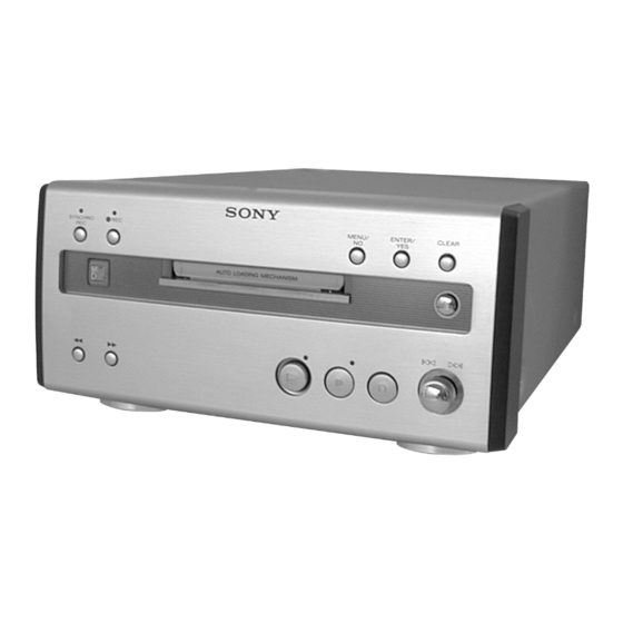
Page 13: General
SECTION 2 GENERAL CD SYNC REC button l L knob CD SYNC REC indicator s button z REC button S indicator z REC indicator S button H insdicator MENU/NO button H button ENTER/YES button CLEAR button M button A button m button... -
Page 14: Disassembly
SECTION 3 DISASSEMBLY Case Front Panel Assy Main Board (Page 15) MD Mechanism Deck (MDM-5A) (Page 15) Slider (Cam) BD Board Spindle Motor, Sled Motor (Page 16) (page 16) (page 17) Optical pick-up Over Write Head (Page17) (page 17) Note: Follow the disassembly procedure in the numerical order given. 3-1. -
Page 15: Md Mechanism Deck (Mdm-5A)
3-3. MD MECHANISM DECK (MDM-5A) 4 two screws 4 two screws (BVTPWH M3) (BVTPWH M3) 5 MD mechanism deck 1 flat type wire (23 core) (CN702) 2 flat type wire (21 core) (CN501) 3 connector (CN701) 3-4. MAIN BOARD 3 panel back 5 main board 1 six screws (BVTP 3x8) -
Page 16: Slider (Cam)
3-5. SLIDER (CAM) 6 slider (cam) • Note for installation of Slider (CAM) Set the shaft of Cam gear to be at the position in the figure. 2 bracket (guide L) 1 two screws (BTP 2.6x6) Set the shaft of Lever (O/C) to 3 leaf spring be at the position in the figure. -
Page 17: Over Write Head
3-7. OVER WRITE HEAD 3-8. OPTICAL PICK-UP (KMS-260B/S1NP) Note: 2 screw (P 1.7x6) Turn the optical pick-up 5 optical pick-up (for MD) inside out, and pull out the flexible board. 3 over write head (HR901) 4 flexible board 1 flexible board 1 screw (B 2x8) 2 leaf spring (SHAFT) -
Page 18: Test Mode
SECTION 4 TEST MODE 4-1. PRECAUTIONS FOR USE OF TEST MODE • As loading related operations will be performed regardless of the test mode operations being performed, be sure to check that the disc is stopped before setting and removing it. Even if the A button (MD) is pressed while the disc is rotating during continuous playback, continuous recording, etc., the disc will not stop rotating. - Page 19 4-5. SELECTING THE TEST MODE There are 31 types of test modes as shown below. The groups can be switched by rotating the l L knob (MD). After selecting the group to be used, press the ENTER/YES button (MD). After setting a certain group, rotating the l L knob (MD) switches between these modes.
- Page 20 4-5-1. Operating the Continuous Playback Mode 1. Entering the continuous playback mode 1 Set the disc in the unit. (Whichever recordable discs or discs for playback only are available.) 2 Rotate the l L knob (MD) and display “MD CPLAY MODE”. 3 Press the ENTER/YES button (MD) to change the display to “MD CPLAY MID”.
-
Page 21: Functions Of Other Buttons
4-6. FUNCTIONS OF OTHER BUTTONS Function Contents Sets continuous playback state. playback, the tracking servo turns ON. Stops continuous playback and continuous recording. The sled moves to the outer circumference only when this is pressed. The sled moves to the inner circumference only when this is pressed. zREC ON/OFF of recording head arm each time the button is pressed. -
Page 22: Electrical Adjustments
SECTION 5 ELECTRICAL ADJUSTMENTS 5-1. PARTS REPLACEMENT AND ADJUSTMENT • Check and adjust the MDM and MBU as follows. The procedure changes according to the part replaced • Abbreviation : Optical pick-up OWH: Overwrite head • Temperature compensation offset check (5-6-1) •... - Page 23 5-2. PRECAUTIONS FOR CHECKING LASER DIODE 4) Use the following tools and measuring devices. • Check Disc (MD) TDYS-1 EMISSINON (Parts No. 4-963-646-01) To check the emission of the laser diode during adjustments, never • Test Disk (MDW-74/AGA-1) (Parts No. 4-229-747-01) view directly from the top as this may lose your eye-sight.
-
Page 24: Traverse Check
5-6. CHECKS PRIOR TO REPAIRS Note 1: After step 4, each time the ENTER/YES button is pressed, the display will be switched between “MD LD 0.7 mW $ These checks are performed before replacing parts according to ”, “MD LD 0.7 mW $ ”, “MD LD 6.2 mW $ ”, “approximate specifications”... -
Page 25: C Play Check
10. Observe the waveform of the oscilloscope, and check that the 5-6-4. Focus Bias Check specified value is satisfied. Do not rotate the m button or Change the focus bias and check the focus tolerance amount. M button. Checking Procedure : 1. -
Page 26: Initial Setting Of The Adjustment Value
5-7. INITIAL SETTING OF ADJUSTMENT VALUE 5-9. TEMPERATURE COMPENSATION OFFSET ADJUTMENT Note: Save the temperature data at that time in the non-volatile memory Mode which sets the adjustment results recorded in the non-volatile as 25 ˚C reference data. memory to the initial setting value. However the results of the Note : temperature compensation offset adjustment will not change to the 1. -
Page 27: Traverse Adjustment
5. Then “MD LD 7.0 mW $ ” will be displayed. 5-11. TRAVERSE ADJUSTMENT 6. Rotate the l L knob so that the reading of the laser Connection : power meter becomes 6.9 to 7.1 mW, press the ENTER/YES Oscilloscope button and save it. -
Page 28: Focus Bias Adjustment
9. Press the ENTER/YES button, and save the adjustment results 5-12. FOCUS BIAS ADJUSTMENT in the non-volatile memory. (“MD EFB = SAVE” will be Adjusting Procedure : displayed for a moment.) 1. Load a test disk (MDW-74/GA-1). 10. “MD EFB = MO-P”. -
Page 29: Error Rate Check
5-13. ERROR RATE CHECK 5-15. AUTO GAIN CONTROL OUTPUT LEVEL 5-13-1. CD Error Rate Check ADJUSTMENT Checking Procedure : Be sure to perform this adjustment when the pick-up is replaced. 1. Load a check disc (MD) TDYS-1. If the adjustment results becomes “Adjust NG!”, the pick-up may 2. - Page 30 5-16. ADJUSTING POINTS AND CONNECTING POINTS [BD BOARD] (SIDE A) CN101 D101 CN110 I+3V NOTE IC171 [BD BOARD] (SIDE B) IC101 IC121 IC192 NOTE: It is useful to use the jig. for checking the waveform. (Refer to Servicing Note on page 7.)
-
Page 31: Diagrams
SECTION 6 DIAGRAMS WAVEFORMS THIS NOTE IS COMMON FOR PRINTED WIRING • Indication of transistor – BD (1/2) SECTION – – MAIN SECTION – BOARDS AND SCHEMATIC DIAGRAMS. (In addition to this, the necessary note is printed IC701 qd (XOUT) IC101 ek RF PLAY MODE in each block.) These are omitted... -
Page 32: Block Diagrams
MDS-SP55 6-1. BLOCK DIAGRAMS DIGITAL SERVO SIGNAL PROCESSOR, DIGITAL SIGNAL PROCESSOR EFM/ACIRC ENCODER/DECODER, SHOCK-PROOF MEMORY CONTROLLER, – BD SECTION – ATRAC ENCODER/DECODER IC121 OVER WRITE HEAD DRIVE IC181 HR901 OVER WRITE • DIN0 HEAD D-IN.0 • R-ch is omitted. •... -
Page 33: Main Section
MDS-SP55 – MAIN SECTION – IC601(1/4) IC501 X601 IC503 22.579MHz IN 1 512FS IN 2 IC502 IC601(2/4) IC601(3/4,4/4) CLOCK OSC 1D-IN. IC201 D-IN.0 CN707 A/D,D/A CONVERTER D-OUT VINL1 REC-L 512FS VINL2 DATAO ADDT VINR1 REC-R VINR2 VOUTL MD-L DATAI DADT... -
Page 34: Printed Wiring Board - Bd Section
MDS-SP55 6-2. PRINTED WIRING BOARD – BD SECTION – (Page 39) (Page 39) • Semiconductor • Semiconductor Location Location Ref. No. Location Ref. No. Location D101 D181 IC101 D183 IC121 IC124 IC103 IC152 IC123 IC181 IC171 IC192 Q102 Q101 Q103... -
Page 35: Schematic Diagram - Bd (1/2) Section
MDS-SP55 6-3. SCHEMATIC DIAGRAM – BD (1/2) SECTION – • See page 31 for Waveforms. • See page 42 for IC Block Diagrams. • See page 45 for IC Pin Functions. R130 PIN FUNCTION Note: The components identified by mark 0... -
Page 36: Schematic Diagram - Bd (2/2) Section
MDS-SP55 6-4. SCHEMATIC DIAGRAM – BD (2/2) SECTION – (Page 35) (Page 35) (Page 35) (Page 35) (Page 35) (Page 35) (Page 35) R198 0 (Page 37) PIN FUNCTION (Page 37) BA033FP-E2... -
Page 37: Schematic Diagram - Main (1/2) Section
MDS-SP55 6-5. SCHEMATIC DIAGRAM – MAIN (1/2) SECTION – (Page 42) PIN FUNCTION (Page 36) (Page 38) (Page 36) -
Page 38: Schematic Diagram - Main (2/2) Section
MDS-SP55 6-6. SCHEMATIC DIAGRAM – MAIN (2/2) SECTION – (Page 37) (Page 41) -
Page 39: Printed Wiring Board - Main Section
MDS-SP55 6-7. PRINTED WIRING BOARD – MAIN SECTION – • Semiconductor Location Ref. No. Location D811 D812 D813 D814 D821 D823 D824 IC201 IC301 IC501 IC502 IC503 IC601 IC701 IC821 IC822 IC831 Q301 Q302 There are a few cases that the part isn’t mounted in model is printed on diagram. -
Page 40: Printed Wiring Board - Panel Section
MDS-SP55 6-8. PRINTED WIRING BOARD – PANEL SECTION – (Page 39) • Semiconductor Location Ref. No. Location D921 D922 D923 D924 Q921 Q922 Q923 There are a few cases that the part isn’t mounted in Q924 model is printed on diagram. -
Page 41: Schematic Diagram - Panel Section
MDS-SP55 6-9. SCHEMATIC DIAGRAM – PANEL SECTION – (Page 38) -
Page 42: Schematic Diagram - Bd Switch Section
MDS-SP55 6-10. SCHEMATIC DIAGRAM – BD SWITCH SECTION – 6-12. IC BLOCK DIAGRAMS – BD Section – IC101 CXA2523AR 43 42 USROP – RF AGC (Page 37) – USRC RFA1 BPF3T RFA2 PEAK3T – HLPT –1 – – –2 –... - Page 43 IC121 CXD2654R 100 99 98 97 96 95 94 93 92 91 90 89 88 87 86 85 84 83 82 81 80 79 78 77 76 SPINDLE GENERATOR SERVO 75 TE MNT0 74 SE MNT1 MONITOR EACH 73 AVSS CONTROL BLOCK MNT2...
- Page 44 • MAIN section IC201 UDA1341TS VINL2 VINR2 0DB/6DB 0DB/6DB ADC2R ADC2L VINL1 VINR1 SWITCH SWITCH ADC1L ADC1R AGCSTAT VDDD DIGITAL AGC VSSD DIGITAL MIXER DECIMATION FILTER OVERFLOW DATAO L3CLOCK DIGITAL L3-BUS L3MODE INTERFACE INTERFACE L3DATA DATAI DSP FEATURES SYSCLK PRAK INTERPOLATION FILTER QMUTE DETECTOR...
-
Page 45: Ic Pin Functions
6-13. IC PIN FUNCTIONS • IC101 RF Amplifier (CXA2523AR) (BD board) Pin No. Pin Name Function I-V converted RF signal I input I-V converted RF signal J input Middle point voltage (+1.5V) generation output 4 to 9 A to F Signal input from the optical pick-up detector Light amount monitor input Laser APC output... - Page 46 • IC121 Digital Signal Processor, Digital Servo Signal Processor, EFM/ACIRC Encoder/Decoder, Shock-proof Memory Controller, ATRAC Encoder/Decoder, 2M Bit DRAM (CXD2654R) (BD board) Pin No. Pin Name Function FOK signal output to the system control (monitor output) MNT0 (FOK) “H” is output when focus is on MNT1 (SHCK) Track jump detection signal output to the system control (monitor output) MNT2 (XBUSY)
- Page 47 Pin No. Pin Name Function MVCI I (S) Clock input from an external VCO (Fixed at “L”) ASYO Playback EFM duplex signal output ASYI I (A) Playback EFM comparator slice level input AVDD +3V power supply (Analog) — BIAS I (A) Playback EFM comparator bias current input I (A) Playback EFM RF signal input...
- Page 48 • IC701 M30624MGA-A53FP MASTER CONTROL (MAIN BOARD) Pin No. Pin Name Function MD WM LINK data out (Not used) WMOUT MD WM LINK clock in (Fixed at “L”) WMCLK LEVEL-L DA output (Not used) LEVEL-L LEVEL-R DA output (Not used) LEVEL-R LED DRIVER DATA output (Not used) LEDDATA...
- Page 49 Pin No. Pin Name Function CHAK-IN Detection signal from chucking-in switch HOME Detection signal from HOME switch (Fixed at “L”) PACK-OUT Detection signal from loading out (Loading out position: “L”, others: “H”) switch LDIN Loading motor in control LDOUT Loading motor out control LD-LOW Loading motor voltage control output (Low voltage: “H”) LDON...
-
Page 50: Exploded Views
SECTION 7 EXPLODED VIEWS NOTE: • -XX and -X mean standardized parts, so they • Items marked “*” are not stocked since they The components identified by mark 0 or dotted line with mark are seldom required for routine service. Some may have some difference from the original 0 are critical for safety. -
Page 51: Mechanism Deck Section (Mdm-5A)
7-2. MECHANISM DECK SECTION (MDM-5A) not supplied M903 MBU-5A Ref. No. Part No. Description Remark Ref. No. Part No. Description Remark * 301 1-671-115-21 SW BOARD 4-996-224-01 SCREW (1.7X3), +PWH * 302 4-996-217-01 CHASSIS 4-996-227-14 LEVER (HEAD) 4-996-223-11 INSULATOR (F) * 304 4-996-218-01 BRACKET (GUIDE R) 4-996-229-01 SPRING (HEAD LEVER), TORSION... -
Page 52: Base Unit Section (Mbu-5A)
7-3. BASE UNIT SECTION (MBU-5A) HR901 not supplied not supplied M901 S102 M902 Ref. No. Part No. Description Remark Ref. No. Part No. Description Remark A-469-989-3A BD BOARD, COMPLETE 4-996-261-01 GEAR (SL-B) 3-372-761-01 SCREW (M1.7), TAPPING 4-211-036-01 SCREW (1.7X2.5), +PWH * 353 4-996-267-01 BASE (BU-D) 4-996-265-01 SHAFT, MAIN... -
Page 53: Electrical Parts List
SECTION 8 ELECTRICAL PARTS LIST NOTE: • Due to standardization, replacements in the • Items marked “*” are not stocked since they The components identified by mark 0 or dotted line with mark parts list may be different from the parts speci- are seldom required for routine service. - Page 54 MAIN Ref. No. Part No. Description Remark Ref. No. Part No. Description Remark < COIL > R144 1-216-025-11 RES-CHIP 1/10W R145 1-216-073-00 METAL CHIP 1/10W L101 1-414-813-11 FERRITE R146 1-216-037-00 METAL CHIP 1/10W L102 1-414-813-11 FERRITE R147 1-216-025-11 RES-CHIP 1/10W L103 1-414-813-11 FERRITE R148...
- Page 55 Ver 1.1 2001.06 MAIN Ref. No. Part No. Description Remark Ref. No. Part No. Description Remark C204 1-163-038-11 CERAMIC CHIP 0.1uF D813 8-719-200-82 DIODE 11ES2-TB5 C205 1-128-832-11 ELECT 220uF D814 8-719-200-82 DIODE 11ES2-TB5 C206 1-128-832-11 ELECT 220uF D821 8-719-988-61 DIODE 1SS355TE-17 C207 1-128-832-11 ELECT 220uF...
- Page 56 MAIN PANEL Ref. No. Part No. Description Remark Ref. No. Part No. Description Remark R452 1-216-097-11 RES-CHIP 100K 1/10W < CONNECTOR > R453 1-216-025-11 RES-CHIP 1/10W R501 1-216-057-00 METAL CHIP 2.2K 1/10W CN921 1-784-733-11 CONNECTOR, FFC 11P R502 1-216-089-11 RES-CHIP 1/10W R503 1-216-057-00 METAL CHIP...
- Page 57 Ref. No. Part No. Description Remark Ref. No. Part No. Description Remark MISCELLANEOUS *************** 1-590-218-11 WIRE (FLAT TYPE) (11 CORE) 1-783-140-11 WIRE (FLAT TYPE) (23 CORE) 1-783-139-11 WIRE (FLAT TYPE) (21 CORE) 1-569-972-21 SOCKET, SHORT 2P * 358 1-667-954-11 FLEXIBLE BOARD 0 360 A-4672-541-A OPTICAL PICK-UP KMS-260B/S1NP HR901...
- Page 58 MDS-SP55 REVISION HISTORY Clicking the version allows you to jump to the revised page. Also, clicking the version at the upper right on the revised page allows you to jump to the next revised page. Ver. Date Description of Revision 2001.06...