Philips LX3950W/01 Service Manual
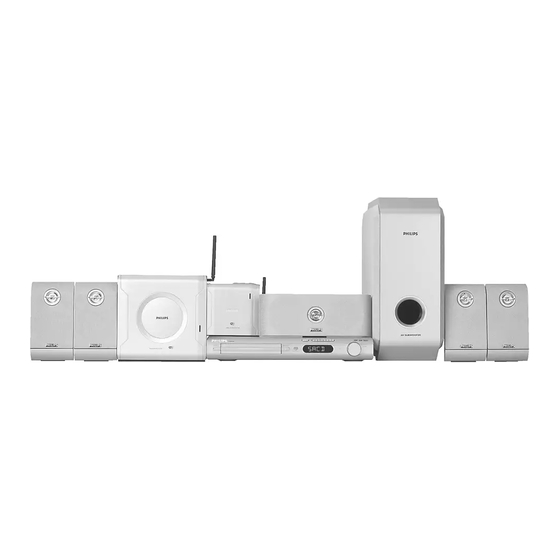
Dvd receiver
Hide thumbs
Also See for LX3950W/01:
- Technical specifications (2 pages) ,
- Quick start manual (49 pages)
Table of Contents
Advertisement
Quick Links
DVD Receiver
Service
Service
Service
Service
Service
Service Manual
©
Copyright 2004 Philips Consumer Electronics B.V. Eindhoven, The Netherlands
All rights reserved. No part of this publication may be reproduced, stored in a retrieval system or
transmitted, in any form or by any means, electronic, mechanical, photocopying, or otherwise
without the prior permission of Philips.
Published by BB 0411 Service Audio
Version 1.0
TABLE OF CONTENTS
Location of pc boards & Version variations ................ 1-2
Technical Specifications ............................................. 1-3
Measurement setup .................................................... 1-4
Service Aids, Safety Instruction, etc. ......................... 1-5
Disassembly Instructions & Service positions .............. 2
Service Test Program ................................................. 3-1
Region code, Software version & upgrades ............... 3-2
Set Block diagram ...................................................... 4-1
Set Wiring diagram ..................................................... 5-1
Front Board .................................................................... 6
AV Board ........................................................................ 7
Amplifier Board .............................................................. 8
Speaker Connector Board ............................................. 9
Module SD6.1 RX ........................................................ 10
Wireless Speaker System ........................................... 11
Set Mechanical Exploded view & parts list ................. 12
Printed in The Netherlands
Subject to modification
LX3950W/
Page
CLASS 1
LASER PRODUCT
GB
01
3139 785 30580
Advertisement
Chapters
Table of Contents

Related Manuals for Philips LX3950W/01


Summary of Contents for Philips LX3950W/01
- Page 1 LASER PRODUCT © Copyright 2004 Philips Consumer Electronics B.V. Eindhoven, The Netherlands All rights reserved. No part of this publication may be reproduced, stored in a retrieval system or transmitted, in any form or by any means, electronic, mechanical, photocopying, or otherwise without the prior permission of Philips.
-
Page 2: Location Of Pc Boards
LOCATION OF PC BOARDS Tuner Module SD6.1 RX Board AV Board DVD Loader Speaker Connector Board Amplifier Board Front Board PSU Board VERSION VARIATIONS: Type /Versions: LX3950W Features & Board in used: Progressive Scan Voltage Selector Digital In TV-In Aux-In Line-Out CVBS Output S-Video Output... - Page 3 SPECIFICATIONS Input sensitivity GENERAL: Aux In : 1V ± 3dB at 39kΩ Mains voltage : 120V for /17 Scart In : 500mV ± 3dB at 39kΩ 220-240V for /01/05/75 Output sensitivity 110-127V/220-240V Switchable for /69 Line Out (Left/Right) : 0.7V ± 2dB at 47kΩ Mains frequency : 50/60Hz Scart Out (Left/Right) : 0.6V ±...
- Page 4 MEASUREMENT SETUP Tuner FM Bandpass LF Voltmeter 250Hz-15kHz e.g. PM2534 e.g. 7122 707 48001 RF Generator e.g. PM5326 S/N and distortion meter e.g. Sound Technology ST1700B Use a bandpass filter to eliminate hum (50Hz, 100Hz) and disturbance from the pilottone (19kHz, 38kHz). Tuner AM (MW,LW) Bandpass LF Voltmeter...
- Page 5 SERVICE AIDS Service Tools: Universal Torx driver holder ........4822 395 91019 Torx bit T10 150mm ..........4822 395 50456 Torx driver set T6 - T20 ......... 4822 395 50145 Torx driver T10 extended ........4822 395 50423 Compact Disc: SBC426/426A Test disc 5 + 5A ......
- Page 6 WAARSCHUWING WARNING Alle IC’s en vele andere halfgeleiders zijn All ICs and many other semi-conductors are gevoelig voor electrostatische ontladingen (ESD). susceptible to electrostatic discharges (ESD). Onzorgvuldig behandelen tijdens reparatie kan Careless handling during repair can reduce life de levensduur drastisch doen verminderen. drastically.
- Page 7 DISMANTLING INSTRUCTIONS Dismantling of the DVD Loader 1) The tray can be manually open by inserting a minus 4) Loosen 4 screws D (see Figure 5) to remove the DVD screw driver and push the lever in the direction as shown Loader (pos 1103-0001).
- Page 8 SERVICE POSITIONS SD6.1 RX Board AV Board Thick Insulation Sheet Thick Insulation Sheet Amplifier Board Speaker Connector Board...
- Page 9 SERVICE TEST PROGRAM To start service test program hold S button depressed while set is in standby * Mains power to set must be on and press H old S button depressed till the Display shown "SVxx-yy" the STANDBY button* S refers to Service Mode V refers to Version Display shows the...
- Page 10 <9> <9> <9> <9> <AUDIO> <3> ..for LX3900SA/69 Trade mode. <9> <9> <9> <9> <AUDIO> <4> ..for LX3900SA/75 <9> <9> <9> <9> <AUDIO> <5> ... for LX3950W/01 To activate Trade Mode: <9> <9> <9> <9> <AUDIO> <6> ... for LX3950W/05 1) Power up the set and select DISC source.
- Page 11 SET BLOCK DIAGRAM HEADPHONE 650mV 78dBA 3.2dB 2.5V 78dBA 3.2dB 74HC4052 TDA8920 TUNER RDS IC POWER AMP (TM 08) SAA6581T TDA8920 SURROUND POWER AMP 1/2xTDA8920 1/2XTDA8920 M62320FP CHIP SELECT I 2 C BUS SHIFT TRANSCEIVER DATA LATCHES I/O PORT 32.767 kHz 4MHz Block Diagram_3139 119 37581_dd wk0402...
- Page 12 SET WIRING DIAGRAM ( Display Board ) NC / Line 2 NC / Line 2 ( PSU Board ) SCART1/Line3 SCART1/Line3 SCART0/Line3 SCART0/Line3 AV_MUTE AV_MUTE Y_REF Y_REF C_REF C_REF CVBS_REF CVBS_REF CVBS CVBS SD6.1 RX Board G_REF G_REF B_REF B_REF R_REF R_REF PCMLRCLK...
- Page 13 FTD DISPLAY PIN CONNECTION FRONT BOARD TABLE OF CONTENTS ( 1G - 8G ) FTD Display Pin Connection ........... 6-1 Display part - Top & Bottom View Layout ......6-2 Display part - Circuit Diagram ......... 6-3 Key part - Layout & Circuit diagram ........ 6-4 Standby part - Layout &...
- Page 14 DISPLAY BOARD - TOP VIEW LAYOUT This assembly drawing shows a summary of all possible versions. For components used in a specific version see schematic diagram and respective parts list. 3139 113 3531 pt4 dd wk0403 DISPLAY BOARD - BOTTOM VIEW LAYOUT This assembly drawing shows a summary of all possible versions.
- Page 15 DISPLAY BOARD - CIRCUIT DIAGRAM 1700 A1 6712 E11 1701 A4 6713 F12 1702 A11 6714 F12 1703 D12 6715 F12 DISPLAY BOARD 1704 D12 6716 F12 1706 C3 6717 F12 1711 D1 6718 F13 1712 E2 6719 F13 +5VDSTBY 1713 F3 7700 A5 FE-BT-VK-N...
- Page 16 KEY BOARD - COMPONENT LAYOUT KEY BOARD - CHIP LAYOUT This assembly drawing shows a summary of all possible versions. This assembly drawing shows a summary of all possible versions. 3139 113 3531 pt4 dd wk0403 For components used in a specific version see schematic diagram and respective parts list. 3139 113 3531 pt4 dd wk0403 For components used in a specific version see schematic diagram and respective parts list.
- Page 17 STANDBY BOARD - COMPONENT LAYOUT STANDBY BOARD - CHIP LAYOUT ELECTRICAL PARTS LIST - FRONT BOARD MISCELLANEOUS 1700 4822 267 10733 Flex Connector 4P 3707 4822 051 30339 33R 5% 0,062W 1701 2422 540 98518 RES CER 8MHz 3708 4822 051 30339 33R 5% 0,062W 1702 3139 111 04131...
- Page 18 ELECTRICAL PARTS LIST - FRONT BOARD DIODES 6700 4822 130 30621 1N4148 6701 3198 020 55680 DIO REG SM PDZ5.6B 6702 9340 548 54115 DIO REG SM PDZ6.2B 6703 4822 130 30621 1N4148 6704 4822 130 30621 1N4148 6705 4822 130 34173 BZX79-C5V6 6706 4822 130 34173...
-
Page 19: Table Of Contents
BRIEF INTRODUCTION OF THE AV BOARD The AV Board consists of the following features : a. IC CS42418 IC CS42418 which includes functions such as ADC and DAC, sound control, volume control and muting function. Sound features such as DSC are controllable via I C Bus from the SD6.1 module. -
Page 20: Top View Layout
AV BOARD - TOP VIEW LAYOUT This assembly drawing shows a summary of all possible versions. For components used in a specific version see schematic diagram and respective parts list. 3139 113 3532 pt5 dd wk0403... - Page 21 AV BOARD - TOP VIEW LAYOUT (MAPPING) AV BOARD - BOTTOM VIEW LAYOUT (MAPPING)
-
Page 22: Bottom View Layout
AV BOARD - BOTTOM VIEW LAYOUT This assembly drawing shows a summary of all possible versions. For components used in a specific version see schematic diagram and respective parts list. 3139 113 3532 pt5 dd wk0403... - Page 23 AV BOARD - CIRCUIT DIAGRAM (PART 1) 1100 A2 7100 B3 1101 C2 7102 C7 1102 E2 7104-A G9 1103 H3 7104-B H9 1100 FE-BT-VK-N 2100 C3 7105 I4 2101 C3 7107 H5 Tu_CLK 2102 C7 7108 I4 TU_DO_STEREO 2103 C5 2105 C5 TU_Dat_In 2108 D5...
-
Page 24: Circuit Diagram (Part 2)
AV BOARD - CIRCUIT DIAGRAM (PART 2) 1200 C1 3247 E13 2200 A6 3248 E10 2201 A13 3250 E12 2202 A8 3251 E3 3200 2203 A6 3252 E11 PCM_Data_Mic_In 2200 2204 A11 3253 E12 PCMCLK 2205 A12 3254 F10 100n 3201 2206 A13 3256 F12... - Page 25 AV BOARD - CIRCUIT DIAGRAM (PART 3) 1300 A12 7306 B7 1301 D12 7307 B9 1302 F2 7308 A3 1303 G3 7309 C9 1300 FE-BT-VK-N 2300 A6 7310 D7 2300 3300 3301 3302 2301 A9 7311 D9 2302 A9 7312 E7 680R 680R 100R...
- Page 26 AV BOARD - CIRCUIT DIAGRAM (PART 4) 1400 A12 1405-A E13 1411 G2 2403 A11 2407 B8 2411 B8 2415 E7 2419 D13 2424 H11 2428 E8 2441 F11 2446 H6 3404 A12 3408 B12 3413 B8 3418 C10 3424 D10 3428 C5 3434 E4 3438 G11...
- Page 27 AV BOARD - CIRCUIT DIAGRAM (PART 5) 1500 A1 1502 D1 2501 D8 2503 D2 2505 E6 2507 E2 2509 E3 2511 E3 3503 B5 3505 C2 3507 C3 3509 D7 3511 E7 3513 E7 4500 A3 5501 C6 6500 C3 7501 C4 7503 C3 7505 D7...
- Page 28 7-10 7-10 AV BOARD - CIRCUIT DIAGRAM (PART 6) 1600 B9 2601 A1 2603 B5 2606 D1 3600 A1 3604 B4 3605 B5 3606 B6 3608 B6 3610 B5 3611 B6 3613 C4 3614 C6 3617 C1 7601 B4 7602 B5 7603 B5 7604 B6 7605 C4...
- Page 29 7-11 7-11 ELECTRICAL PARTS LIST - AV BOARD ELECTRICAL PARTS LIST - AV BOARD MISCELLANEOUS 1100 4822 267 11039 Flex Connector 11P 2148 4822 126 14241 330pF 50V 2257 4822 126 14249 560pF 10% 50V 2411 3198 016 31020 1nF 25V 1103 2422 026 05462 Soc Cinch 4P (Aux-in/Line-out)
-
Page 30: Electrical Parts List
7-12 7-12 ELECTRICAL PARTS LIST - AV BOARD ELECTRICAL PARTS LIST - AV BOARD RESISTORS 3123 4822 051 30681 680R 5% 0,062W 3212 4822 051 30562 5k6 5% 0,063W 3268 4822 051 30183 18k 5% 0,062W 3334 4822 051 30681 680R 5% 0,062W 3124 4822 051 30563... - Page 31 7-13 7-13 ELECTRICAL PARTS LIST - AV BOARD ELECTRICAL PARTS LIST - AV BOARD RESISTORS 3428 4822 117 12925 47k 1% 0,063W 4423 4822 051 30008 0R Jumper 0603 5202 2422 549 43062 FXD IND 0603 100MHz 600R 7108 5322 130 60159 BC847B 3430 5322 117 13055...
- Page 32 6-channel class D amplifier Basic operation of a class-D amplifier Basically, the output stage of a class-D amplifier outputs a continuous square wave swinging between positive and negative power supplies with a fixed frequency (“clock” frequency) far beyond the audible range. The duty cycle of this square wave is modulated with the audio signal. The output is followed by a low-pass filter which eliminates the clock frequency and allows only the audio signal going to the speaker.
- Page 33 EXPLODED VIEW Module Class D PWR307_3139 117 10501_dd wk0406...
- Page 34 CLASS D AMPLIFIER BOARD - TOP VIEW LAYOUT This assembly drawing shows a summary of all possible versions. For components used in a specific version see schematic diagram and respective parts list. 3139 113 3526 pt3 dd wk0345...
- Page 35 CLASS D AMPLIFIER BOARD - BOTTOM VIEW LAYOUT This assembly drawing shows a summary of all possible versions. For components used in a specific version see schematic diagram and respective parts list. 3139 113 3526 pt3 dd wk0345...
- Page 36 CLASS D AMPLIFIER BOARD - CIRCUIT DIAGRAM PART 1 1301 B1 6715 I11 1302 B2 7600-1 F7 1303 D2 7600-2 F9 1304 G1 7600-3 F8 CLASS D AMPLIFIER (PART 1) 1305 D1 7600-4 G7 3414 INPUT_1 1309 G1 7600-5 F10 1312 G2 7600-6 G6 3415 5K6...
- Page 37 CLASS D AMPLIFIER BOARD - CIRCUIT DIAGRAM PART 2 1306 A7 3301 I5 1307 H7 3302 I5 1308 E7 3303 I6 1316 B8 3304 J6 CLASS D AMPLIFIER (PART 2) 2106 1317 I7 3305 J5 1318 E7 3306 I1 2104 2101 A3 3307 G3 2107...
- Page 38 ELECTRICAL PARTS LIST - CLASS D AMPLIFIER BOARD ELECTRICAL PARTS LIST - CLASS D AMPLIFIER BOARD MISCELLANEOUS 0007 3104 211 29861 Spring 6 Channel 2226 2238 600 15619 560pF 10% 100V 3102 4822 051 10568 5R6 5% 0,25W COILS & FILTERS 1302 4822 267 10729 Flex Connector 10P...
- Page 39 ELECTRICAL PARTS LIST - SPEAKER CONNECTOR BOARD MISCELLANEOUS 1520 4822 265 11515 Flex Connector 8P 1521 2422 025 18425 Speaker Socket 4P White/Red 1522 2422 025 18426 Speaker Socket 4P Purple/Green 1526 2422 025 17618 Wireless Transmitter Socket 8P CAPACITORS 2500 5322 126 11583 10nF 10% 50V...
- Page 40 SPEAKER CONNECTOR BOARD - CIRCUIT DIAGRAM 0010 A1 0011 C1 1520 D2 1521 A7 1522 C7 1526 E7 2500 A5 2501 A5 2502 B5 2503 B5 2504 C5 2506 C5 2500 2507 D5 2508 D5 2509 E2 0010 1521 2510 E2 2501 GND_D LQR3215-1101F...
- Page 41 SPEAKER CONNECTOR BOARD - COMPONENT LAYOUT This assembly drawing shows a summary of all possible versions. For components used in a specific version see schematic diagram and respective parts list. 3139 113 3533 pt2 dd wk0403 SPEAKER CONNECTOR BOARD - CHIP LAYOUT This assembly drawing shows a summary of all possible versions.
- Page 42 10-1 10-1 TECHNICAL REMARKS MODULE SD6.1 RX TABLE OF CONTENTS SD6.1 RX Board - Top View Layout ......10-2 SD6.1 RX Board - Bottom View Layout ......10-3 SD6.1 RX Board - Circuit Diagram (Part 1) ....10-4 SD6.1 RX Board - Circuit Diagram (Part 2) ....10-5 Exploded View &...
- Page 43 10-2 10-2 SD6.1 RX BOARD - TOP VIEW LAYOUT This assembly drawing shows a summary of all possible versions. For components used in a specific version see schematic diagram and respective parts list. 3139 113 3554 pt2 dd wk0403...
- Page 44 10-3 10-3 SD6.1 RX BOARD - BOTTOM VIEW LAYOUT This assembly drawing shows a summary of all possible versions. For components used in a specific version see schematic diagram and respective parts list. 3139 113 3554 pt2 dd wk0403...
- Page 45 10-4 10-4 SD6.1 RX BOARD - CIRCUIT DIAGRAM (PART 1) 7103-1 7103-2 5151 74HCU04PW 74HCU04PW +3V3 PCM_MIC_IN +S_V33 3197 CVBS 2251 3198 XTALI 5134 5133 7101 100n LD1117DT33 2227 2225 5102 5104 5101 5103 4131 3145 100K 4132 +5VL +3V3 +3V3 XTALI 2165...
- Page 46 10-5 10-5 SD6.1 RX BOARD - CIRCUIT DIAGRAM (PART 2) 1301 E12 5323 B10 1302 A11 5324 C10 1303 B12 5326 C10 2301 A3 5327 C10 2302 C4 5328 C10 2303 C3 5329 C10 2304 C4 7301 A2 2305 C3 7302 D3 2306 C4 7303 F2...
- Page 47 10-6 10-6 EXPLODED VIEW - MODULE SD6.1 RX EXPLODED VIEW - MODULE DVD LOADER ASA+DV34 Module SD6.1 RX_3139 117 10651_dd wk0406 MODULE SD6.1 RX PARTS LIST 0001 3139 117 10621 Module DVD Loader ASA+DV34 Module DVD Loader ASA+DV34_3139 117 10621_dd wk0406 1001 3139 118 57541 PCBAS SD6.1 RX...
- Page 48 10-7 10-7 ELECTRICAL PARTS LIST - SD6.1 RX BOARD ELECTRICAL PARTS LIST - SD6.1 RX BOARD MISCELLANEOUS 1101 2422 025 17529 Flex Connector 24P 2159 3198 017 41050 1uF 10V 2227 4822 126 11785 47pF 5% 50V 3111 4822 051 30109 10R 5% 0,062W 1104 2422 025 16388...
- Page 49 10-8 10-8 ELECTRICAL PARTS LIST - SD6.1 RX BOARD ELECTRICAL PARTS LIST - SD6.1 RX BOARD RESISTORS 3178 4822 051 30102 1k 5% 0,062W 3362 4822 117 12139 22R 5% 0,062W 5131 4822 157 11414 FXDIND SM 1210 1U8 PM5 3179 4822 051 30102 1k 5% 0,062W...
- Page 50 WIRELESS SURROUND LOUDSPEAKER BOXES TABLE OF CONTENTS Introduction ............11-1 Mechanical instructions - Mech. Partslist ..... 11-1 Service hints ............11-2 Blockdiagrams ............11-4 Wiring ..............11-6 Electrical Diagrams ..........11-7 Circuit Descriptions ..........11-21 Spare Partslist ............11-26...
-
Page 51: Introduction
11-1 11-1 11. Wireless Surround Loudspeaker boxes 1.1. Introduction 1.2. Mechanical Intructions With the Wireless surround system it is possible to connect 1.2.1. EV drawings + mechanical partslists rear speakers wireless with the main set. The system consists of:transmitter part Tx: interface-board and transmitter board receiver part RX: receiver board, amplifier board and SMPSupply part Loudspeaker boxes left and right rear, per equipment defined. -
Page 52: Service Hints
11-2 11-2 1.3. Service hints, faultfinding and alignments 1.3.1 Measurement setup wireless receiver test circuit wireless transmitter test circuit WirelessReceiver functional check and adjustment table Audio AD905W (LX3750W) versions To RX input F150 L + R e.g. PM2534 F114 AC-mV meter Powersupply Measurement 68 E... - Page 53 11-3 11-3 1.4 Block Diagram TX TRANSMITTER INTERFACE Power Supply 7100 7105 L4931CDT120 HT7550 F001 To LX3950W 1121 F002 powersupply output To LX3950W 1105 +12V I 2 C output F020 1125 WIRED F008 AUDIO F019 1120 F007 (3,5MM stereo jack) Optional 7115 Audio Notch...
- Page 54 11-4 11-4 1.5 Block Diagram RX RECEIVER / FRONT END RECEIVER / BACKEND - EXPANDER - 7780 7770 7601 7602 7710 7707 SA572D NJM4565M LA1836M 1602 BFC520 BFR92A 5606 1706 BF520 1707 2703, 3727 1790 F712 F728 DE-EMPH. (LOW STEREO ∆G MIXER AMPLIFIER...
-
Page 55: Wiring
11-5 11-5 1.6 Wiring Diagram... -
Page 56: 1.7 Electrical Diagrams
11-6 11-6 1.7 Electrical Diagrams 1.7.1 Wireless Interface Board 1105 A 1 1110 B1 +12V 1120 B8 +12V 1121 C 8 2100 A 2 5101 1105 2101 A 3 F001 BLM21 2102 A 3 2103 A 4 2111 B4 EH-B 2x1 2112 C 4 2102 2100... - Page 57 11-7 11-7 Layout Wireless Interface Board (Top Side) Layout Wireless Interface Board (Bottom Side) 1100 3I 3135 1C 1105 3I 3136 1B 1110 3E 3137 1B 1120 1G 3138 1A 1125 3F 3139 1B 1130 3G 3140 2A 2100 2I 3141 2A 2101 2I 3142 2A...
- Page 58 11-8 11-8 1.7.2 Wireless Transmitter Board 0001 D1 3115 D 7 F119 E2 0002 B 15 3116 A 8 F120 F2 1101 E2 3117 A 10 F121 F3 1102 A 14 3118 B 10 F122 F4 1105 C 2 3119 C 8 F123 E5 TR A NS M I TTER 1106 I 12...
- Page 59 11-9 11-9 Layout Wireless Transmitter Board (Top Side) CL36532008_097.eps 280403...
- Page 60 11-10 11-10 Layout Wireless Transmitter Board (Bottom Side) CL36532008_098.eps 280403...
- Page 61 11-11 11-11 1.7.3 Wireless Receiver Board 0001 B 1 1602 D3 1609 G 10 1750 B 1 1799 F1 2601 B 8 2602 C 6 F710 2603 C 4 2604 B 6 F710 2605 D6 2606 H 8 2607 C 7 2608 B 9 2609 D 7 2610 C 8...
- Page 62 11-12 11-12 1706 G2 7710 C 4 1707 G4 7750 I 4 1710 H 6 7755 H 15 1720 B 5 7770 F10 1730 A 7 7780- A H 13 1740 A 9 7780- B F13 1765 K 3 7784 F14 1790- 1 F16 7789 G1 4 1790- 2 G16...
- Page 63 11-13 11-13 Layout Wireless Receiver Board (Top Side) CL36532008_101.eps 280403...
- Page 64 11-14 11-14 Layout Wireless Receiver Board (Bottom Side) CL36532008_102.eps 280403...
- Page 65 11-15 11-15 1.7.4 Wireless Audio Amplifier Board 1100 C 14 3142 G 10 1101 C 3 3143 G 12 1104 G 5 3144 E2 1106 H 1 3145 E2 1107 H 5 3146 H 10 1109 E1 3147 H 12 A U D I O O UT PUT A M PLI FI ER 1110 E10 3148 E13...
- Page 66 11-16 11-16 Layout Wireless Audio Amplifier Board (Top Side) CL26532008_104.eps 220403...
- Page 67 11-17 11-17 Layout Wireless Audio Amplifier Board (Bottom Side) CL26532008_105.eps 220403...
- Page 68 11-18 11-18 1.7.5 Wireless SMPS Board SMPS Part A PC1A PC1B VDR1 FER1 FER2 FER3 FER4 FER5 FER7 ac6120.sch-1 - Fri Mar 21 16:17:43 2003...
- Page 69 11-19 11-19 SMPS Part B R100 R101 R102 R103 R104 R105 R108 R109 R110 R111 R112 R113 R114 SW1A FER6 FER8 PC2A PC2B ac6120.sch-2 - Fri Mar 21 16:18:37 2003...
- Page 70 11-20 11-20 Layout Wireless SMPS Board (Top Side) Layout Wireless SMPS Board (Bottom Side) FER2 A4 R100 C1 FER3 A5 R101 B2 FER4 A5 R102 B1 FER5 A5 SHIELD B2 R103 B2 FER6 B2 R104 C1 FER7 A5 VDR1 A2 R105 C1 FER8 A4 R108 C1...
-
Page 71: Circuit Descriptions
11-21 11-21 Circuit descriptions Audio detector: Loudspeaker boxes, per equipment defined. The Circuit description of the wireless surround system. The interface board can be part of a TV set (EM6E-chassis) A part of the audio info is fed to the audio detector built up around available in different frequency bands: 433 MHz (some EU), The complete Wireless surround system consists of: or a separate board in the transimitter part in case of the AV... - Page 72 11-22 11-22 Synthesiser and local oscillator The 864 and 914 MHz versions for TV sets are using an Gain cell integrated antenna on the board while the 433 TV version and 2,2u all AV versions use a telescopic antenna. This results in different 5132 3116 F113...
- Page 73 11-23 11-23 Synthesiser and local oscillator The power down detection is done via 6105 and 7118. When the voltage drops the transistor 7118 comes out of saturation rapidly thereby putting the stereocoder in Hi-Z position (idle) 7118 F125 BC847B and no AF output will be there from the stereocoder. 5133 BLM21 2135...
- Page 74 11-24 11-24 LNA and mixer IF amplifier F710 F710 MIXER 10.7 MHz low signal fieldstrengths. 7705 is short circuiting Audio left and 5615 Audio Right at low fieldstrengths. The level where the crossover F747 happens is aligned. In the alignment instructions this adjust- F709 F747 ment has been given.
- Page 75 11-25 11-25 DC-references and supply: +/- 29.5 Vdc main supply: Will be switched off when the unit In normal mode when Tuned is going “High” the channel data +/- 15 Vdc preamp supply: The supply for the preamp is made goes into power save-mode.
- Page 76 11-26 11-26 ELECTRICAL PARTS LIST - WIRELESS SPEAKER SYSTEM ELECTRICAL PARTS LIST - WIRELESS SPEAKER SYSTEM INTERFACE BOARD TRANSMITTER BOARD RECEIVER BOARD MISCELLANEOUS MISCELLANEOUS MISCELLANEOUS 7784 5322 130 60159 BC846B 1105 2412 020 00724 CON BM V 2P M 2.50 EH B 0002 3104 211 29820 SHIELDING FRAME...
- Page 77 11-27 11-27 ELECTRICAL PARTS LIST - WIRELESS SPEAKER SYSTEM ELECTRICAL PARTS LIST - WIRELESS SPEAKER SYSTEM AMPLIFIER BOARD MISCELLANEOUS 2151 4822 124 12095 100uF 20% 16V 3150 4822 117 13632 100k 1% 0,62W 7109 5322 130 60159 BC846B 1100 9965 000 18078 TMP HAS SOC LQR3215-0001G 2152 4822 124 23002...
- Page 78 12-1 12-1 SET MECHANICAL EXPLODED VIEW LEGEND : NOT FOR ALL VERSION DETAILS VARY FOR DIFFERENT VERSION Exploded View_3139 119 37651_dd wk0402...
- Page 79 Cabinet Front 8400 3139 111 03791 FFC Foil 08P/080/08P AD D3 x 8 0102 3139 247 51831 Badge Philips Assy Silver 8500 3139 241 00251 FFC Foil 30P/080/30P BD 1MMP D3 x 8 0110 3139 114 79831 Cover Tray Technical...