Table of Contents
Advertisement
SERVICE MANUAL
Main Section
I Specifications
I Preparation for Servicing
I Adjustment Procedures
I Schematic Diagrams
I CBA's
I Exploded views
I Parts List
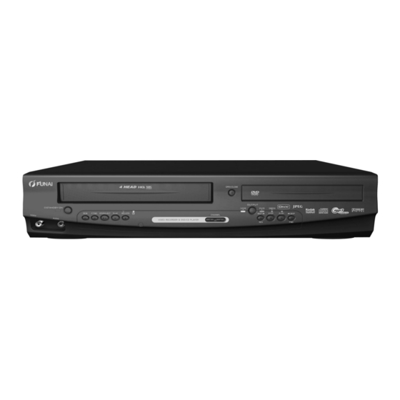
VIDEO CASSETTE RECORDER
DVD PLAYER &
D8B-M1000ZB
D8C-M1000DB
When servicing the deck
mechanism, refer to MK14 Deck
Mechanism Section.
Deck Mechanism Part No.:
N25C0FL
PAL
PAL
SECAM
Advertisement
Table of Contents

Related Manuals for FUNAI D8B-M1000ZB


Summary of Contents for FUNAI D8B-M1000ZB
-
Page 1: Dvd Player
I Specifications mechanism, refer to MK14 Deck I Preparation for Servicing Mechanism Section. I Adjustment Procedures I Schematic Diagrams Deck Mechanism Part No.: I CBA’s I Exploded views N25C0FL I Parts List DVD PLAYER & VIDEO CASSETTE RECORDER D8B-M1000ZB D8C-M1000DB SECAM... -
Page 2: Table Of Contents
MAIN SECTION DVD PLAYER & VIDEO CASSETTE RECORDER D8B-M1000ZB D8C-M1000DB Main Section I Specifications I Preparation for Servicing I Adjustment Procedures I Schematic Diagrams I CBA’s I Exploded Views I Parts List TABLE OF CONTENTS Specifications ............... . . 1-1-1 Laser Beam Safety Precautions . -
Page 3: Specifications
SPECIFICATIONS < VCR Section > Description Unit Minimum Nominal Maximum Remark 1. Video 1-1. Video Output (PB) Vp-p SP Mode 1-2. Video Output (R/P) Vp-p SP Mode, 1-3. Video S/N Y (R/P) W/O Burst 1-4. Video Color S/N AM (R/P) SP Mode 1-5. - Page 4 < DVD Section > ITEM CONDITIONS UNIT NOMINAL LIMIT 75 Ω load 1. Video Output ± 0.1 2. Optical Digital Out 3. Audio (PCM) 1 kHz 0 dB, 47k Ω load 3-1. Output Level Vrms 47k Ω load 3-2. S/N 3-3.
-
Page 5: Laser Beam Safety Precautions
LASER BEAM SAFETY PRECAUTIONS This DVD player uses a pickup that emits a laser beam. Do not look directly at the laser beam coming from the pickup or allow it to strike against your skin. The laser beam is emitted from the location shown in the figure. When checking the laser diode, be sure to keep your eyes at least 30 cm away from the pickup lens when the diode is turned on. -
Page 6: Important Safety Precautions
IMPORTANT SAFETY PRECAUTIONS Product Safety Notice K. When connecting or disconnecting the internal connectors, first, disconnect the AC plug from the Some electrical and mechanical parts have special AC outlet. safety-related characteristics which are often not evi- dent from visual inspection, nor can the protection they give necessarily be obtained by replacing them with components rated for higher voltage, wattage, etc. -
Page 7: Safety Check After Servicing
Safety Check after Servicing Examine the area surrounding the repaired location for damage or deterioration. Observe that screws, Chassis or Secondary Conductor parts, and wires have been returned to their original positions. Afterwards, do the following tests and con- Primary Circuit firm the specified values to verify compliance with safety standards. -
Page 8: Standard Notes For Servicing
STANDARD NOTES FOR SERVICING Circuit Board Indications Pb (Lead) Free Solder When soldering, be sure to use the Pb free solder. 1. The output pin of the 3 pin Regulator ICs is indi- cated as shown. How to Remove / Install Flat Pack-IC Top View Bottom View 1. - Page 9 3. The flat pack-IC on the CBA is affixed with glue, so With Soldering Iron: be careful not to break or damage the foil of each (1) Using desoldering braid, remove the solder from all pin or the solder lands under the IC when removing pins of the flat pack-IC.
- Page 10 2. Installation (4) Bottom of the flat pack-IC is fixed with glue to the CBA; when removing entire flat pack-IC, first apply (1) Using desoldering braid, remove the solder from soldering iron to center of the flat pack-IC and heat the foil of each pin of the flat pack-IC on the CBA up.
- Page 11 Instructions for Handling Semi-conductors Electrostatic breakdown of the semi-conductors may occur due to a potential difference caused by electro- static charge during unpacking or repair work. 1. Ground for Human Body Be sure to wear a grounding band (1MΩ) that is prop- erly grounded to remove any static electricity that may be charged on the body.
-
Page 12: Preparation For Servicing
PREPARATION FOR SERVICING How to Enter the Service Mode About Optical Sensors Caution: An optical sensor system is used for the Tape Start and End Sensors on this equipment. Carefully read and follow the instructions below. Otherwise the unit may operate erratically. What to do for preparation Insert a tape into the Deck Mechanism Assembly and press the PLAY button. -
Page 13: Cabinet Disassembly Instructions
CABINET DISASSEMBLY INSTRUCTIONS 1. Disassembly Flowchart REMOVAL This flowchart indicates the disassembly steps to gain REMOVE/*UNHOOK/ LOC. PART Fig. access to item(s) to be serviced. When reassembling, UNLOCK/RELEASE/ Note follow the steps in reverse order. Bend, route, and UNPLUG/DESOLDER dress the cables as they were originally. 5(S-8), 2(S-9), (S-10), [1] Top Case Chassis Unit... - Page 14 Reference Notes CAUTION 1: Locking Tabs (L-1) and (L-2) are fragile. Be careful not to break them. (S-1) (S-1) 1-1. Release three Locking Tabs (L-1). [1] Top Case 1-2. Release three Locking Tabs (L-2), then remove the Front Assembly. CAUTION 2: Electrostatic breakdown of the laser (S-1) diode in the optical system block may occur as a potential difference caused by electrostatic charge...
- Page 15 CN401 (S-3) CN601 (S-9) (S-8) (S-3) (S-8) [4] DVD Mechanism (S-9) Assembly (S-3) (S-4) [5] Partition Plate (S-8) (S-5) (S-6) CN501 (S-10) [9] VCR Chassis Unit [7] Loader Holder [6] Power Supply CBA (L-3) Fig. D5 Fig. D3 (S-7) (S-7) [8] DVD Main CBA Unit CN301...
- Page 16 Cylinder Assembly FE Head ACE Head Assembly [10] Deck Assembly SW507 Lead with blue stripe LD-SW [13] Jack-A CBA (S-11) (S-13) [12] Main CBA [10] Deck Assembly (S-13) Cam Gear [12] Main CBA Desolder (S-11) Hole Shaft from bottom [11] DVD (S-12) Open/Close CBA Hole...
- Page 17 HOW TO EJECT MANUALLY 1. Remove the Top Case, Front Assembly and Top Bracket. 2. Remove four Screws (S-3) in Fig. D3. Do not disconnect connectors. 3. While lifting up the DVD Mechanism, rotate the roulette in the direction of the arrow as shown below.
-
Page 18: Electrical Adjustment Instructions
ELECTRICAL ADJUSTMENT INSTRUCTIONS General Note: "CBA" is an abbreviation for 3. To check/reset the initial function "Circuit Board Assembly." setting NOTE: Preparation: Electrical adjustments are required after replacing 1. Enter the service mode. circuit components and certain mechanical parts. It is important to do these adjustments only after all repairs 2. -
Page 19: How To Initialize The Dvd Player & Vcr
HOW TO INITIALIZE THE DVD PLAYER & VCR To put the program back at the factory-default, initialize the DVD player & VCR as the following procedure. < DVD Section > 1. Press [DVD], [1], [2], [3], [4], and [DISPLAY] buttons on the remote control unit in that order. Fig. -
Page 20: Firmware Renewal Mode
FIRMWARE RENEWAL MODE 1. Turn the power on and remove the disc on the tray. " ******* " differs depending on the models. 2. To put the DVD player into version up mode, press [DVD], [9], [8], [7], [6], and [SEARCH] buttons on F/W Version Up Mode Model No : ******* the remote control unit in that order. -
Page 21: Function Indicator Symbols
FUNCTION INDICATOR SYMBOLS Note: If a mechanical malfunction occurs, the power is turned off. When the power comes on again after that by pressing [STANDBY-ON] button, an error message is displayed on the TV screen for 5 seconds. MODE INDICATOR ACTIVE When reel or capstan mechanism is not “A R”... -
Page 22: Block Diagrams
BLOCK DIAGRAMS <VCR SECTION> Servo / System Control Block Diagram E8GA1BLS 1-11-1... - Page 23 Video Block Diagram E8GA1BLV 1-11-2...
- Page 24 Audio Block Diagram E8GA1BLA 1-11-3...
- Page 25 Power Supply Block Diagram E8GA1BLP 1-11-4...
- Page 26 BLOCK DIAGRAMS <DVD SECTION> DVD System Control / Servo Block Diagram E8GA1BLSD 1-11-5...
- Page 27 Digital Signal Process Block Diagram E8GA1BLD 1-11-6...
- Page 28 DVD Video / Audio Block Diagram 1-11-7 E8GA1BLVD...
-
Page 29: Schematic Diagrams / Cba's And Test Points
SCHEMATIC DIAGRAMS / CBA’S AND TEST POINTS Standard Notes WARNING Many electrical and mechanical parts in this chassis have special characteristics. These characteristics often pass unnoticed and the protection afforded by them cannot necessarily be obtained by using replacement components rated for higher voltage, wattage, etc. - Page 30 LIST OF CAUTION, NOTES, AND SYMBOLS USED IN THE SCHEMATIC DIAGRAMS ON THE FOLLOWING PAGES: 1. CAUTION: FOR CONTINUED PROTECTION AGAINST FIRE HAZARD, REPLACE ONLY WITH THE SAME TYPE FUSE. 2. CAUTION: Fixed Voltage (or Auto voltage selectable) power supply circuit is used in this unit. If Main Fuse (F1001) is blown, first check to see that all components in the power supply circuit are not defec- tive before you connect the AC plug to the AC power supply.
- Page 31 Main 1/8 Schematic Diagram < VCR Section > Comparison Chart of Models and Marks MODEL MARK D8B-M1000ZB D8C-M1000DB 1-12-3 E8GA1SCM1...
- Page 32 Main 2/8 & Sensor Schematic Diagram < VCR Section > Comparison Chart of Models and Marks MODEL MARK D8B-M1000ZB D8C-M1000DB 1-12-4 E8GA1SCM2...
- Page 33 Main 3/8 Schematic Diagram < VCR Section > Comparison Chart of Models and Marks MODEL MARK D8B-M1000ZB D8C-M1000DB 1-12-5 E8GA1SCM3...
- Page 34 Main 4/8 Schematic Diagram < VCR Section > 1-12-6 E8GA1SCM4...
- Page 35 Main 5/8 Schematic Diagram < VCR Section > 1-12-7 E8GA1SCM5...
- Page 36 Main 6/8 Schematic Diagram < VCR Section > 1-12-8 E8GA1SCM6...
- Page 37 Main 7/8 & DVD Open/Close Schematic Diagram < VCR Section > 1-12-9 E8GA1SCM7...
- Page 38 Main 8/8 Schematic Diagram (B) < VCR Section > Comparison Chart of Models and Marks MODEL MARK D8B-M1000ZB D8C-M1000DB 1-12-10 E8GA2SCM8...
- Page 39 Power Supply & Junction Schematic Diagram < VCR Section > CAUTION ! CAUTION ! NOTE: Fixed voltage (or Auto voltage selectable) power supply circuit is used in this unit. For continued protection against fire hazard, The voltage for parts in hot circuit is measured using If Main Fuse (F1001) is blown , check to see that all components in the power supply hot GND as a common terminal.
- Page 40 Jack - A Schematic Diagram < VCR Section > E8GA1SCJ 1-12-12...
- Page 41 DVD Main 1/3 Schematic Diagram < DVD Section > 1 NOTE: Either IC461 or IC462 is used for DVD MAIN CBA UNIT. 1-12-13 E8GA1SCD1...
- Page 42 DVD Main 2/3 Schematic Diagram < DVD Section > Comparison Chart of Models and Marks MODEL MARK D8B-M1000ZB D8C-M1000DB 1-12-14 E8GA1SCD2...
- Page 43 DVD Main 3/3 Schematic Diagram < DVD Section > 1-12-15 E8GA1SCD3...
- Page 44 Main CBA Top View Sensor CBA Top View BHF300F01012A TP751 TP301 BHF300F01012B V-OUT C-PB TP504 RF-SW TP502 END-S TP501 S-INH 1-12-16 BE8G00F01012A...
- Page 45 Main CBA Bottom View PIN 6 OF IC1403 PIN 16 OF CN1601 PIN 14 OF CN1601 PIN 12 OF CN1601 PIN 10 OF CN1601 PIN 8 OF CN1601 1-12-17 BE8G00F01012A...
- Page 46 DVD Open/Close DVD Open/Close CBA Top View CBA Bottom View BE8G00F01012C Jack -A CBA Bottom View Jack -A CBA Top View BE8G00F01021C 1-12-18...
- Page 47 Power Supply CBA Top View Power Supply CBA Bottom View CAUTION ! Because a hot chassis ground is present in the power CAUTION ! supply circut, an isolation transformer must be used. For continued protection against fire hazard, Fixed voltage (or Auto voltage selectable) power supply circuit is used in this unit. replace only with the same type fuse.
-
Page 48: Waveforms
WAVEFORMS NOTE: Input COLOR BAR SIGNAL (WITH 1KHz AUDIO SIGNAL) TP301 UPPER TP504 Pin 8 of CN1601 Pin 12 of CN1601 LOWER C-PB 0.2V DVD-AUDIO(L) 0.5ms RF-SW VIDEO-Y 0.2V 20µs TP751 UPPER TP504 Pin 10 of CN1601 Pin 14 of CN1601 LOWER V-OUT 0.5V... -
Page 49: Wiring Diagram < Vcr Section
WIRING DIAGRAM < VCR SECTION > 1-14-1 E8GA1WI... -
Page 50: Wiring Diagram < Dvd Section
WIRING DIAGRAM < DVD SECTION > 1-14-2 E8GA1WID... -
Page 51: Ic Pin Function Descriptions
IC PIN FUNCTION DESCRIPTIONS Comparison Chart of Models and Marks Signal Active Mark Function Name Level Model Mark D8B-M1000ZB Head Amp D8C-M1000DB H-A-COMP Comparator Signal < VCR Section > Video Head OUT RF-SW Switching IC501( SERVO / SYSTEM CONTROL IC ) - Page 52 Signal Active Signal Active Mark Function Mark Function Name Level Name Level Main Clock Not Used OUT Xout Input SECAM SECAM-H Vss(GND) Mode at High Not Used Audio IN/ OUT AUDIO- OUT Control SCART 8Pin Signal DVD-8PIN- DVD Input Control Audio IN/ OUT AUDIO- Signal...
- Page 53 Signal Active Mark Function Name Level Loading H/L/ OUT LM-FWD/ Motor Control Hi-z Signal OUT OUTPUT- Output Select SELECT Audio Mute OUT AUDIO- Control MUTE-H Signal (Mute = “H”) Not Used Not Used Not Used Capstan Motor PULSE C-FG Rotation Detection Pulse Not Used...
-
Page 54: Lead Identifications
LEAD IDENTIFICATIONS KRA103M-AT/P 2SA1015-GR(TE2 F T) 2SK3566 KRC103M-AT/P 2SA1020-Y(TE6 F M) SPA02N80C3 KTA1267-(GR,Y)-AT/P 2SA1815-(BL,GR,Y)(TE2 F T) KTA1281Y-AT/P 2SC2120-Y(TE2 F T) KTC3199-(BL,GR,Y)-AT/P 2SC3266-Y(TPE2 F) RN2204(TE4 F T) KTA1266-GR-AT/P KTC3203-Y-AT/P KTC3205-Y-AT/P G D S E C B E C B KIA4558P/P KRC103S-RTK/P FMG4A T148 EL817A BR24L02F-WE2... -
Page 55: Exploded Views
EXPLODED VIEWS Cabinet 2L071 2L071 2B21 2L071 See Electrical Parts List 2L012 for parts with this mark. 2L021 2L021 2L071 Some Ref. Numbers are 2L021 not in sequence. L0-9 L0-9 2L082 JW004 2L020 Jack-A CBA 2L021 JW003 Sensor CBA DVD Main CBA Unit 2B11 2B46... - Page 56 Packing X20A X20B X20C Some Ref. Numbers Unit are not in sequence. Comparison Chart of Models and Marks Model Mark D8B-M1000ZB D8C-M1000DB 1-17-2 E8GA1PEX...
-
Page 57: Mechanical Parts List
1VMN23501 POST CARD E8G00ED 1VMN23493 Comparison Chart of Models and Marks HANDBILL E8G01BD 1VMN23556 QUICK GUIDE(EN) E8GA1BD 1VMN23503 Model Mark D8B-M1000ZB D8C-M1000DB Ref. No. Mark Description Part No. FRONT ASSEMBLY E8GA1BD 1VM222905 FRONT ASSEMBLY E8GA2FD 1VM222906 TOP CASE(BLACK) E8G00ED 1VM323682... -
Page 58: Electrical Parts List
Comparison Chart of Models and Marks C153 CHIP CERAMIC CAP .(1608) F Z 0.1µF/ CHD1JZ30F104 Model Mark 50V or D8B-M1000ZB CHIP CERAMIC CAP .(1608) F Z 0.1µF/ CHD1EZ30F104 D8C-M1000DB C154 CHIP CERAMIC CAP .(1608) F Z 0.1µF/ CHD1JZ30F104 50V or DVD MAIN CBA UNIT CHIP CERAMIC CAP .(1608) F Z 0.1µF/... - Page 59 Ref. No. Mark Description Part No. Ref. No. Mark Description Part No. C311 CHIP CERAMIC CAP .(1608) F Z 0.1µF/ CHD1JZ30F104 C371 CHIP CERAMIC CAP .(1608) B K 0.022µF/ CHD1JK30B223 50V or 50V or CHIP CERAMIC CAP .(1608) F Z 0.1µF/ CHD1EZ30F104 CHIP CERAMIC CAP .(1608) B K 0.022µF/ CHD1EK30B223...
- Page 60 Ref. No. Mark Description Part No. Ref. No. Mark Description Part No. C502 CHIP CERAMIC CAP .(1608) B K 0.022µF/ CHD1JK30B223 C555 CHIP CERAMIC CAP .(1608) B K 0.1µF/ CHD1EK30B104 50V or 25V or CHIP CERAMIC CAP .(1608) B K 0.022µF/ CHD1EK30B223 CHIP CERAMIC CAP .(1608) B K 0.1µF/ CHD1CK30B104...
- Page 61 Ref. No. Mark Description Part No. Ref. No. Mark Description Part No. C1422 CHIP CERAMIC CAP .(1608) B K 0.1µF/ CHD1EK30B104 DIODE ZENER 11BSA-T26 or NDTA011BST26 25V or ZENER DIODE DZ-11BSAT265 NDTA00DZ11BS CHIP CERAMIC CAP .(1608) B K 0.1µF/ CHD1CK30B104 D119 ZENER DIODE MTZJT-7711A or QDTA00MTZJ11...
- Page 62 Ref. No. Mark Description Part No. Ref. No. Mark Description Part No. IC ANALOG MULTIPLEXER NSZBA0TTY093 Q506 PHOTO TRANSISTOR PT204-6B-12 or NPWZT2046B12 CD4053BNSR or PHOTO TRANSISTOR MID-32A22F NPWZ1D32A22F IC ANALOG MULTIPLEXERS NSZBA0TF3138 Q507 TRANSISTOR KTC3199-Y-AT/P or NQSYKTC3199P CD4053BCSJX_NL TRANSISTOR KTC3199-GR-AT/P NQS4KTC3199P IC1002 VOLTAGE REGULATOR...
- Page 63 Ref. No. Mark Description Part No. Ref. No. Mark Description Part No. CARBON RES. 1/6W J 4.7k Ω or RES CHIP 1608 1/10W J 10k Ω R105 RCX6JATZ0472 RRXA103YF002 CARBON RES. 1/4W J 4.7k Ω CHIP RES. 1/10W J 1.2k Ω or RCX4JATZ0472 R323 RRXAJR5Z0122...
- Page 64 Ref. No. Mark Description Part No. Ref. No. Mark Description Part No. RES CHIP 1608 1/10W J 12k Ω CARBON RES. 1/4W J 330 Ω RRXA123YF002 RCX4JATZ0331 CHIP RES. 1/10W J 10k Ω or CHIP RES. 1/10W J 3.9k Ω or R419 RRXAJR5Z0103 R535...
- Page 65 Ref. No. Mark Description Part No. Ref. No. Mark Description Part No. CHIP RES. 1/10W J 1k Ω or RES CHIP 1608 1/10W F 30.0k Ω R705 RRXAJR5Z0102 RTW3002YF002 RES CHIP 1608 1/10W J 1.0k Ω CHIP RES. 1/10W J 1k Ω or RRXA102YF002 R1211 RRXAJR5Z0102...
- Page 66 Ref. No. Mark Description Part No. Ref. No. Mark Description Part No. CHIP RES. 1/10W J 3.9k Ω or R2051 RRXAJR5Z0392 2B46 ROHM HOLDER H7770JD 0VM304573 RES CHIP 1608 1/10W J 3.9k Ω RRXA392YF002 2L062 SCREW B-TIGHT M3X8 BIND HEAD+ GBHB3080 CHIP RES.
- Page 67 POWER SUPPLY CBA Ref. No. Mark Description Part No. DIODE SWITCHING 1N4148-F0021 or NDTZ01N4148F Ref. No. Mark Description Part No. SWITCHING DIODE 1N4148M NDTZ01N4148M POWER SUPPLY CBA (PSV-A) --------- D1008 SCHOTTKY BARRIER DIODE SB140 or NDQZ000SB140 Consists of the following: DIODE SCHOTTKY SB140 or NDLZ00SB140S CAPACITORS...
- Page 68 Ref. No. Mark Description Part No. Ref. No. Mark Description Part No. TRANSISTOR KTA1267-GR-AT/P NQS1KTA1267P TRANS POWER 6708 LTTZPE0KT004 Q1008 TRANSISTOR KTC3199-Y-AT/P or NQSYKTC3199P JUNCTION CBA TRANSISTOR KTC3199-GR-AT/P or NQS4KTC3199P TRANSISTOR 2SC1815-Y(TE2 F T) or QQSY2SC1815F Ref. No. Mark Description Part No.
- Page 69 Ref. No. Mark Description Part No. CARBON RES. 1/4W J 4.7k Ω RCX4JATZ0472 CHIP RES. 1/10W J 75 Ω or R126 RRXAJR5Z0750 RES CHIP 1608 1/10W J 75 Ω RRXA750YF002 MISCELLANEOUS JK1402 RGB CONNECTOR MRC-021V-03 JXGL210LY006 ABS(B11 JW003 FLAT CABLE 10P AWG26#2651/P2.0/190 WX3810S6FF19 JW004 FLAT CABLE 4P AWG26#2651/P2.0/190 WX3804S6FF19...
- Page 70 D8B-M1000ZB/D8C-M1000DB E8GA1BD/2FD 2007-05-14...