Table of Contents
Advertisement
HCD-BX5/DX5/DX5J
SERVICE MANUAL
Ver 1.3 2003.11
• HCD-BX5/DX5/DX5J are the tuner,
deck, CD and amplifier section in
MHC-BX5/DX5/DX5J.
AUDIO POWER SPECIFICATIONS:
(HCD-BX5 US model only)
POWER OUTPUT AND TOTAL
HARMONIC DISTORTION:
with 6 ohm loads both channels driven, from 120-10,000 Hz; rates
95 watts per channel minimum RMS power, with no more than 10%
total harmonic distortion from 250 milliwatts to rated output.
Amplifier section
US, Canadian model:
HCD-BX5:
Continuous RMS power output (reference)
80 + 80 watts
(6 ohms at 1 kHz, 10% THD)
Total harmonic distortion less than 0.07%
(6 ohms at 1 kHz, 50 W)
AEP, UK model:
HCD-BX5:
DIN power output (rated) 80 + 80 watts
(6 ohms at 1 kHz, DIN)
Continuous RMS power output (reference)
100 + 100 watts
(6 ohms at 1 kHz, 10% THD)
Music power output (reference)
170 + 170 watts
(6 ohms at 1 kHz, 10% THD)
Other model:
HCD-DX5:
The following measured at AC 120, 220, 240 V 50/60 Hz
Sony Corporation
9-929-058-14
2003K16-1
Home Audio Company
© 2003.11
Published by Sony Engineering Corporation
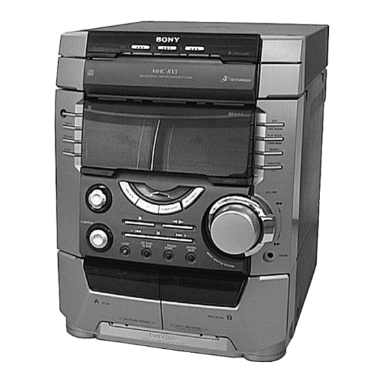
Photo: HCD-BX5
Model Name Using Similar Mechanism
CD
CD Mechanism Type
Section
Base Unit Name
Optical Pick-up Name
Tape deck
Model Name Using Similar Mechanism
Section
Tape Transport Mechanism Type
SPECIFICATIONS
DIN power output (rated) 95 + 95 watts
Continuous RMS power output (reference)
Inputs
MD/VIDEO IN:
(phono jacks)
MIC:
(mini jack)
Outputs
PHONES:
(stereo mini jack)
SPEAKER:
CD player section
System
Laser
Laser output
COMPACT DISC DECK RECEIVER
US Model
Canadian Model
AEP Model
UK Model
HCD-BX5
E Model
Australian Model
HCD-DX5/DX5J
NEW
CDM58-K2BD38
BU-K2BD38
KSM-213D
NEW
TCM-230MWR11
(6 ohms at 1 kHz, DIN)
125 + 125 watts
(6 ohms at 1 kHz, 10% THD)
voltage 450/250 mV,
impedance 47 kilohms
sensitivity 1 mV,
impedance 10 kilohms
accepts headphones of
8 ohms or more
accepts impedance of 6 to 16 ohms
Compact disc and digital audio system
Semiconductor laser (λ=780 nm)
Emission duration: continuous
Max. 44.6 µ W*
*This output is the value measured at a
distance of 200 mm from the objective
lens surface on the Optical Pick-up Block
with 7 mm aperture.
— Continued on next page —
Advertisement
Chapters
Table of Contents

Related Manuals for Sony HCD-BX5


Summary of Contents for Sony HCD-BX5
- Page 1 Canadian Model Ver 1.3 2003.11 AEP Model UK Model HCD-BX5 E Model Australian Model HCD-DX5/DX5J • HCD-BX5/DX5/DX5J are the tuner, deck, CD and amplifier section in MHC-BX5/DX5/DX5J. Photo: HCD-BX5 Model Name Using Similar Mechanism CD Mechanism Type CDM58-K2BD38 Section Base Unit Name...
-
Page 2: Leakage Test
Design and specifications are subject to change without notice. Tape player section Recording system 4-track 2-channel stereo Frequency response 40 – 13,000 Hz (±3 dB), using Sony TYPE I cassette Tuner section SAFETY CHECK-OUT FM stereo, FM/AM superheterodyne tuner (US model only) -
Page 3: Table Of Contents
TABLE OF CONTENTS NOTES ON HANDLING THE OPTICAL PICK-UP BLOCK OR BASE UNIT 1. SERVICE NOTE ······························································· 4 2. GENERAL ·········································································· 5 The laser diode in the optical pick-up block may suffer electrostatic break-down because of the potential difference generated by the 3. - Page 4 SECTION 1 SERVICE NOTE Note for installing the panel board 2 Panel board Hot melt Screw hole 1 Cut the eleven melted-connection points with a cutting plier. Attach the panel board with six screws (+BVTP 2.6 × 8 ) after the board is removed once. Do not tighten the screws excessively.
-
Page 5: General
SECTION 2 GENERAL 2 3 4 Photo: HCD-BX5 DISC SKIP EX-CHANGE button V-GROOVE button and indicator DISC 1 button and indicator CURSOL button and indicator DISC 2 button and indicator GROOVE button DISC 3 button and indicator EQ EDIT button... - Page 6 This section is extracted from instruction manual.
-
Page 7: Disassemby
SECTION 3 DISASSEMBY Note : Follow the disassembly procedure in the numerical order given. 9 Two screws (+BVTP 3 × 10) Upper case (Top) 3-1. UPPER CASE (TOP) 5 Two screws (Case) 7 Two screws (+BVTP 3 × 10) Side panel R Side panel L 6 Screw (Case) 3 Two screws... - Page 8 3-3. FRONT PANEL SECTION CD mechanism deck (CDM58) 4 Screw (+BVTP 3 × 10) 1 Flat type wire (CN304) 5 Screw (+BVTP 3 × 10) 2 Connector (CN1) 3 Connector (CN2) Front panel section 6 Three screws (+BVTT 3 × 6) 3-4.
- Page 9 3-5. PANEL BOARD 8 Three claws 7 Two screws (+BVTP 3 × 10) 9 CD Switch board 2 Two screws qs Panel board (+BVTP 2.6 × 8) qa Five claws 3 Two bosses & four pins 5 FR knob q; Cut the eleven melted-connection points with a cutting plier. 4 Bracket (FR) Note: When attching the panel board, refer to "Service Note"...
- Page 10 3-7. MAIN BOARD AND AMP BOARD 4 Three screws (+BVTP 3 × 10) 7 Heat sink 6 Two screws (+BVTP 3 × 10) 5 Power AMP board 3 Two screws (+BVTP 3 × 10) 2 Main board 1 Two screws (+BVTP 3 × 8) 3-8.
- Page 11 3-9. BASE UNIT 4 Two insulators Base unit 1 Flat type wire (CN101) 5 Two insulators 2 Four screws (+PTPWH 2.6) 3-10. DRIVER BOARD, MOTOR BOARD AND ADDRESS SENSOR BOARD 8 Screw (+PTPWH 2.6 × 8) 5 Three screws (+BVTP 2.6 × 8) 7 Motor board 4 Flat type wire (CN721) q;...
-
Page 12: Test Mode
SECTION 4 TEST MODE [MC Cold Reset] [Change-over of MW Tuner Step between 9 kHz and • The cold reset clears all data including preset data stored in the 10 kHz] RAM to initial conditions. Execute this mode when returning •... - Page 13 [MC Test Mode] • This mode is used to check operations of the respective sections of Amplifier, Tuner, CD and Tape. Procedure: Press the ?/1 button to turn on the set. Press the three buttons of x , ENTER and DISC 3 simultaneously.
- Page 14 [Aging Mode] This mode can be used for operation check of CD section and tape deck section. • If an error occurred: The aging operation stops and display status. • If no error occurs: The aging operation continues repeatedly. 1. Operating method of Aging Mode Turn on the main power and select “CD”...
- Page 15 2) Operation during aging mode In the aging mode, the program is executed in the following sequence. (1) The disc tray opens and closes. (2) The mechanism accesses DISC 2 and makes an attempt to read TOC. However, since there are no discs, a message “CD2 NO DISC”...
-
Page 16: Mechanical Adjustments
SECTION 5 SECTION 6 MECHANICAL ADJUSTMENTS ELECTRICAL ADJUSTMENTS Precaution DECK SECTION 0 dB=0.775 V 1. Clean the following parts with a denatured alcohol-moistened swab: 1. Demagnetize the record/playback head with a head record/playback heads pinch rollers demagnetizer. erase head rubber belts 2. - Page 17 2. Turn the adjustment screw and check output peaks. If the peaks DECK B Tape Speed Adjustment do not match for L-CH and R-CH, turn the adjustment screw Note: Start the Tape Speed adjustment as below after setting to the test so that outputs match within 1dB of peak.
- Page 18 DECK B REC Bias Adjustment 4. Mode: Record Procedure: INTRODUCTION MD/VIDEO (AUDIO) IN When set to the test mode performed in Tape Speed Adjustment, 315 Hz, 50 mV (–23.8 dB) AF OSC when the tape is rewound after recording, the “REC memory mode” blank tape 600 Ω...
- Page 19 FM Tuned Level Adjustment CD SECTION FM RF SSG Note : 1. CD Block is basically designed to operate without adjustment. 75 Ω coaxial Therefore, check each item in order given. 2. Use YEDS-18 disc (3-702-101-01) unless otherwise indicated. 3. Use an oscilloscope with more than 10MΩ impedance. 4.
-
Page 20: Ic101
Note : Clear RF signal waveform means that the shape “ ◊ ” can be clearly Adjustment Location: distinguished at the center of the waveform. [BD BOARD] (Conductor Side) RF signal waveform VOLT/DIV : 200mV TIME/DIV : 500ns level : 1.45 ± 0.3Vp-p E-F Balance (1 Track jump) Check oscilloscope BD board... -
Page 21: Circuit Board Location
HCD-BX5/DX5/DX5J SECTION 7 DIAGRAMS 7-1. CIRCUIT BOARD LOCATION THIS NOTE IS COMMON FOR PRINTED WIRING BOARDS AND SCHEMATIC DIAGRAMS. (In addition to this, the necessary note is printed in each block.) MOTOR Board DRIVER Board Note on Schematic Diagram: Note on Printed Wiring Boards: •... -
Page 22: Ic102
HCD-BX5/DX5/DX5J Ver 1.3 2003.11 7-2. BLOCK DIAGRAMS EXCEPT US,CND,AEP MODEL AM/FM IF MPX TM601 LPF601 TUNER/CD SECTION FE601 Q602 IC601 CF601 CF602 RF IF BUFFER L-CH • R-CH is omitted due to same as L-CH. ANT IN IF OUT FM IF... -
Page 23: Ic302
HCD-BX5/DX5/DX5J MAIN SECTION INPUT SELECT TONE/VOL CONT IC101 IC102 IC501 TM801 TUNER L-CH SECTION IN2A VOL OUT2 POWER SPEAKER Q504,505 Q861 Q821,822 RY801 Q824,825 R CH LOUT MUTE MUTE MUTE MUTE PROTECT SECTION IN2C RELAY CONT Q103 CONT Q862 DETECTOR... -
Page 24: Printed Wiring Board Bd Section
HCD-BX5/DX5/DX5J Ver 1.3 2003.11 7-3. PRINTED WIRING BOARD BD SECTION • See page page 21 for Circuit Boards Location. • Semiconductor Location Ref. No. Location IC101 IC102 IC103 Q101 KSM-213D (Page 26) -
Page 25: Schematic Diagram Bd Section
HCD-BX5/DX5/DX5J Ver 1.3 2003.11 7-4. SCHEMATIC DIAGRAM BD SECTION • See page page 21 for Wavefoms. • See page page 42 for IC Block Diagrams. (KSM-213D) (Page 29) The components identified by Les composants identifiés par mark 0 or dotted line with mark une marque 0 sont critiques 0 are critical for safety. -
Page 26: Printed Wiring Board Main Section
HCD-BX5/DX5/DX5J 7-5. PRINTED WIRING BOARD MAIN SECTION • See page page 21 for Circuit Boards Location. • Semiconductor Location Ref. No. Location (Page 24) (Page 24) D501 D502 D503 D504 D505 D506 D508 D509 D510 D511 D601 D641 D651 D681... -
Page 27: Schematic Diagram Main Section (1/3)
HCD-BX5/DX5/DX5J 7-6. SCHEMATIC DIAGRAM MAIN SECTION (1/3) • See page page 44 for IC Block Diagrams. (Page 29) -
Page 28: Schematic Diagram Main Section (2/3)
HCD-BX5/DX5/DX5J 7-7. SCHEMATIC DIAGRAM MAIN SECTION (2/3) • See page page 21 for Wavefoms. • See page page 40 for IC Pin Function Description. • See page page 44 for IC Block Diagrams. (Page 29) (Page 29) (Page 29) (Page 29) -
Page 29: Schematic Diagram Main Section (3/3)
HCD-BX5/DX5/DX5J 7-8. SCHEMATIC DIAGRAM MAIN SECTION (3/3) • See page page 44 for IC Block Diagrams. (Page 27) (Page 31) (Page 31) (Page 25) (Page 25) (Page 28) (Page 28) (Page 28) (Page 33) - Page 30 HCD-BX5/DX5/DX5J 7-9. PRINTED WIRING BOARD POWER AMP SECTION • See page page 21 for Circuit Boards Location. • Semiconductor Location Ref. No. Location D501 D502 D541 D551 D581 D941 D979 IC501 Q501 Q503 Q504 Q505 Q506 Q551 Q581 Q941 (Page 26)
- Page 31 HCD-BX5/DX5/DX5J 7-10. SCHEMATIC DIAGRAM POWER AMP SECTION (Page 39) (Page 39) The components identified by Les composants identifiés par mark 0 or dotted line with mark une marque 0 sont critiques 0 are critical for safety. pour la sécurité. Replace only with part number Ne les remplacer que par une specified.
-
Page 32: Printed Wiring Board Panel Section
HCD-BX5/DX5/DX5J 7-11. PRINTED WIRING BOARD PANEL SECTION • See page page 21 for Circuit Boards Location. • Semiconductor Location Ref. No. Location D601 D602 D603 D611 D612 D613 D614 D615 D617 D618 D630 D631 D632 IC601 IC602 IC603 IC721 IC722... -
Page 33: Schematic Diagram Panel Section
HCD-BX5/DX5/DX5J 7-12. SCHEMATIC DIAGRAM PANEL SECTION • See page page 21 for Wavefoms. • See page page 41 for IC Pin Function Description. • See page page 43 for IC Block Diagrams. (Page 29) -
Page 34: Printed Wiring Board Leaf Sw Section
HCD-BX5/DX5/DX5J 7-13. PRINTED WIRING BOARD LEAF SW SECTION • See page page 21 for Circuit Boards Location. • Semiconductor Location Ref. No. Location D1001 D1002 IC1001 IC1002 Q1001 (Page 26) (Page 26) (Page 26) -
Page 35: Schematic Diagram Leaf Sw Section
HCD-BX5/DX5/DX5J 7-14. SCHEMATIC DIAGRAM LEAF SW SECTION (Page 28) -
Page 36: Printed Wiring Board Driver Section
HCD-BX5/DX5/DX5J 7-15. PRINTED WIRING BOARD DRIVER SECTION • See page page 21 for Circuit Boards Location. • Semiconductor Location Ref. No. Location D701 IC701 IC711 (Page 26) -
Page 37: Schematic Diagram Driver Section
HCD-BX5/DX5/DX5J 7-16. SCHEMATIC DIAGRAM DRIVER SECTION • See page page 43 for IC Block Diagrams. -
Page 38: Printed Wiring Board Trans Section
HCD-BX5/DX5/DX5J 7-17. PRINTED WIRING BOARD TRANS SECTION • See page page 21 for Circuit Boards Location. • Semiconductor Location Ref. No. Location D971 D972 D973 D974 D975 D976 D977 IC971 Q971 (Page 30) F975 F974 (Page 30) -
Page 39: Schematic Diagram Trans Section
HCD-BX5/DX5/DX5J 7-18. SCHEMATIC DIAGRAM TRANS SECTION (Page 31) US, CIS *F974, F975 5A : CIS *F974 6.3A : EXCEPT EXCEPT *F975 6.3A MY,SP,TW,EA, AUS,E,AR,MX, TH,KR (Page 31) The components identified by Les composants identifiés par mark 0 or dotted line with mark une marque 0 sont critiques 0 are critical for safety. -
Page 40: Ic Pin Function Description
7-19. IC PIN FUNCTION DESCRIPTION • MAIN BOARD IC401 M30622MAA-A25FP (MASTER CONTROL) Pin No. Pin Name Description Pin No. Pin Name Description SURROUND 1 Not used. Not used. SURROUND 2 Not used. Not used. SURROUND 3 Not used. Not used. 498-DATA Data signal output for IC101 (M61504FP) Not used. - Page 41 • PANEL BOARD IC601 TMP88CP77F-1A22 (DISPLAY CONTROL) Pin No. Pin Name Description VOLUME A VOLUME A signal input. VOLUME B VOLUME B signal input. HEADPHONE Head phone detect signal input. H=ON, L=OFF Not used. TUNER TUNER LED driver output.(high active) CD LED driver output.(high active) TAPE A/B TAPE A/B LED driver output.(high active)
-
Page 42: Ic Block Diagrams
7-20. IC BLOCK DIAGRAMS IC101 CXD2587Q (BD BOARD) ERROR DIGITAL ASYMMETRY DIGITAL CORRECTOR CORRECTION LRCK OPERATIONAL AMPLIFIER PCMD INTERFACE DEMODULATOR ANALOG SWITCH CONVERTER EMPH XVDD CLOCK XTSL GENERATOR XTAI TIMING TES1 LOGIC XTAO TEST XVSS SERVO DSP PWM GENERATOR AVDD1 FRDR FOCUS FOCUS PWM... - Page 43 IC103 CXA2568M (BD BOARD) IC602 BA3830F (PANEL BOARD) APC PD AMP REFFERENCE RESET 18 RESET LC/PD CURRENT LD_ON HOLD REFFERENCE 17 f01 CURRENT AGCVTH VREF APC LD AMP HOLD_SW LINE 16 f02 AGCCONT (50%/30% OFF) LINE RF_BOT 15 f03 RFTC RF SUMMING AMP RF_EQ_AMP RF_1...
- Page 44 IC601 BA1450 (MAIN BOARD) AM IF VREG DECODER DRIVER COMP µPC1330H (MAIN BOARD) IC302 IC681 M5218AFP (MAIN BOARD) INVERTER V– COMPARATER SW R1 SW P1 CONT SW P2 SW R2 IC651 LC72130 (MAIN BOARD) SWALLOW COUNTER 1/16.1/17 4bits POWER REFERENCE RESET DIVIDER SWALLOW COUNTER...
-
Page 45: Main Section
SECTION 8 EXPLODED VIEWS NOTE: • -XX, -X mean standardized parts, so they may • Abbreviation : Mexican model have some differences from the original one. CND : Canadian model : Argentina model • Items marked “*” are not stocked since they : Australian model are seldom required for routine service. -
Page 46: Panel Section
X-4952-419-1 TC HOLDER (R) ASSY 4-224-561-01 BRACKET (HEART CAM R) 4-225-032-01 VOL KNOB 4-225-053-01 SPRING R A-4428-077-A CD SWITCH BOARD,COMPLETE 4-224-584-01 HOLDER (FL) 4-962-708-71 EMBLEM (4-A), SONY A-4428-075-A PANEL BOARD,COMPLETE (AED,AEP,CIS,CND,UK,G,US) 4-225-033-01 FR KNOB X-4952-415-1 FRONT PANEL ASSY (AED,AEP,CIS,UK,G) A-4428-092-A PANEL BOARD,COMPLETE... -
Page 47: Main Board Section
8-3. MAIN BOARD SECTION US, CND T972 not supplied UK,G E,MX,TH EA,MY,SP,TW CIS,AED,AEP,EA,MY,SP,TW not supplied Ref. No. Part No. Description Remarks Ref. No. Part No. Description Remarks 1-773-045-11 WIRE (FLAT TYPE) (17 CORE) A-4428-094-A POWER AMP BOARD,COMPLETE A-4428-070-A MAIN BOARD,COMPLETE (AED,AEP,CIS,UK,G) (AR,AUS,E,EA,KR,MX,MY,SP,TW) A-4428-084-A MAIN BOARD,COMPLETE (CND,US) A-4428-336-A POWER AMP BOARD,COMPLETE (CND) - Page 48 8-4. TAPE MECHANISM DECK SECTION Note: Two different types of tape mechanism are used depending on models. They maintain compatibility as an entire mechanism even though there are some different parts are used. Ref. No. Part No. Description Remarks Ref. No. Part No.
-
Page 49: Cd Mechanism Deck Section
Ver 1.3 2003.11 8-5. CD MECHANISM DECK SECTION Ref. No. Part No. Description Remarks Ref. No. Part No. Description Remarks 4-933-134-11 SCREW (+PTPWH M2.6X8) 4-221-682-01 LEVER (LIFTER) 4-221-679-01 CAM(RELAY) 4-221-688-01 PULLEY (B), CHUCKING 4-221-675-01 TABLE 1-471-035-11 MAGNET ASSY 4-221-686-01 LEVER (CHANGE) X-4952-019-1 PULLEY (A) ASSY, CHUCKING 4-221-676-01 TRAY X-4951-889-1 HOLDER (BU) ASSY... -
Page 50: Electrical Parts List
SECTION 9 ADDRESS SENSOR ELECTRICAL PARTS LIST NOTE: • Due to standardization, replacements in the • COILS : Mexican model uH: µH parts list may be different from the parts : Argentina model specified in the diagrams or the components •... - Page 51 DRIVER HEAD (A) HEAD (B) MAIN Ref. No. Part No. Description Remarks Ref. No. Part No. Description Remarks < RESISTOR > < DIODE > R101 1-216-077-91 RES-CHIP 1/10W D701 8-719-983-63 DIODE MTZJ-T-72-3.3B R102 1-216-097-91 RES-CHIP 100K 1/10W R103 1-216-077-91 RES-CHIP 1/10W <...
- Page 52 MAIN Ref. No. Part No. Description Remarks Ref. No. Part No. Description Remarks C111 1-163-018-00 CERAMIC CHIP 0.0056uF 5% C301 1-126-960-11 ELECT 20.00% 50V C112 1-126-961-11 ELECT 2.2uF 20.00% 50V C302 1-130-479-00 MYLAR 0.0047uF 5% C113 1-126-961-11 ELECT 2.2uF 20.00% 50V C303 1-136-165-00 MYLAR 0.1uF...
- Page 53 MAIN Ref. No. Part No. Description Remarks Ref. No. Part No. Description Remarks C371 1-163-131-00 CERAMIC CHIP 390PF C625 1-163-125-00 CERAMIC CHIP 220PF C372 1-163-117-00 CERAMIC CHIP 100PF (CND,US,AR,AUS,E,EA,KR,MX,MY,SP,TH,TW) C373 1-136-157-00 MYLAR 0.022uF 5.00% 50V C625 1-163-137-00 CERAMIC CHIP 680PF C374 1-126-964-11 ELECT 10uF...
- Page 54 MAIN Ref. No. Part No. Description Remarks Ref. No. Part No. Description Remarks C689 1-163-135-00 CERAMIC CHIP 560PF < FILTER > (AED,AEP,CIS,G,UK) C690 1-126-961-11 ELECT 2.2uF 20.00% 50V CF601 1-760-023-11 FILTER, CERAMIC (AED,AEP,CIS,G,UK) (CND,US,AR,AUS,E,EA,KR,MX,MY,SP,TH,TW) C691 1-163-031-11 CERAMIC CHIP 0.01uF CF601 1-579-185-21 FILTER, CERAMIC (AED,AEP,CIS,G,UK) (AED,AEP,CIS,G,UK) CF602...
- Page 55 MAIN Ref. No. Part No. Description Remarks Ref. No. Part No. Description Remarks < FERRITE BEAD > JR12 1-216-296-91 SHORT JR13 1-216-296-91 SHORT FB201 1-216-295-91 SHORT JR14 1-216-296-91 SHORT FB202 1-216-295-91 SHORT JR15 1-216-296-91 SHORT FB203 1-216-295-91 SHORT JR16 1-216-295-91 SHORT FB204 1-216-295-91 SHORT FB416...
- Page 56 MAIN Ref. No. Part No. Description Remarks Ref. No. Part No. Description Remarks JR910 1-216-295-91 SHORT 0 (AED,AEP,CIS,CND,G,UK,US) Q821 8-729-120-28 TRANSISTOR 2SC1623-T1-L5L6 JR928 1-216-295-91 SHORT 0 (AR,AUS,E,EA,KR,MX,MY,SP,TW) Q822 8-729-120-28 TRANSISTOR 2SC1623-T1-L5L6 JR923 1-216-295-91 SHORT Q823 8-729-216-22 TRANSISTOR 2SA812-T1-M5M6 JR924 1-216-295-91 SHORT Q824 8-729-113-13 TRANSISTOR FA1A4M-T1L33...
- Page 57 MAIN Ref. No. Part No. Description Remarks Ref. No. Part No. Description Remarks R155 1-216-097-91 RES-CHIP 100K 1/10W R340 1-216-107-00 METAL CHIP 270K 1/10W (TH) R341 1-216-033-00 METAL CHIP 1/10W R157 1-216-105-91 RES-CHIP 220K 1/10W R342 1-216-075-00 METAL CHIP 1/10W R158 1-216-097-91 RES-CHIP 100K...
- Page 58 MAIN Ref. No. Part No. Description Remarks Ref. No. Part No. Description Remarks R429 1-216-025-91 RES-CHIP 1/10W R548 1-216-073-00 METAL CHIP 1/10W R430 1-216-025-91 RES-CHIP 1/10W R566 1-216-073-00 METAL CHIP 1/10W R432 1-216-025-91 RES-CHIP 1/10W R601 1-216-295-91 SHORT 0 (EXCEPT US,CND) R433 1-216-025-91 RES-CHIP 1/10W...
- Page 59 MAIN MOTOR Ref. No. Part No. Description Remarks Ref. No. Part No. Description Remarks R683 1-216-097-91 RES-CHIP 100K 1/10W < COMPOSITION CIRCUIT BLOCK > (AED,AEP,CIS,G,UK) R684 1-216-097-91 RES-CHIP 100K 1/10W RB641 1-234-457-11 ENCAPSULATED COMPONENT (AED,AEP,CIS,G,UK) R685 1-216-067-00 METAL CHIP 5.6K 1/10W <...
- Page 60 PANEL Ref. No. Part No. Description Remarks Ref. No. Part No. Description Remarks A-4428-075-A PANEL BOARD, COMPLETE C670 1-162-282-31 CERAMIC 100PF (AED,AEP,CIS,CND,G,UK,US) C671 1-162-282-31 CERAMIC 100PF C717 1-126-157-11 ELECT 10uF ********************** A-4428-092-A PANEL BOARD, COMPLETE (AR,AUS,E,EA,KR,MX,MY,SP,TH,TW) (AR,AUS,E,KR,MX,MY,SP,TW) C718 1-126-157-11 ELECT 10uF (AR,AUS,E,EA,KR,MX,MY,SP,TH,TW) **********************...
- Page 61 PANEL Ref. No. Part No. Description Remarks Ref. No. Part No. Description Remarks C760 1-162-282-31 CERAMIC 100PF < JACK > C761 1-162-282-31 CERAMIC 100PF C762 1-162-282-31 CERAMIC 100PF J631 1-785-569-11 JACK (SMALL TYPE)(PHONE) C763 1-162-282-31 CERAMIC 100PF J721 1-785-569-11 JACK (SMALL TYPE)(MIC 1) C764 1-162-282-31 CERAMIC 100PF...
- Page 62 PANEL Ref. No. Part No. Description Remarks Ref. No. Part No. Description Remarks R635 1-249-401-11 CARBON 1/4W F R723 1-249-433-11 CARBON 1/4W R636 1-249-441-11 CARBON 100K 1/4W (EA) R637 1-249-441-11 CARBON 100K 1/4W R724 1-249-433-11 CARBON 1/4W R638 1-249-441-11 CARBON 100K 1/4W (EA)
- Page 63 PANEL CD SWITCH POWER AMP Ref. No. Part No. Description Remarks Ref. No. Part No. Description Remarks S620 1-762-875-21 SWITCH, KEYBOARD (PAUSE) < SWITCH > S621 1-762-875-21 SWITCH, KEYBOARD (-AMS) S623 1-762-875-21 SWITCH, KEYBOARD (LEFT) S642 1-762-875-21 SWITCH, KEYBOARD (DISC SKIP) S624 1-762-875-21 SWITCH, KEYBOARD (RIGHT) S643...
- Page 64 POWER AMP SUB-TRANS Ref. No. Part No. Description Remarks Ref. No. Part No. Description Remarks < DIODE > R553 1-249-414-11 CARBON 1/4W F R554 1-249-438-11 CARBON 1/4W D501 8-719-911-19 DIODE 1SS133T-72 R555 1-249-417-11 CARBON 1/4W F D502 8-719-911-19 DIODE 1SS133T-72 R556 1-249-431-11 CARBON 1/4W...
- Page 65 Ver 1.3 2003.11 SUB-TRANS TRANS Ref. No. Part No. Description Remarks Ref. No. Part No. Description Remarks < RESISTOR > MISCELLANEOUS ************** R974 1-249-441-11 CARBON 100K 1/4W R975 1-249-429-11 CARBON 1/4W M961 1-763-072-11 FAN, D.C. (AR,AUS,E,EA,KR,MX,MY,SP,TH,TW) 1-773-045-11 WIRE (FLAT TYPE) (17 CORE) <...
- Page 66 HCD-BX5/DX5/DX5J REVISION HISTORY Clicking the version allows you to jump to the revised page. Also, clicking the version at the upper right on the revised page allows you to jump to the next revised page. Ver. Date Description of Revision 2000.01...