Table of Contents
Advertisement
BD Home Theater System
Service
Service
Service
Service Manual
©
Copyright 2010 Philips Consumer Electronics B.V. Eindhoven, The Netherlands
All rights reserved. No part of this publication may be reproduced, stored in a retrieval system or
transmitted, in any form or by any means, electronic, mechanical, photocopying, or otherwise
without the prior permission of Philips.
Published by
KC-RL1047 AVM
Service Audio Printed in The Netherlands Subject to modification
Version 1.3
TABLE OF CONTENTS
Location Of PCB Boards............................................ 1-2
Versions Variation ...................................................... 1-2
Specifications ............................................................ 1-3
Measurement Setup .................................................. 1-4
Service Aids .............................................................. 1-5
ESD & Safety Instruction .......................................... 1-6
Lead-free Soldering Information ................................ 1-7
Setting Procedure & Repair Instructions ...................... 2
Disassembly Instructions, Service Positions & Bly-ray
Loader Mechanism Handling ........................................ 3
Quick Start Guide .......................................................... 4
Block & Wiring Diagram ................................................ 5
VFD Board .................................................................... 6
Main+MP3+Led+Support1+Support2 Board ................ 7
Power Board .................................................................. 8
BD Board........................................................................ 9
Touch Board ................................................................ 10
AMP+USB Board ........................................................ 11
Mechanical Exploded &Packing View ........................ 12
Revision List ................................................................ 13
1 - 1
Chapter
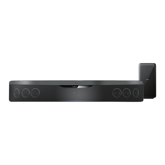
HTS7140
/12/98/93/51/78
3139 785 35403
GB
Advertisement
Table of Contents

Related Manuals for Philips HTS7140/12


Summary of Contents for Philips HTS7140/12
- Page 1 Revision List ..............13 © Copyright 2010 Philips Consumer Electronics B.V. Eindhoven, The Netherlands All rights reserved. No part of this publication may be reproduced, stored in a retrieval system or transmitted, in any form or by any means, electronic, mechanical, photocopying, or otherwise without the prior permission of Philips.
-
Page 2: Location Of Pcb Boards
1 - 2 LOCATION OF PCB BOARDS MAIN POWER VERSION VARIATION: Type/Versions HTS7140 Features Output Power - 500W Voltage (110-127V) Voltage (220-240V) MP3 LINK REPAIR SCENARIO MATRIX: Type/Versions HTS7140 Board in used Main+MP3+Led+Support1+Support2 Board Power Board VFD Board BD Board Touch Board AMP+USB Board *Bd = Board Level Replacement... -
Page 3: Specifications
1 - 3 SPECIFICATIONS Playback media Main Unit AVCHD, BD-RE, BD-Video, DVD-Video, DVD+R/+RW, Power supply ................DVD-R/-RW, DVD+R/-R DL, CD-R/CD-RW, Audio CD, Video Europe/China/Russia/India ... 220-240V, ~50 Hz; (for:/12/51/93) CD/SVCD, Picture CD, MP3-CD, WMA-CD, DivX (Ultra)-CD, Latin America/Asia Pacifi c ..... 110-127V/220-240V, USB storage device ............... - Page 4 1 - 4 MEASUREMENT SETUP Tuner FM Bandpass LF Voltmeter 250Hz-15kHz e.g. PM2534 e.g. 7122 707 48001 RF Generator e.g. PM5326 S/N and distortion meter e.g. Sound Technology ST1700B Use a bandpass filter to eliminate hum (50Hz, 100Hz) and disturbance from the pilottone (19kHz, 38kHz). Use Audio Signal Disc SBC429 4822 397 30184 (replaces test disc 3)
- Page 5 1 - 5 SERVICE AIDS Service Tools: Universal Torx driver holder .........4822 395 91019 Torx bit T10 150mm ...........4822 395 50456 Torx driver set T6-T20 .........4822 395 50145 Torx driver T10 extended ........4822 395 50423 Compact Disc: SBC426/426A Test disc 5 + 5A ......4822 397 30096 SBC442 Audio Burn-in test disc 1kHz ....4822 397 30155 SBC429 Audio Signals disc .........4822 397 30184 Dolby Pro-logic Test Disc ........4822 395 10216...
- Page 6 1 - 6 WAARSCHUWING WARNING Alle IC’s en vele andere halfgeleiders zijn All ICs and many other semi-conductors are gevoelig voor electrostatische ontladingen susceptible to electrostatic discharges (ESD). (ESD). Careless handling during repair can reduce life Onzorgvuldig behandelen tijdens reparatie kan drastically.
- Page 7 • You will find this and more technical information Use only lead-free solder alloy Philips SAC305 with within the “magazine”, chapter “workshop news”. order code 0622 149 00106. If lead-free solder-paste is required, please contact the manufacturer of your For additional questions please contact your local solder-equipment.
- Page 8 (if 1) Restore factory setting 5) Upgrading new software available) on the Philips web site, and for BD-Live application and Do not switch off! a) Press “ ” <Home> button on R/C.
- Page 9 2 - 2 2 - 2 e) Select <Start>, press <OK> button on R/C. 6) OSD Language setup (only for 51 version) 7) Produce to change Tuner grid (only for /98/51 version) In some countries, you can switch the FM tuning grid between 50 Software upgrade will take 5 minutes a) Press “...
- Page 10 2 - 3 2 - 3 REPAIR INSTRUCTIONS (One)
- Page 11 3 - 1 3 - 1 Disassembly Instructions, Service Positions and Blu-ray Loader Mechanism Dismantling of the Blu-ray Loader 1) Loosen 4 screws “D” at the Blu-ray Loader as shown in fi gure 5. handling Dismantling of the Front Assembly 1) According to fi gure 1, the mark to remove wire cover left &...
- Page 12 3 - 2 3 - 2 Dismantling of the Bd Board Dismantling of the AMP Board 1) Loosen 4 screws “K” as shown in fi gure 12. 1) Loosen 4 screws “O” on the bottom of AMP Bard as shown in fi gure 16. 2) Loosen 4 screws “L”...
-
Page 13: Service Positions
3 - 3 3 - 3 Service Positions Service Position C – VFD, AMP & Power Board Service Position A - PCBA Bracket_Vertical Service Position B - AMP & Power Board Service Position D – All Boards Note:In some service positions the components or copper patterns of one board may risk touching its neighbouring pc boards or metallic parts. - Page 14 3 - 4 3 - 4 Blu-ray Loader mechanism handling > Hold by the top and bottom: this holding method may cause damage of chassis since aluminum chassis is used and not recommended. Note: Bottom chassis of BD-LN150 is steel. Note: This Manual describes how to handle TEAC BD-LN150 drives to prevent the unnecessary damages to the drives.
- Page 15 3 - 5 3 - 5 > The other example of bad handling while inserting / ejecting a disc. 4) How to mount BD-LN150. > Utilize Self tap screw holes on the front and rear. > Do not use double side tape to fi x it. It may cause frame deformation when it is removed. 5) Application notes and design recommendation in mounting.
-
Page 16: Quick Start Guide
QUICK START GUIDE The following excerpt of the QSG/DFU serves as an introduction to the set. The complete Direction for Use can be download in the different languages from the internet site of Philips Consumer care Center: www.support.philips.com User Manual... - Page 17 4 - 2 4 - 2 HDMI HDMI Asia Pacific and Latin America only Latin America only SUBWOOFER 110 - 127 V 220 - 240V Antenna HDMI Cable...
- Page 18 4 - 3 4 - 3 HDMI HOME THEATER...
- Page 19 4 - 4 4 - 4 Link Cable USB 2.0 Wi-Fi...
- Page 20 4 - 5 4 - 5 DOCK for iPod Philips DCK3060...
- Page 21 4 - 6 4 - 6 SpeciFI cations are subject to change without notice Trademarks are the property of Koninklijke Philips Electronics N.V. or their respective owners 2010 © Koninklijke Philips Electronics N.V. All rights reserved. sgythy_1018/12/98/51/93/78/v1...
- Page 22 5 - 1 5 - 1 BLOCK DIAGRAM...
- Page 23 5 - 2 5 - 2 WIRING DIAGRAM...
-
Page 24: Vfd Board
6 - 1 6 - 1 FTD DISPLAY PIN ASSIGNMENT VFD BOARD TABLE OF CONTENTS FTD Display Pin Assignment ............. 6-1 Circuit Diagram ................. 6-2 PCB Layout Top & Bottom View ............6-3 PIN CONNECTION... - Page 25 6 - 2 6 - 2 CIRCUIT DIAGRAM C2001 FB2016 C2002 FB2017 C2003 IC2001 C2004 Q2001 C2005 Q2002 C2006 Q2003 C2007 Q2005 C2008 Q2006 C2009 R2001 C2010 R2002 C2011 R2003 C2012 R2004 C2013 R2005 C2014 R2006 C2015 R2007 C2016 R2008 C2017 R2009 C2018...
- Page 26 6 - 3 6 - 3 PCB LAYOUT - TOP VIEW C2001 A1 C2005 A1 C2009 A2 C2013 A2 C2017 A2 C2021 A1 CN2003 A2 FB2002 A2 FB2006 A2 FB2011 A2 FB2016 A2 Q2002 A2 R2001 A1 R2005 A1 R2009 A1 R2014 A2 R2018 A1 R2022 A2...
-
Page 27: Main+Mp3+Led+Support1+Support2 Board
7 - 1 7 - 1 INTERNAL IC DIAGRAM - CS495313 Paral i el Ser i al Ser i al D eoug Cont r ol U ART G PIO Cont r ol 1 Cont r ol 2 12Ch,Audio In/ 6Ch,SACD In 32-b it 32-b it TMR1... - Page 28 7 - 2 7 - 2 CIRCUIT DIAGRAM C1003 B1 C1038 C2 C111 C205 C2065 C4 C220 C241 C302 C318 C334 C352 C398 C946 D1004 D4 FB201 A4 FB302 D1 FB4015 C4 IC305 C1 Q101 R1014 A1 R106 R1092 A1 R138 R154 R171...
- Page 29 7 - 3 7 - 3 PCB LAYOUT - TOP VIEW C101 C107 C2055 C258 C313 C333 C352 C398 CN102 C2 D1007 FB215 FB4012 A3 IC2902 A3 Q105 R1017 R1069 R1097 R146 R167 R187 R205 R248 R308 R324 R340 R3524 R375 R5040 XL101...
- Page 30 7 - 4 7 - 4 PCB LAYOUT - BOTTOM VIEW C1003 C2 C105 B3 C1055 C4 C145 B3 C2059 A4 C2063 A3 C2068 A3 C211 B2 C217 B2 C222 B1 C232 A3 C3004 A1 C346 A1 D203 B2 L1006 A1 R1073 C3 R150 B3 R178 B2...
-
Page 31: Power Board
8 - 1 8 - 1 INTERNAL IC DIAGRAM - AZ431 CATHODE POWER BOARD ANODE TABLE OF CONTENTS Internal IC Diagram ................8-1 Circuit Diagram .................. 8-2 PCB Layout Top View ............... 8-3 PCB Layout Bottom View ..............8-4... - Page 32 8 - 2 8 - 2 CIRCUIT DIAGRAM BD901 A1 C913 C923 C933 C948 C960 C970 C980 CN902 A1 D907 F901 IC906 NTC901 C1 Q910 R904 R914 R925 R935 R947 R957 R967 R977 R988 R998 ZD903 A3 C903 C914 C924 C934 C950 C961...
- Page 33 8 - 3 8 - 3 PCB LAYOUT - TOP VIEW BD901 C916 C925 C934 C946 C967 C978 CN905 D911 IC902 J904 J910 J916 J922 J929 L906 Q914 R911 R957 R981 T902 C903 C917 C926 C941 C950 C968 C980 CN906 D912 IC902 J905...
- Page 34 8 - 4 8 - 4 PCB LAYOUT - BOTTOM VIEW C907 C919 C947 C956 C971 C983 D903 IC901 A2 Q905 A3 Q912 B3 R908A B3 R918 R927 R937 R946 R953 R961 R971 R980 R989 R998 C910 C920 C948 C957 C974 C984 D904...
-
Page 35: Table Of Contents
9 - 1 9 - 1 BD BOARD TABLE OF CONTENTS Circuit Diagram (one) ................ 9-2 Circuit Diagram (two) ................ 9-3 Circuit Diagram (three) ..............9-4 Circuit Diagram (four) ............... 9-5 Circuit Diagram (fi ve) ................ 9-6 Circuit Diagram (six) ................. 9-7 Circuit Diagram (seven) .............. -
Page 36: Circuit Diagram (One)
9 - 2 9 - 2 CIRCUIT DIAGRAM (one) C966 B2 CB12 A3 CE19 A2 CE23 B2 FB710 B1 FB722 B3 FB742 A1 Q519 B2 R473 A2 R478 B2 U908 B2 C960 A2 C971 B2 CB13 A1 CE24 B3 D201 C2 FB712 B2 FB723 B3 FB743 A1... -
Page 37: Circuit Diagram (Two)
9 - 3 9 - 3 CIRCUIT DIAGRAM (two) C100 C104 C108 C112 C116 C120 C124 C128 C132 C136 C140 C144 C148 C152 C970 R101 R105 RN100 B3 RN104 C3 U102 C101 C105 C109 C113 C117 C121 C125 C129 C133 C137 C141 C145... -
Page 38: Circuit Diagram (Three)
9 - 4 9 - 4 CIRCUIT DIAGRAM (three) C200 C203 C206 C209 C212 C215 C218 C221 C224 C227 C230 C233 C236 C239 R202 R205 RN201 B3 RN204 B3 U202 C201 C204 C207 C210 C213 C216 C219 C222 C225 C228 C231 C234 C237... -
Page 39: Circuit Diagram (Four)
9 - 5 9 - 5 CIRCUIT DIAGRAM (four) C300 C309 C316 C322 C330 C906 C911 FB301 FB306 FB311 Q517 R305 R312 R317 R323 R334 R484 Y301 C302 C310 C317 C325 C332 C907 C967 FB302 FB307 FB312 R300 R306 R313 R319 R330 R335... -
Page 40: Circuit Diagram (Fi Ve)
9 - 6 9 - 6 CIRCUIT DIAGRAM (fi ve) C351 C356 C361 C374 CE10 FB352 FB356 J903 R350 R355 R363 R369 R376 R415 R427 R489 U905 C353 C357 C363 C375 CE11 FB353 FB357 Q401 R351 R358 R365 R370 R377 R416 R486 RN350 B1... -
Page 41: Circuit Diagram (Six)
9 - 7 9 - 7 CIRCUIT DIAGRAM (six) C386 C956 FB360 R393 R398 R401 R405 R419 R495 R677 C388 FB358 HA501 C2 R394 R399 R402 R407 R423 R496 C389 FB359 J355 R397 R400 R404 R412 R424 R497... -
Page 42: Circuit Diagram (Seven)
9 - 8 9 - 8 CIRCUIT DIAGRAM (seven) C390 C392 C394 C396 C398 C400 C402 C404 C406 C408 C410 C412 C414 C416 C418 C420 C422 C424 R425 C391 C393 C395 C397 C399 C401 C403 C405 C407 C409 C411 C413 C415 C417 C419... -
Page 43: Circuit Diagram (Eight)
9 - 9 9 - 9 CIRCUIT DIAGRAM (eight) C455 C460 C465 D451 FB501 L453 P502 Q513 R461 R559 C456 C463 C466 CN203 A3 D454 L450 L455 Q511 Q514 R467 C459 C464 C501 D450 D455 L451 P501 Q512 R455 R470... -
Page 44: Circuit Diagram (Nine)
9 - 10 9 - 10 CIRCUIT DIAGRAM (nine) HA500 A3... -
Page 45: Circuit Diagram (Ten)
9 - 11 9 - 11 CIRCUIT DIAGRAM (ten) C700 C704 C708 C713 C905 R498 R502 R506 R510 R514 R518 R522 R526 R536 R544 Y302 C701 C705 C709 C714 FB700 R499 R503 R507 R511 R515 R519 R523 R531 R537 R547 C702 C706 C711... -
Page 46: Circuit Diagram (Eleven)
9 - 12 9 - 12 CIRCUIT DIAGRAM (eleven) C801 A2 C804 A2 C808 A3 C811 B1 C815 B1 C818 B1 C822 B1 C830 B3 C833 B3 C836 B3 C842 B3 C903 A2 C918 A2 C927 B1 R555 A1 R558 A3 R565 B3 R568 B1 R576 B3... -
Page 47: Circuit Diagram (Twelve)
9 - 13 9 - 13 CIRCUIT DIAGRAM (twelve) R622 A1 R659 C2 R683 A1 R684... -
Page 48: Pcb Layout Top View
9 - 14 9 - 14 PCB LAYOUT - TOP VIEW C148 C231 C464 C715 C962 CE18 D1 CN203 D4 FB710 C3 J800 Q511 R105 R309 R363 R473 R502 R514 R542 R584 RN202 D2 U201 Y300 C129 C149 C232 C334 C465 C716 C965... -
Page 49: Pcb Layout Bottom View
9 - 15 9 - 15 PCB LAYOUT - BOTTOM VIEW C100 C112 C124 C137 C204 C216 C238 C315 C353 C388 C411 C423 C803 C819 C901 C923 D201 FB310 C3 FB360 A1 Q401 C1 R326 R358 R412 R478 R535 R577 C101 C113 C125... -
Page 50: Touch Board
10 - 1 10 - 1 TOUCH BOARD TABLE OF CONTENTS Circuit Diagram .................. 10-2 PCB Layout Top & Bottom View ............10-3... - Page 51 10 - 2 10 - 2 CIRCUIT DIAGRAM C11 B2 C13 B2 IC1 A2 R11 B1 R13 B1 R15 B2 R17 A2 R19 B2 R20 A2 R22 A2 C10 B2 C12 B2 R10 B1 R12 B1 R14 B2 R16 B2 R18 B2 R21 A2 R24 A1...
- Page 52 10 - 3 10 - 3 PCB LAYOUT - TOP VIEW PCB LAYOUT - BOTTOM VIEW C11 A1 C13 A1 IC1 A1 R11 A1 R13 A1 R15 A3 R17 A1 R19 A1 R20 A1 R22 A1 C10 A1 C12 A1 R10 A1 R12 A1 R14 A3...
-
Page 53: Amp+Usb Board
11 - 1 11 - 1 INTERNAL IC DIAGRAM - TAS5508BPAG Power Supply MCLK PWM_M PP and MR XTL_OUT Se cti on PWM_M PP and ML XTL_IN Sof t Sof t Loud C om p DRC Em ph Int e rpol at e SRC N S PWM D et Bl quads Tone... - Page 54 11 - 2 11 - 2 CIRCUIT DIAGRAM C4113 A1 C4126 A2 C4171 A1 C5017 B1 C5081 B3 C5111 C1 C5124 B1 C5205 C2 C5218 C2 C5231 C1 C5312 C2 C5325 B2 IC4101 A1 L5106 B1 Q4151 A1 R4106 A1 R4119 A2 R5002 C3 R5043 C3...
- Page 55 11 - 3 11 - 3 PCB LAYOUT - TOP VIEW C4101 D2 C5082 C1 C5331 B1 R4107 D3 R5082 B1 C4102 D2 C5083 A1 C5332 C2 R4108 D2 R5083 C1 C4103 D2 C5101 C3 CN5001 C1 R4111 D2 R5084 C1 C4104 D2 C5102 C3 CN5003 D3...
- Page 56 11 - 4 11 - 4 PCB LAYOUT - BOTTOM VIEW C5326 A2 C4127 D2 C5327 A2 C4131 D3 C5328 A1 C4155 D2 C5329 A1 C5001 C1 C5330 A1 C5002 D1 R4109 D2 C5118 A3 R4110 D2 C5119 A3 R5001 C1 C5121 B3 R5114 A3 C5122 A3...
- Page 57 12 - 1 12 - 1 Mechanical Exploded View - Whole For /51 version only STEREO HDMI HSP140054-1080 SCREW T3.0x1.06PxL8mm NICKEL S10 HST140054-3100 SCREW T3.0xL10xP1.06mm S11 HOT008001-0001 SCREW T5.0x2.12PxL5.6+3.9+1.5 NICKEL S12 HSW140044-1040 WASHER HEAD STEEL T2.5x0.91xL4.0mm S13 HSD053184-1040 SCREW M2.6xP0.45xL4mm NICKEL S14 HOT008010-0001 SCREW M2.6xP0.7xL8.6mm NICKEL S16 HSW050273-4100 SCREW T5x1.588PxL10mmBLACK ZINC S17 HSP140054-1060 SCREW T3.0x1.06PxL6mm NICKEL...
- Page 58 12 - 2 12 - 2 Mechanical Exploded View - Part 6=6B+6C+6D+6E+6F+6G 10=10A+10B+10C+10D+10E+10F+10G+10H+10I+10J+10K+10L+10M+10N 11=11A+11B+11C+11D+11E+11F+11G+11H+11I+11J+11K+11L+11M+11N only for /98 20=15+16+17+18+19+41+42+48+49+50+51+53+54+55 15=15A+15B+15C+15D+15E+15F+15G+15H+15I+15J+15K 21=21A+21B+21C 22=21A+22A+21C 14=14A+14B+14C+14E+14F+14G+14H+14I+14J+14M+S14...
- Page 59 12 - 3 12 - 3 Packing View (only for /93) WLSCR WLBRK Main Unit...
-
Page 60: Revision List
13 - 1 REVISION LIST Version 1.0 *Initial release Version 1.1 *Updated to include /98 version. Version 1.2 *Updated to include /93/51/78 version. Version 1.3 *Updated chapter 2-1, and chapter 4-1, 4-5, 4-6, 12-3 for wall mounting bracket (item “WLBRK”).