Yamaha RM1x Service Manual
Yamaha rm1x sequence remixer service manual
Hide thumbs
Also See for RM1x:
- Owner's manual (154 pages) ,
- Data list (24 pages) ,
- User manual (10 pages)
Table of Contents
Advertisement
Quick Links
SY 011446
19981201-99800
SERVICE MANUAL
CONTENTS
Specifications .................................................................................. 3/5
Panel Layout ....................................................................................... 7
Circuit Board Layout ..................................................................... 9
Disassembly Procedure ............................................................... 10
Lsi Pin Description ......................................................................... 13
Ic Block Diagram ............................................................................18
Block Diagram .................................................................................. 19
Circuit Boards ................................................................................. 20
TEST PROGRAM & INITIALIZE ........................................................ 25/33
ERROR MASSAGE ............................................................................ 41/43
Confirmation Of Midi Data ....................................................... 42/44
MIDI IMPLEMENTION CHART .............................................................. 45
Midi Data Format ......................................................................... 47/53
PANEL SWITCH TABLE
OVERALL CIRCUIT DIAGRAM
HAMAMATSU,JAPAN
1.92K-*** I Printed in Japan'98.12
Advertisement
Table of Contents

Related Manuals for Yamaha RM1x


Summary of Contents for Yamaha RM1x
- Page 1 SERVICE MANUAL CONTENTS SPECIFICATIONS .................. 3/5 PANEL LAYOUT ..................7 CIRCUIT BOARD LAYOUT ..............9 DISASSEMBLY PROCEDURE ............... 10 LSI PIN DESCRIPTION ................. 13 IC BLOCK DIAGRAM ................18 BLOCK DIAGRAM .................. 19 CIRCUIT BOARDS ................. 20 TEST PROGRAM & INITIALIZE ............25/33 ERROR MASSAGE ................
- Page 2 IMPORTANT NOTICE This manual has been provided for the use of authorized Yamaha Retailers and their service personnel. It has been assumed that basic service procedures inherent to the industry, and more specifically Yamaha Products, are already known and understood by the users, and have therefore not been restated.
- Page 3 MIDI delay MIDI delay edit, Feedback edit Arpeggio Type (Up, Down, Alternate1, 2, Random) , Sort, Hold, Octave range Sequence file formats RM1x native sequence format, SMF format 0 Demo song 4 (Included disk) Tone generator block Type AWM2 tone generator...
- Page 4 RM1x Eject button [EXIT] Display button [DISPLAY ], [DISPLAY ] Sequencer buttons Data entry buttons [NO -1], [YES+1] Cursor buttons [CURSOR ], [CURSOR ], [CURSOR ], [CURSOR ] Shift button [SHIFT] Keyboard mode buttons [TRACK], [TRANSPOSE], [NUM], [MUTE], [SECTION] Arpeggio on button...
-
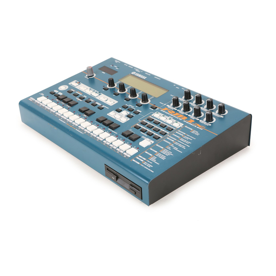
Page 5: Panel Layout
RM1x PANEL LAYOUT Front Panel 1. BPM Display 2. MIDI Data Monitors 3. LCD Display 4. Display Knobs 5. Function Buttons and Indicators 6. VOLUME Control 7. Real Time Controller Knobs & [KNOB] Button 8. Cursor Buttons 9. [NO -1] and [YES +1] Buttons 10. - Page 6 RM1x Rear Panel 1. STANDBY/ON Switch 2. DC IN Jack 3. CONTRAST Control 4. MIDI IN & OUT Connectors 5. L/MONO & R OUTPUT Jacks 6. PHONES Jack 7. FOOT SW Jack...
- Page 7 RM1x CIRCUIT BOARD LAYOUT...
-
Page 8: Disassembly Procedure
RM1x DISASSEMBLY PROCEDURE Bottom Case Assembly Remove the eight (8) screws marked [280] and the four (4) screws marked [281]. The bottom case assembly can then be removed. (Fig. 1) Rear View Bottom view (Fig.1) (Fig.2) [280]: Bind Head Tapping Screw-B 3.0X6 MFZN2BL (EP600230) [230]: Bind Head Tapping Screw-B 3.0X6 MFZN2BL (EP600230) - Page 9 RM1x Rear View Bottom view (Fig.3) [210]: Bind Head Tapping Screw-B 3.0X6 MFZN2BL (EP600230) [211]: Bind Head Tapping Screw-B 3.0X8 MFZN2BL (EP600190) [212]: Bonding Head Screw-B 3.0X10 MFZN2BL (VQ498000) PN Circuit Board Remove the bottom case assembly. (See Proce- dure 1.) Remove the DM circuit board.
- Page 10 RM1x Bottom View (Fig.6) [40]: Bind Head Tapping Screw-B 3.0X8 MFZN2BL (EP600190) [80]: Bind Head Tapping Screw-B 3.0X6 MFZN2BL (EP600230) [100]: Bind Head Tapping Screw-B 3.0X6 MFZN2BL (EP600230) Knob Circuit board Remove the bottom case assembly. (See Proce- dure 1.) Remove the DM circuit board.
- Page 11 RM1x HG73C205FD (XU947A00) SWX000 TONE GENERATOR NAME FUNCTION NAME FUNCTION Initial clear CMA3 Program address bus RFCLKI PLL Clock CMA8 Program address bus PLL Control CMA2 Program address bus AVDD_PLL Power supply read signal AVSS_PLL Ground CMA1 Program address bus...
- Page 12 RM1x HG73C201FD (XT890A00) SWX00 TONE GENERATOR NAME FUNCTION NAME FUNCTION Initial clear CMA3 RFCLKI PLL Clock CMA8 PLL Control CMA2 AVDD_PLL Power supply read signal AVSS_PLL Ground CMA1 Program address bus MODE0 Mode set high byte effective signal VCC7 Power supply...
- Page 13 RM1x SH7014 (XT437A00) CPU NAME FUNCTION NAME FUNCTION PE14 Port E PE15 Data bus Port E Ground Ground Data bus Power supply Address bus Data bus Ground XTAL Mode control EXTAL Mode control Non-maskable interrupt request Power supply Power supply...
- Page 14 RM1x HD63266F (XI939A00) FDC (Floppy Disk Controller) NAME FUNCTION NAME FUNCTION 8"//5" Data transmission speed /TRKO Track 00 signal XTALSET Clock select /INDEX Index signal /RESET Rest /RDATA Read data input from FDD E//RD Enable/Read XTAL2 RW//WR Read/write/Write EXTAL2 Clock...
- Page 15 RM1x SED1335F0B (XQ595A00) LCDC (LCD Controller) NAME FUNCTION NAME FUNCTION Data bus output for 4 bit dot VRAM address bus XECL S driver enable, chain clock XSCL Data bus shift clock Ground /VWR VRAM read/write X driver latch pulse /VCE...
- Page 16 RM1x...
- Page 17 RM1x 28CA1-8812706...
- Page 18 RM1x • DM Circuit Board MIDI-OUT MIDI-IN CONTRAST FOOT SW OUTLET/R OUTLET/L-MONO PHONES DC IN STAND BY/ON to LCD to PN-CN4 to PN-CN5 Component side DM:2NA-V260480...
- Page 19 RM1x • DM Circuit Board Patternside...
- Page 20 RM1x • PN 1/3Circuit Board Note: See parts list for details of circuit board component parts. See PANEL SWITCH TABLE on C2 of OVERALL CIRCUIT DIAGRAM. to DM-CN5 to DM-CM3 to DM-CN1 Component side to DM-CN4...
- Page 21 RM1x • PN 1/3Circuit Board Patternside PN: 2NA-V260490...
- Page 22 RM1x • PN 2/3 Circuit Board • PN 3/3 Circuit Board GATE TIME TIME STRECH CLOCK SHIFT VEROCITY VOLUME to DM-CN8 Component side PITCH BEND CUT OFF RESONANCE EG DECAY Component side Patternside Patternside Note: See parts list for details of circuit board component parts.
- Page 23 RM1x TEST PROGRAM & INITIALIZE 1.TEST PROGRAM PREPARATIONS Measuring instruments: low frequency oscillator, frequency counter, oscilloscope, volt meter (JIS- C curve), keyboard amplifier, etc. Jigs: MIDI cable, floppy disk (2HD, form atted), etc. TEST PROGRAM TEST No. TEST TEST RESULT...
- Page 24 When the auto mode test is entered, the following display will appear: Auto Mode ----------> error processing state Manual Mode -------> test number waiting state **RM1x TEST** AUTO However, this method does not correspond at MAIN Ver #.## the test of “ C-5 PANEL SWITCH ” .
- Page 25 RM1x Test End C-3 LCD ALL ON / OFF TEST After displaying the test result and the test will be finished. 03: LCD Check All the RAM data will be restored. Press the [F4] switch to exit the test, press the...
- Page 26 RM1x When it is normal, a piano tone is generated C-5 PANEL SWITCH TEST while being press on the switch. 05: Panel Switch NG is displayed when another switch is pressed and a piano tone does not generate. After this, the test advances to the next switch test when a correct switch is pressed.
- Page 27 RM1x Display Of Test Results C-10 KNOB 1 (BEAT STRETCH) TEST 05: Panel Switch 10: Knob 1 Push [MODE ] xxx 64 Test End (where xxx= current KNOB 1 value) After displaying the test result when the check to the [TAP] switch end and the test will be According to the target value displayed on the finished.
- Page 28 RM1x Display Of Test Results Display Of Test Results 18: FOOT SW 20: MIDI (IN/OUT) Not appearing 20: MIDI (IN/OUT) Test End After displaying the test result the test will be finished. TIME OUT After pressing the [F4] to exit the test, press the...
- Page 29 RM1x L ) : 1 kHz +/- 3.0 Hz, Sine wave OUTPUT ( C-24. FACTORY SETTINGS +2 +/- 2 dBm (10 kHz load), Distortion : less than 0.5% 24: Factory Set R ) : less than -76 dBm OUTPUT (...
- Page 30 RM1x Keyboard Velocity setting = 100 2. INITIARIZE Event Chase = If you wish to reset the RM1x’s settings to the factory condition, Setup Mode = Pattern Mode you can perform the Initialization operation. Song Number = Rec. track =...
- Page 31 Factory Set After the power is switched ON, a system diagnosis is run on the RM1x’s system. If the diagnosis finds the RAM to be defective, this message will appear and the memory will be reset to its original factory settings.
- Page 32 This will appear when you attempt to load a defective file. Illegal Format This will appear if the floppy disk is of a format which the RM1x is not able to handle. Check the contents of the disk. Disk Changed This will appear if you have exchanged disks when you should not have.
- Page 33 YAMAHA [ Music Sequencer --- voice part Date:08-SEP-1998 Model RMlx MIDI Implementation Chart Version : 1.0 Transmitted Recognized Remarks Function ... Basic Default 1 - 16 1 - 16 Memorized Channel Changed 1 - 16 1 - 16 Default Memorized...
- Page 34 YAMAHA [ Music Sequencer --- sequencer part Date:08-SEP-1998 Model RMlx MIDI Implementation Chart Version : 1.0 Transmitted Recognized Remarks Function ... Basic Default 1 - 16 1 - 16 Memorized Channel Changed Default Mode Messages Altered ************** Note 0 - 127...
-
Page 35: Midi Data Format
RM1x MIDI DATA FORMAT (3) TRANSMIT/RECEIVE DATA The RM1x tone generator and sequencer blocks handle different MIDIevents. These are listed seqparately in (3-1) CHANNEL VOICE MESSAGES the MIDI Data Format as well as in the MIDI Implementation Chart. (3-1-1) NOTE OFF... - Page 36 (3-2-3) ALL NOTE OFF (CONTROL NUMBER = 7BH , DATA VALUE = 0) F0H 7EH 0nH 06H 01H F7H ("n" is the device number, but the RM1x receives this in Turns off all notes of the corresponding channel which are on. However if Sustain or Sostenuto are on, Omni.)
- Page 37 IN | |----- NOTE OFF (3-3) SYSTEM COMMON MESSAGE |----- NOTE ON/OFF These are transmitted and received as Control Messages for RM1x functions. |----- KEY'S AFTER T OUCH They are not recorded as SEQUENCE DATA. |----- CONTROL CHANGE |----- PROGRAM CHANGE...
- Page 38 0cmmmmmm 11110111 End of Exclusive 0kssssss 0gifffff ss=08H-0FH, dd=on is received, and the PATTERN will be changed to the RM1x's sections A - P 0bbbbbbb respectively. 11110111 End of Exclusive Transmitted when you move between measures in the SONG mode.
- Page 39 RM1x 02 01 10 00..7F Reverb Parameter 11 Refer to Ef. Parameter List depends on Reverb type 00..7F Reverb Parameter 12 Refer to Ef. Parameter List depends on Reverb type 00..7F Reverb Parameter 13 Refer to Ef. Parameter List depends on Reverb type 00..7F...
- Page 40 RM1x nn 04 Not Used nn 05 00..01 Mono/Poly Mode 0:mono,1:poly nn 06 00..02 Same Note Number 0:single Key On Assign 1:multi 2:inst (for DRUM) nn 07 Not Used nn 08 28..58 Note Shift -24..+24[semitones] nn 09 00..FF Detune -12.8..+12.7[Hz]...
- Page 41 RM1x nn 6D Not Used nn 6E Not Used TOTAL SIZE 3F nn = PartNumber For the Drum Part, the following parameters have no effect. ¥Bank Select LSB ¥Portamento ¥Soft Pedal ¥Mono/Poly ¥Scale Tuning ¥Pitch EG <Table 1-6> Effect Type List...
-
Page 42: Parts List
RM1x PARTS LIST CONTENTS OVERALL ASSEMBLY ......... 2 LCD ASSEMBLY ..........4 PN-SW ASSEMBLY ..........5 ELECTRICAL PARTS ..........6 Note) DESTINATION ABBREVIATIONS J : Japanese model A: Australian model U: U.S. model E: European model C: Canadian model D: German model... - Page 43 RM1x OVERALL ASSEMBLY...
- Page 44 RM1x DESCRIPTION REMARKS PART NO. QTY RANK REF NO OVERALL ASSEMBLY RM1X Overall Assembly J,U,E (V273750) V2645400 Top Cover V2875900 LED Cover V2737900 LCD Assembly EP600190 Bind Head Tapping Screw-B 3.0X8 MFZN2BL PN-SW Assembly (V273800) EP600230 Bind Head Tapping Screw-B 3.0X6 MFZN2BL...
- Page 45 RM1x LCD ASSEMBLY PART NO. DESCRIPTION REMARKS REF NO QTY RANK RM1x LCD ASSEMBLY V2737900 LCD Assembly V2737600 LCD Cover VT282300 EDMMR03Y00 VB390800 Connector Base Post PH-12P TE Back-lit Assembly VT210200 YAK-08A-72 VT210100 VT287000 Connector Assembly B-LIGHT V2645700 Escutcheon V3203300...
- Page 46 RM1x PN-SW ASSEMBLY PN-SW Ass' y x 15 x 17 x 10 PART NO. DESCRIPTION REMARKS REF NO QTY RANK PN-SW ASSEMBLY RM1x PN-SW Assembly (V273800) NX820310 Circuit Board (V260500) Circuit Board NX820320 (V260510) Circuit Board NX820330 KNOB (V260520) V2689300...
- Page 47 RM1x DESCRIPTION REMARKS PART NO. QTY RANK REF NO ELECTRICAL PARTS RM1x NX820310 Circuit Board (XU710B0) V2604800 Circuit Board (XU709B0) NX820320 Circuit Board (XU710B0) NX820330 Circuit Board KNOB (XU710B0) V2604800 Circuit Board (XU709B0) Heat Sink T220M 25L (BA80852) EG330360 Bind Head Screw 3.0X6 MFZN2BL...
- Page 48 RM1x DESCRIPTION REMARKS PART NO. QTY RANK REF NO UB013100 Monolithic Ceramic Cap. B 1000P 50V K UB052100 Monolithic Ceramic Cap. SL 100P 50V J UB013150 Monolithic Ceramic Cap. C100 B 1500P 50V K UB052100 Monolithic Ceramic Cap. C101 SL 100P 50V J...
- Page 49 RM1x DESCRIPTION REMARKS PART NO. QTY RANK REF NO VT332900 Diode 1SS355 TE-17 VT332900 Diode 1SS355 TE-17 VQ282500 Diode MA737 VS201100 Diode D1F60 VZ016600 Diode D3FP3 VS201100 Diode D1F60 VT332900 Diode 1SS355 TE-17 XT437A00 SH7014 VK863100 IC Socket DICF-42CS-E VK863100...
- Page 50 RM1x DESCRIPTION REMARKS PART NO. QTY RANK REF NO Carbon Resistor (chip) RD255220 220.0 0.1 J Carbon Resistor (chip) RD256100 1.0K 0.1 J Carbon Resistor (chip) RD256100 1.0K 0.1 J Carbon Resistor (chip) RD257100 10.0K 0.1 J Carbon Resistor (chip) RD257100 10.0K 0.1 J...
- Page 51 RM1x PART NO. DESCRIPTION REMARKS REF NO QTY RANK RD154470 Carbon Resistor (chip) R137 47.0 1/4 J RD257470 Carbon Resistor (chip) R138 47.0K 0.1 J RD257120 Carbon Resistor (chip) R139 12.0K 0.1 J RD256470 Carbon Resistor (chip) R140 4.7K 0.1 J...
- Page 52 RM1x DESCRIPTION REMARKS PART NO. QTY RANK REF NO VR101400 Encoder EC16B24204 L=15 VZ085500 Tact Switch SKQNAM004A VZ085500 Tact Switch SKQNAM004A VS180900 Push Switch SKEYAG VS180900 Push Switch SKEYAG VZ085500 Tact Switch SKQNAM004A OCT DOWN VZ085500 Tact Switch SKQNAM004A OCT UP...
- Page 53 RM1x 28CC1-8812705 Note: See parts list for details of circuit board component parts.
- Page 54 RM1x KNOB: 28CC1-8812707(2/3) MVR: 28CC1-8812707(2/3) 28CC1-8812707(1/3) Note: See parts list for details of circuit board component parts.