Yamaha MG16/6FX Service Manual
Mixing console
Hide thumbs
Also See for MG16/6FX:
- Service manual (92 pages) ,
- Owner's manual (32 pages) ,
- Owner's manual (4 pages)
Advertisement
A manufacture number should use this
manual with goods of 9 or more figures.
The example of a manufacture number.
JCLJ01001
UCCLJ01001
CHNCL01001
9-11 figures
The service manual of PA 011678 should
be used for the goods whose manufacture
number is 7 figures.
PA 011678
The example of a manufacture number.
LK01001
011781
PA
200306-49800
MIXING CONSOLE
SERVICE MANUAL
I CONTENTS
SPECIFICATIONS
DIMENSIONS
PANEL LAYOUT
CIRCUIT BOARD LAYOUT & WIRING
DISASSEMBLY PROCEDURE
LSI PIN DESCRIPTION
IC BLOCK DIAGRAM
CIRCUIT BOARDS
INSPECTIONS
....................................................... 30/36
PARTS LIST
BLOCK DIAGRAM & LEVEL DIAGRAM
OVERALL CIRCUIT DIAGRAM
Copyright (c) Yamaha Corporation. All rights reserved. PDF-K338
............................................... 3/5
........................................................... 7
...................................... 8
.............................................. 12
............................. 14
.............................. 19
.................................. 21
........................................ 22
HAMAMATSU, JAPAN
'05.08
Advertisement
Table of Contents

Related Manuals for Yamaha MG16/6FX


Summary of Contents for Yamaha MG16/6FX
-
Page 1: Mixing Console
IC BLOCK DIAGRAM ........21 CIRCUIT BOARDS ........22 The example of a manufacture number. INSPECTIONS ............30/36 PARTS LIST LK01001 BLOCK DIAGRAM & LEVEL DIAGRAM OVERALL CIRCUIT DIAGRAM 011781 HAMAMATSU, JAPAN 200306-49800 Copyright (c) Yamaha Corporation. All rights reserved. PDF-K338 ’05.08... - Page 2 IMPOR TANT NOTICE This manual has been provided for the use of authorized Yamaha Retailers and their ser vice personnel. It has been assumed that basic service procedures inherent to the industry, and more specifically Yamaha Products, are already known and under- stood by the users, and have therefore not been restated.
-
Page 3: Specifications
MG16/6FX SPECIFICATIONS General Specifications 20 Hz-20 kHz +1 dB, -3 dB @+4 dBu, 600 Ω (with gain control at maximum level) Frequency Characteristics (ST OUT) 0.1% (THD+N) @+14 dBu, 20 Hz-20 kHz, 600 Ω (with gain control at maximum level) - Page 4 MG16/6FX Input Specifications Input Appropriate Max. Before Connector Input Connector Gain Sensitivity* Rated Level Impedance Impedance Clipping Specifications -80 dBu -60 dBu -40 dBu MIC INPUT (0.078 mV) (0.775 mV) (7.75 mV) 50-600 Ω mic 3 kΩ XLR-3-31 type (balanced)
- Page 5 MG16/6FX – –...
- Page 6 MG16/6FX MIC INPUT –80 dBu –60 dBu –40 dBu –60 (CH1 0.078 mV 0.775 mV 7.75 mV XLR-3-31 –36 dBu –16 dBu +4 dBu –16 12.3 mV 123 mV 1.23 V LINE INPUT –54 dBu –34 dBu –14 dBu 10 k –34...
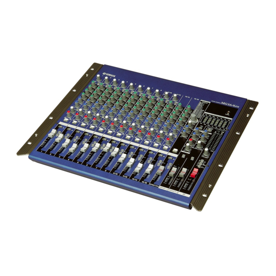
- Page 7 MG16/6FX DIMENSIONS H 108 101.3 W 423 Units: mm...
- Page 8 MG16/6FX PANEL LAYOUT Channel Control Section Channels Channels Channels 1 to 8 9/10 and 11/12 13/14 and 15/16 (Monaural) (Stereo) (Stereo) [GAIN] Control [PEAK] Indicator ] Switch (High Pass Filter) Equalizer ([HIGH], [MID], [LOW]) [AUX1] and [AUX2] Controls [PRE] Switch...
- Page 9 MG16/6FX Master Control Section [ST] Master Fader [GROUP] Faders (1-2, 3-4) [TO ST] Switch Master SEND ([AUX1], [AUX2], and [EFFECT] controls) RETURN ([AUX1], [AUX2], and [ST] Controls) [2TR IN] Control [PHANTOM +48 V] Switch Level-Meter Signal Switches [C-R/PHONES] Control Level Meter...
- Page 10 MG16/6FX Rear Input/Output Section Channel Input Jacks [INSERT I/O] Jacks Channel Input Jacks [GROUP OUT] (1 to 4) Jacks [ST OUT] (L, R) Jacks [C-R OUT] Jacks [SEND] Jacks [RETURN] L (MONO), R Jacks [REC OUT] (L, R) Jacks [2TR IN] Jacks...
- Page 11 MG16/6FX Connector Polarities INPUT OUTPUT Pin 1: Ground MIC INPUT, ST OUT Pin 2: Hot (+) Pin 3: Cold (–) LINE INPUT (monaural channels), Tip: Hot (+) GROUP OUT, ST OUT, C-R OUT, Ring: Cold (–) AUX1, AUX2, EFFECT* Sleeve: Ground...
-
Page 12: Main
MG16/6FX CIRCUIT BOARD LAYOUT & WIRING JACK JACK JACK MAIN Power switch and AC connector wiring WA595400 Brown Black Shrink tube (7 Places) WE735800... - Page 13 MG16/6FX MAIN circuit board and JACK circuit board wiring JACK 1/2 circuit board WD361600 WC712200 WE573200 CNE02 MAIN circuit board MAIN circuit board CNJ01 CNL02 Phones WE521800 WE521800 Jumper Wire (JACK 2/2 circuit board) WC703300 (9 places) CN102 (JACK 1/2 circuit board) --- CN101 (MAIN circuit board)
-
Page 14: Disassembly Procedure
MG16/6FX DISASSEMBLY PROCEDURE Rack Mount Angle (Time required: About 1 minute) Remove the two (2) screws marked [570A]. The rack mount angle R can then be removed. (Fig. 1) Remove the two (2) screws marked [570B]. The rack mount angle L can then be removed. (Fig. 1) - Page 15 MG16/6FX [A]: Bind Head T apping Screw-B 3.0X8 MFZN2W3 (WE774300) Photo.2 [530] [540] [530] [530]:Bind Head Tapping Screw-B 3.0X8 MFZN2W3 (WE774300) [540]:Bind Head Tapping Screw-S 3.0X6 MFZN2W3 (WE877900) IC02 IC03 Photo.1 [B]: Bind Head Tapping Screw-B 3.0X8 MFZN2W3 (WE774300) Photo.3 PS Circuit Board (Time required: About 4 minutes) Remove the bottom cover.
- Page 16 MG16/6FX [470A] [470B] [480A] [480B] [470A] [470B] [480B] [480A] [470A] [470B] [470]: Bind Head Tapping Screw-S [470]: Bind Head Tapping Screw-S 3.0X6 MFZN2W3 (WE877900) 3.0X6 MFZN2W3 (WE877900) [480]: Hex. Socket Set Screw [480]: Hex. Socket Set Screw 3.0X6 MFZN2B3 (WF419300) 3.0X6 MFZN2B3 (WF419300)
- Page 17 MG16/6FX MAIN, JACK (1/2, 2/2) Circuit Boards (Time required: About 22 minutes) Remove the rack mount angle L and R. (See procedure 1.) Remove the bottom cover. (See procedure 2.) Remove the PS circuit board and Heat sink. (See procedure 3.) Remove the side cover L and R.
- Page 18 MG16/6FX 7-12 Remove the two (2) screws marked [430]. Twist the eight (8) hooks of the MIX1 support (upper) to become straight, and the support and two (2) spacer can be removed from the MAIN circuit board. (Fig. 2, Photo. 10) 7-13 Remove the screw marked [440].
-
Page 19: Lsi Pin Description
MG16/6FX LSI PIN DESCRIPTION ZFX-2 (XY297A00) CPU DSP: ICM01 NAME FUNCTION NAME FUNCTION AXLR2 Audio Data Transmitt Unit 2/3 Left and Right Channel Frame Frequency Signal Audio Data Receive Unit 1 Data Input External Memory and I/O Data Bus Audio Data Receive Unit 2 Data Input... - Page 20 MG16/6FX µ PD78082 (XZ312A00) MCU DSP: ICM03 NAME FUNCTION NAME FUNCTION P12/ANI2 Non-connection P13/ANI3 P14/ANI4 Port 3 Port 1 / A/D converter analog input P15/ANI5 P16/ANI6 P35/PCL Port 3 / Clock output P17/ANI7 P36/BUZ Port 3 / Buzzer output P72/ASCK//SCK2...
-
Page 21: Ic Block Diagram
MG16/6FX IC BLOCK DIAGRAM 74HCU04DT (XZ110A00) NJM2068M-D(TE2) (X3505A00) NJM4580ED (XT157A00) MAIN: IC101, 201, 301, 401, 501, 601, 701, MAIN: IC102, 103, 202, 302, 303, 402, 502, DSP: ICM05 801, 901, A01, F02, G02, J02, J03, 503, 602, 702, 703, 802, 902-906,... -
Page 22: Circuit Boards
MG16/6FX CIRCUIT BOARDS DSP Circuit Board (X6354A0) ............22 MAIN Circuit Board (X6344C0) ..........23/25 JACK 1/2 Circuit Board (X6255B0) .......... 27/28 JACK 2/2 Circuit Board (X6255B0) ..........28 PS Circuit Board (X6343B0) ............29 Note: See parts list for details of circuit board component parts. - Page 23 MG16/6FX MAIN Circuit Board to JACK1/2-CN302 to JACK1/2-CN702 to JACK1/2-CN102 to JACK1/2-CN502 GAIN PEAK PEAK PEAK PEAK PEAK PEAK PEAK PEAK PEAK HIGH HIGH HI MID AUX1 AUX2 EFFECT PAN/BAL Fader 9/10 Component side 2NA-WE52180...
- Page 24 MG16/6FX to JACK1/2-CNA02 to JACK1/2-CNF02 to PS-CN02 to JACK1/2-CN902 to JACK1/2-CND02 to JACK1/2-CNK02 to PS-CN03 to JACK2/2-CNL02 PEAK PEAK PEAK ST GRAPHIC EQUALIZER HIGH HIGH HIGH HIGH HIGH HI MID HI MID HI MID HI MID HI MID LO MID...
- Page 25 MG16/6FX MAIN Circuit Board to DSP-CNM01 Pattern side 2NA-WE52180...
- Page 26 MG16/6FX Pattern side 2NA-WE52180...
- Page 27 MG16/6FX JACK1/2 Circuit Board LINE INSERT I/O to MAIN-CN101 to MAIN-CN301 to MAIN-CN501 to MAIN-CN701 GROUP OUT ST OUT to MAIN-CN901 to MAIN-CND01 to MAIN-CNK01 to MAIN-CNA01 to MAIN-CNF01 Component side 2NA-WE57320...
- Page 28 MG16/6FX JACK1/2 Circuit Board Pattern side JACK2/2 Circuit Board to MAIN-CNL01 PHONES Component side Pattern side 2NA-WE57320...
- Page 29 MG16/6FX PS Circuit Board to Power Switch, AC connector to MAIN -CNJ01 to MAIN -CNE02 Component side Pattern side 2NA-WE61260...
- Page 30 MG16/6FX INSPECTIONS Measurement conditions 1-1. Environment Normal temperature (10 to 35C) Normal humidity (45 to 85%) 1-2. Power Source The voltage is within +/-10%. AC Adaptor (PA-30) shall be used. WE523900 (H,W:230V) or WE524200 (U,V:120V), WE523700 (B:230V), WE524100 (K:220V), WE523600 (A:240V),...
- Page 31 MG16/6FX • DIGITAL EFFECT PROGRAM select switch PARAMETER control AUX1,AUX2 level control MAX when taking measurement only/ MIN otherwise ON switch ON(LED shall light) when taking measurement only/ OFF otherwise PFL switch ON when taking measurement only/ OFF otherwise EFFECT RTN Fader MAX when taking measurement only/ MIN otherwise •...
- Page 32 MG16/6FX Table 2.6.2 [dBu] INSERT OUT INPUT INPUT level GAIN REC OUT L REC OUT R MIC 1-8 -20 +/-2 – – CH1 INSERT IN Unspecified – +2.2 +/-2 +2.2 +/-2 CH2-8 INSERT IN Unspecified – +2.2 +/-2 – Table 2.6.3 Input Terminal STEREO IN [dBu]...
- Page 33 MG16/6FX 2-9. Channel Equalizer Characteristics In the state checked in 2-2 above, check the output level obtained at GROUP 1 OUT in the case of CH INPUT and ST CH INPUT L and at GROUP 2 OUT in the case of ST CH INPUT R when LO, HI and MID of INPUT are moved respectively.
- Page 34 MG16/6FX 2-12. PEAK LED light-up level Each LED shall light-up within the range specified in the table 2.12.1 when a signal is fed to the MIC input. Table 2.12.1 [dBu] INPUT PEAK LED -43 +/-2 2-13. Meter LED lighting check PEAK LED lights up, when ST output level reaches +17.5 +/-2dBu.
- Page 35 MG16/6FX 2-18. PHANTOM Connect a 10kΩ load resistance between the pin 1 and 2 of the MIC and short-circuit between the pin 2 and 3. Turn on the PHANTOM switch(LED shall light) and the voltage between pin 1 and 2 shall be within +35 +/-3V.
- Page 36 MG16/6FX...
- Page 37 MG16/6FX INPUT AUX2 C-R OUT C-R OUT INPUT Gain ST L OUT ST R OUT GROUP1-4 AUX1 EFFECT level PRE OFF PRE ON +1 +/-2 *1 +1 +/-2 *1 +4 +/-2 -4 +/-2 +6 +/-2 -4 +/-2 +6 +/-2 0 +/-2...
- Page 38 MG16/6FX INSERT OUT INPUT INPUT level GAIN REC OUT L REC OUT R MIC 1-8 -20 +/-2 – – CH1 INSERT IN Unspecified – +2.2 +/-2 +2.2 +/-2 CH2-8 INSERT IN Unspecified – +2.2 +/-2 – INPUT AUX2 C-R OUT...
- Page 39 MG16/6FX Level control f control Applied frequency Variation width –– +12 +/-2 HIGH 10kHz –– -12 +/-2 +15 +/-2.5 5kHz -15 +/-2.5 +15 +/-2.5 250Hz -15 +/-2.5 –– +12 +/-2 100Hz –– -12 +/-2 Level control Applied frequency Variation width...
- Page 40 MG16/6FX INPUT PEAK LED -43 +/-2 Fader/VR ST OUT GROUP OUT AUX OUT EFFECT OUT C-R OUT -78.0 -80.0 -75.0 -75.0 -72.0 -100.0 -100.0 -100.0 -100.0 -87.0...
- Page 41 MG16/6FX OUTPUT PROGRAM select switch PARAMETER OUTPUT level ST L OUT ST R OUT +4.5 +/-5 GROUP1-4 9: VOCAL ECHO 1 MIN AUX1,2 C-R OUT L +0.5 +/-5 C-R OUT R 1: HALL 1 ST L OUT : *1 -9 +/-30...
-
Page 42: Parts List
MIXING CONSOLE PARTS LIST CONTENTS OVERALL ASSEMBLY ..........2 ELECTRICAL PARTS ........4-39 Notes : DESTINATION ABBREVIATIONS A : Australian model M : South African model B : British model O : Chinese model C : Canadian model Q : South-east Asia model D : German model T : Taiwan model E : European model... -
Page 43: Jack1/2
MG16/6FX OVERALL ASSEMBLY M9 Hexagon nut & Washer are Accessories of Phone Jack. M16 Hexagon nut & Washer are Accessories of Connector. JACK1/2 JACK2/2 • Accessories AC Adaptor (PA-30) OUTPUT : AC18V X 2 1.4A (2) GND (3) AC (1) AC... - Page 44 MG16/6FX PART NO. DESCRIPTION REMARKS REF NO. RANK OVERALL ASSEMBLY MG16/6FX (WE71560) WE521800 Circuit Board MAIN WE573200 Circuit Board JACK(1/2,2/2) WC703300 Jumper Wire SMV2J P=2 13-40 WE522400 Circuit Board WE675900 Circuit Board WE735800 Connector Assembly V 2 4 2 2 4 0 0...
- Page 45 MG16/6FX ELECTRICAL PARTS PART NO. DESCRIPTION REMARKS REF NO. RANK ELECTRICAL PARTS MG16/6FX WE675900 Circuit Board (WE67580)(X6354A0) WE573200 Circuit Board JACK(1/2,2/2) (X6255B0) WE521800 Circuit Board MAIN (X6344C0) WE522400 Circuit Board (WE61260)(X6343B0) WE675900 Circuit Board (WE67580)(X6354A0) CM01 UR847470 Electrolytic Cap. CM02 UR847470 Electrolytic Cap.
- Page 46 MG16/6FX PART NO. DESCRIPTION REMARKS REF NO. RANK RM07 RD358100 Carbon Resistor (chip) 100K 1/16W J RD358100 Carbon Resistor (chip) 100K 1/16W J RM11 RD356100 Carbon Resistor (chip) 1/16W J RM12 RD356100 Carbon Resistor (chip) 1/16W J RM13 HV753220 Flame Proof C.Resistor 2.2 1/4W J...
- Page 47 MG16/6FX PART NO. DESCRIPTION REMARKS REF NO. RANK C873 UR847100 Electrolytic Cap. C874 UR847100 Electrolytic Cap. C991 V J 0 9 7 4 0 0 Electrolytic Cap. C992 V J 0 9 7 4 0 0 Electrolytic Cap. C993 UR877100 Electrolytic Cap.
- Page 48 MG16/6FX PART NO. DESCRIPTION REMARKS REF NO. RANK JKL01 V 9 8 1 2 6 0 0 Phone Jack ST MSJ-064-20B B PHONES JKL02 V 9 8 1 2 6 0 0 Phone Jack ST MSJ-064-20B B C-R OUT L...
- Page 49 MG16/6FX PART NO. DESCRIPTION REMARKS REF NO. RANK R878 RF356470 Carbon Resistor (chip) 4.7K 1/16W D R991 HB026680 Metal Film Resistor 6.8K 1/4W F R992 HB026680 Metal Film Resistor 6.8K 1/4W F R993 RD354100 Carbon Resistor (chip) 1/16W J R994...
- Page 50 MG16/6FX PART NO. DESCRIPTION REMARKS REF NO. RANK C136 US062100 Ceramic Capacitor-SL(chip) 100P 50V J C137 US061680 Ceramic Capacitor-SL(chip) 68P 50V J C138 V 9 7 2 6 6 0 0 Electrolytic Cap. C139 US064100 Ceramic Capacitor-B(chip) 0.01 50V K...
- Page 51 MG16/6FX PART NO. DESCRIPTION REMARKS REF NO. RANK C327 V 9 7 2 6 6 0 0 Electrolytic Cap. C328 V 9 7 2 6 6 0 0 Electrolytic Cap. C329 US063100 Ceramic Capacitor-B(chip) 1000P 50V K C331 V 9 7 2 7 6 0 0 Electrolytic Cap.
- Page 52 MG16/6FX PART NO. DESCRIPTION REMARKS REF NO. RANK C521 US061330 Ceramic Capacitor-CH(chip) 33P 50V J C522 US062100 Ceramic Capacitor-SL(chip) 100P 50V J C523 UA653390 Mylar Capacitor 3900P 50V J C524 US062100 Ceramic Capacitor-SL(chip) 100P 50V J C525 US061470 Ceramic Capacitor-CH(chip)
- Page 53 MG16/6FX PART NO. DESCRIPTION REMARKS REF NO. RANK C715 US062100 Ceramic Capacitor-SL(chip) 100P 50V J C716 US064100 Ceramic Capacitor-B(chip) 0.01 50V K C717 V 9 7 2 6 5 0 0 Electrolytic Cap. C718 V 9 7 2 6 5 0 0 Electrolytic Cap.
- Page 54 MG16/6FX PART NO. DESCRIPTION REMARKS REF NO. RANK C909 US062470 Ceramic Capacitor-SL(chip) 470P 50V J C910 V 9 7 2 6 2 0 0 Electrolytic Cap. 470 6.3V C911 V 9 7 2 6 2 0 0 Electrolytic Cap. 470 6.3V...
- Page 55 MG16/6FX PART NO. DESCRIPTION REMARKS REF NO. RANK CA07 US062100 Ceramic Capacitor-SL(chip) 100P 50V J CA08 US062100 Ceramic Capacitor-SL(chip) 100P 50V J CA09 US062470 Ceramic Capacitor-SL(chip) 470P 50V J CA10 V 9 7 2 6 2 0 0 Electrolytic Cap.
- Page 56 MG16/6FX PART NO. DESCRIPTION REMARKS REF NO. RANK CB04 US062100 Ceramic Capacitor-SL(chip) 100P 50V J CB05 US062100 Ceramic Capacitor-SL(chip) 100P 50V J CB06 US064100 Ceramic Capacitor-B(chip) 0.01 50V K CB07 US064100 Ceramic Capacitor-B(chip) 0.01 50V K CB08 US062100 Ceramic Capacitor-SL(chip)
- Page 57 MG16/6FX PART NO. DESCRIPTION REMARKS REF NO. RANK CC17 UA654390 Mylar Capacitor 0.039 50V J CC18 UA654390 Mylar Capacitor 0.039 50V J CC19 US064100 Ceramic Capacitor-B(chip) 0.01 50V K CC20 UA652820 Mylar Capacitor 820P 50V J CC21 UA652820 Mylar Capacitor...
- Page 58 MG16/6FX PART NO. DESCRIPTION REMARKS REF NO. RANK CE09 US061680 Ceramic Capacitor-SL(chip) 68P 50V J CE10 V 9 7 2 6 6 0 0 Electrolytic Cap. CE11 V 9 7 2 6 6 0 0 Electrolytic Cap. CE12 US064100 Ceramic Capacitor-B(chip) 0.01 50V K...
- Page 59 MG16/6FX PART NO. DESCRIPTION REMARKS REF NO. RANK CK16 V 9 7 2 6 6 0 0 Electrolytic Cap. CK17 V 9 7 2 6 5 0 0 Electrolytic Cap. CK18 V 9 7 2 6 6 0 0 Electrolytic Cap.
- Page 60 MG16/6FX PART NO. DESCRIPTION REMARKS REF NO. RANK CL17 US062220 Ceramic Capacitor-SL(chip) 220P 50V CL18 US064100 Ceramic Capacitor-B(chip) 0.01 50V K CL19 US061220 Ceramic Capacitor-CH(chip) 22P 50V J CL20 US061220 Ceramic Capacitor-CH(chip) 22P 50V J CL21 V 9 7 2 6 6 0 0 Electrolytic Cap.
- Page 61 MG16/6FX PART NO. DESCRIPTION REMARKS REF NO. RANK IC702 X3505A00 NJM2068M-D(TE2) OP AMP IC703 X3505A00 NJM2068M-D(TE2) OP AMP IC801 XT157A00 NJM4580ED OP AMP IC802 X3505A00 NJM2068M-D(TE2) OP AMP IC901 XT157A00 NJM4580ED OP AMP IC902 X3505A00 NJM2068M-D(TE2) OP AMP -906 X3505A00...
- Page 62 MG16/6FX PART NO. DESCRIPTION REMARKS REF NO. RANK LDC01 V 9 8 5 4 5 0 0 LED Yellow HFY803037P-50-0 ST 15/16 LDC02 V 9 8 5 4 5 0 0 LED Yellow HFY803037P-50-0 PFL 15/16 LDE01 V 9 8 5 4 5 0 0...
- Page 63 MG16/6FX PART NO. DESCRIPTION REMARKS REF NO. RANK Q407 VV556400 Transistor 2SC2412K Q,R,S Q407 WC529400 Transistor KTC3875S-Y,GR-RTK/ Q408 VV556500 Transistor 2SA1037AK Q,R,S Q408 WC529500 Transistor KTA1504S-Y,GR-RTK/ Q409 VV556400 Transistor 2SC2412K Q,R,S Q409 WC529400 Transistor KTC3875S-Y,GR-RTK/ Q501 V 7 4 2 1 7 0 0...
- Page 64 MG16/6FX PART NO. DESCRIPTION REMARKS REF NO. RANK QA06 VV556500 Transistor 2SA1037AK Q,R,S QA06 WC529500 Transistor KTA1504S-Y,GR-RTK/ QE01 VV556400 Transistor 2SC2412K Q,R,S QE01 WC529400 Transistor KTC3875S-Y,GR-RTK/ QE02 VV556500 Transistor 2SA1037AK Q,R,S QE02 WC529500 Transistor KTA1504S-Y,GR-RTK/ QE03 VV556400 Transistor 2SC2412K Q,R,S...
- Page 65 MG16/6FX PART NO. DESCRIPTION REMARKS REF NO. RANK R204 RF357470 Carbon Resistor (chip) 47K 1/16W D R205 RD354100 Carbon Resistor (chip) 1/16W J R206 RF356220 Carbon Resistor (chip) 2.2K 1/16W D R207 RF356390 Carbon Resistor (chip) 3.9K 1/16W D R208...
- Page 66 MG16/6FX PART NO. DESCRIPTION REMARKS REF NO. RANK R326 RD356560 Carbon Resistor (chip) 5.6K 1/16W J R327 RD356820 Carbon Resistor (chip) 8.2K 1/16W J R328 RD356470 Carbon Resistor (chip) 4.7K 1/16W J R329 RD356820 Carbon Resistor (chip) 8.2K 1/16W J...
- Page 67 MG16/6FX PART NO. DESCRIPTION REMARKS REF NO. RANK R457 RD355220 Carbon Resistor (chip) 220 1/16W J R458 RD357120 Carbon Resistor (chip) 12K 1/16W J R459 RD356150 Carbon Resistor (chip) 1.5K 1/16W J R460 HF455100 Carbon Resistor 100 1/4W J R461...
- Page 68 MG16/6FX PART NO. DESCRIPTION REMARKS REF NO. RANK R614 RF357330 Carbon Resistor (chip) 33K 1/16W D R615 RF357330 Carbon Resistor (chip) 33K 1/16W D R616 RD358220 Carbon Resistor (chip) 220K 1/16W J R617 RD357160 Carbon Resistor (chip) 16K 1/16W J...
- Page 69 MG16/6FX PART NO. DESCRIPTION REMARKS REF NO. RANK R738 RD356470 Carbon Resistor (chip) 4.7K 1/16W J R739 HF456330 Carbon Resistor 3.3K 1/4W J R740 RD358100 Carbon Resistor (chip) 100K 1/16W J R741 RD357360 Carbon Resistor (chip) 36K 1/16W J R742...
- Page 70 MG16/6FX PART NO. DESCRIPTION REMARKS REF NO. RANK R902 RF356220 Carbon Resistor (chip) 2.2K 1/16W D R903 RF356390 Carbon Resistor (chip) 3.9K 1/16W D R904 RD357180 Carbon Resistor (chip) 18K 1/16W J R905 RD357100 Carbon Resistor (chip) 10K 1/16W J...
- Page 71 MG16/6FX PART NO. DESCRIPTION REMARKS REF NO. RANK -980 RD356470 Carbon Resistor (chip) 4.7K 1/16W J R981 RD357220 Carbon Resistor (chip) 22K 1/16W J R982 RD357220 Carbon Resistor (chip) 22K 1/16W J R983 RD357180 Carbon Resistor (chip) 18K 1/16W J...
- Page 72 MG16/6FX PART NO. DESCRIPTION REMARKS REF NO. RANK RA68 RD355220 Carbon Resistor (chip) 220 1/16W J RA69 RD356680 Carbon Resistor (chip) 6.8K 1/16W J RA70 RD356680 Carbon Resistor (chip) 6.8K 1/16W J RA71 RD357150 Carbon Resistor (chip) 15K 1/16W J...
- Page 73 MG16/6FX PART NO. DESCRIPTION REMARKS REF NO. RANK RC06 RD355220 Carbon Resistor (chip) 220 1/16W J RC07 RD356220 Carbon Resistor (chip) 2.2K 1/16W J RC08 RD356220 Carbon Resistor (chip) 2.2K 1/16W J RC09 RD357200 Carbon Resistor (chip) 20K 1/16W J...
- Page 74 MG16/6FX PART NO. DESCRIPTION REMARKS REF NO. RANK RE10 RD357220 Carbon Resistor (chip) 22K 1/16W J RE11 RD357120 Carbon Resistor (chip) 12K 1/16W J RE12 RD356150 Carbon Resistor (chip) 1.5K 1/16W J RE13 RD357180 Carbon Resistor (chip) 18K 1/16W J...
- Page 75 MG16/6FX PART NO. DESCRIPTION REMARKS REF NO. RANK RD356470 Carbon Resistor (chip) 4.7K 1/16W J RJ16 RD357100 Carbon Resistor (chip) 10K 1/16W J RD357100 Carbon Resistor (chip) 10K 1/16W J RJ19 RD358100 Carbon Resistor (chip) 100K 1/16W J RD358100 Carbon Resistor (chip)
- Page 76 MG16/6FX PART NO. DESCRIPTION REMARKS REF NO. QTY RANK RL19 RD357180 Carbon Resistor (chip) 18K 1/16W J RL20 RD356470 Carbon Resistor (chip) 4.7K 1/16W J RL21 HF456150 Carbon Resistor 1.5K 1/4W J HF456150 Carbon Resistor 1.5K 1/4W J RL25 RD357220...
- Page 77 MG16/6FX PART NO. DESCRIPTION REMARKS REF NO. RANK SW601 V 9 6 8 3 6 0 0 Push Switch PS-22E85L52 HPF 6 SW602 V 9 6 8 3 6 0 0 Push Switch PS-22E85L52 PFL 6 SW603 V 9 6 8 3 6 0 0...
- Page 78 MG16/6FX PART NO. DESCRIPTION REMARKS REF NO. RANK VR301 V 9 7 9 0 5 0 0 Rotary Variable Resistor RD 10K XV09213Y GAIN 3 VR302 V 8 2 6 4 7 0 0 Rotary Variable Resistor B 50K XV09213P...
- Page 79 MG16/6FX PART NO. DESCRIPTION REMARKS REF NO. RANK VRA01 V 9 7 9 1 1 0 0 Rotary Variable Resistor C 20K XV012313 GAIN 11/12 VRA02 V 9 7 9 1 2 0 0 Rotary Variable Resistor XV012313YGPV 1B50K LOW 11/12...
- Page 80 MG16/6FX PART NO. DESCRIPTION REMARKS REF NO. RANK UR838100 Electrolytic Cap. 100 16V VF611200 Monolithic Ceramic Cap. 0.1 50V Z VF611200 Monolithic Ceramic Cap. 0.1 50V Z UR847100 Electrolytic Cap. UR877470 Electrolytic Cap. UR858470 Electrolytic Cap. 470 35V WD399600 Electrolytic Cap.
-
Page 81: Circuit Diagram
MIXING CONSOLE MG16/6FX CIRCUIT DIAGRAM CONTENTS BLOCK DIAGRAM ....3 OVERALL CIRCUIT DIAGRAM MAIN ................4-10 JACK 1/2 ..............11, 12 JACK 2/2 ................. 8 DSP ................13 PS ................... 14 Notation for Circuit Diagrams 1. How to identify inter-sheet connectors... -
Page 82: Jack2/2
BLOCK DIAGRAM & LEVEL DIAGRAM MG16/6FX JACK1/2 JK101, 201, 301, CH IN MAIN +48V 401, 501, 601, CH1-8 701, 801 PHANTOM GROUP OUT [-60dBu to -16dBu] IC101, 201, 301, 401, IC103, 303, IC102, 202, 302, 402, ICF01a (8P) ICF02b (8P) - Page 83 OVERALL CIRCUIT DIAGRAM 1/11 (MAIN) MG16/6FX MAIN OP AMP to Page 8: P2 to Page 6: P9 OP AMP to Page 8: P3 OP AMP OP AMP to Page 9: K8 OP AMP to Page 9: J8 to Page 9: H8...
- Page 84 OVERALL CIRCUIT DIAGRAM 2/11 (MAIN) MG16/6FX OP AMP MAIN to Page 8: P2 OP AMP to Page 8: P3 OP AMP OP AMP to Page 9: K8 OP AMP to Page 9: J8 to Page 9: H8 to Page 9: G8...
- Page 85 OVERALL CIRCUIT DIAGRAM 3/11 (MAIN) MG16/6FX MAIN to Page 8: P2 OP AMP to Page 8: P3 OP AMP OP AMP OP AMP to Page 9: K8 OP AMP to Page 9: J8 CH9/10 OP AMP to Page 9: H8...
- Page 86 OVERALL CIRCUIT DIAGRAM 4/11 (MAIN) MG16/6FX from Page 6: C11 from Page 6: B11 MAIN OP AMP OP AMP to Page 8: P2 CH13/14 to Page 8: P3 OP AMP OP AMP OP AMP to Page 9: K8 OP AMP...
- Page 87 OVERALL CIRCUIT DIAGRAM 5/11 (MAIN, JACK2/2) MG16/6FX MAIN OP AMP OP AMP from Page 4: A1, Page 5: A1 OP AMP Page 6: A1, Page 7: A1 to JACK1/2 Page 9: F8, Page 10: A1 -CNK02 OP AMP (to Page 12: D2)
- Page 88 OVERALL CIRCUIT DIAGRAM 6/11 (MAIN) MG16/6FX to JACK1/2-CNF02 (to Page 12: D5) to PS-CN02 (to Page 14: A3) MAIN to Page 8: P7 to Page 8: P7 to Page 8: P7 to Page 8: P8 OP AMP OP AMP OP AMP...
- Page 89 OVERALL CIRCUIT DIAGRAM 7/11 (MAIN) MG16/6FX to Page 8: P2 MAIN from Page 7: C11 to Page 8: P3 OP AMP to Page 9: K8 to Page 9: J8 to PS-CN03 (to Page 14: A4) OP AMP to Page 9: H8...
- Page 90 OVERALL CIRCUIT DIAGRAM 8/11 (JACK1/2) MG16/6FX to MAIN-CN501 to MAIN-CN701 (to Page 5: P3) (to Page 5: P8) from Page 12: K2 JACK1/2 CH 5 MIC 5 LINE 5 INSERT I/O 5 CH 6 MIC 6 LINE 6 INSERT I/O 6...
- Page 91 OVERALL CIRCUIT DIAGRAM 9/11 (JACK1/2) MG16/6FX to MAIN-CNK01 (to Page 8: A2) JACK1/2 to MAIN-CND01 13/L (to Page 7: P6) to Page 11: K2 ST OUT L CH13 (L)/CH14 (R) 14/R 13/L 14/R MIC 9/10 ST OUT R CH9 (L)/CH10 (R)
-
Page 92: Dsp
OVERALL CIRCUIT DIAGRAM 10/11 (DSP) MG16/6FX to MAIN-CNE01 (to Page 10: H4) INVERTER INVERTER INVERTER ZFX-2 OP AMP DRAM 4M OP AMP : Ceramic Capacitor : Mylar Capacitor : Flame Proof C. Resistor 28CC1-8834994... - Page 93 OVERALL CIRCUIT DIAGRAM 11/11 (PS) MG16/6FX REGULATOR +15V ON/STANDBY (POWER) REGULATOR -15V AC ADAPTOR REGULATOR +12V to MAIN-CNJ01 (to Page 9: A1) KIA7815API(X4930A00) KIA7915PI(X4931A00) REGULATOR +5V REGULATOR -15V REGULATOR +15V IC01 IC02 to MAIN-CNE02 (to Page 10: H2) 1: COMMON...