JVC KD-G311 Service Manual
Cd receiver
Hide thumbs
Also See for KD-G311:
- Instructions manual (115 pages) ,
- Installation & connection manual (2 pages) ,
- Service manual (79 pages)
Advertisement
Table of Contents
SERVICE MANUAL
4
2005
MA134
KD-G311,KD-G312,KD-G317
1
PRECAUTIONS . . . . . . . . . . . . . . . . . . . . . . . . . . . . . . . . . . . . . . . . . . . . . . . . . . . . . . . . . . . . . . . . . . . . . . . 1-3
2
SPECIFIC SERVICE INSTRUCTIONS . . . . . . . . . . . . . . . . . . . . . . . . . . . . . . . . . . . . . . . . . . . . . . . . . . . . . . 1-6
3
DISASSEMBLY . . . . . . . . . . . . . . . . . . . . . . . . . . . . . . . . . . . . . . . . . . . . . . . . . . . . . . . . . . . . . . . . . . . . . . . 1-7
4
ADJUSTMENT . . . . . . . . . . . . . . . . . . . . . . . . . . . . . . . . . . . . . . . . . . . . . . . . . . . . . . . . . . . . . . . . . . . . . . . 1-25
5
TROUBLESHOOTING . . . . . . . . . . . . . . . . . . . . . . . . . . . . . . . . . . . . . . . . . . . . . . . . . . . . . . . . . . . . . . . . . 1-26
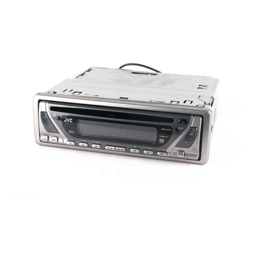
CD RECEIVER
KD-G311
STEERING CABLE
CONTROL PANEL
SILVER
TABLE OF CONTENTS
COPYRIGHT © 2005 Victor Company of Japan, Limited
KD-G311,KD-G312
KD-G317
KD-G312
KD-G317
BLACK
BLACK
KD-G311,KD-G312
Area suffix
E ------------ Southern Europe
EX ------------ Northern Europe
EY ------------- Eastern Europe
EU ------------------------- Turkey
KD-G317
Area suffix
EE -------- Russian Federation
No.MA134
2005/4
Advertisement
Table of Contents

Related Manuals for JVC KD-G311


Summary of Contents for JVC KD-G311
-
Page 1: Table Of Contents
SERVICE MANUAL CD RECEIVER MA134 2005 KD-G311,KD-G312,KD-G317 KD-G311,KD-G312 KD-G311,KD-G312 Area suffix E ------------ Southern Europe EX ------------ Northern Europe EY ------------- Eastern Europe EU ------------------------- Turkey KD-G317 KD-G317 Area suffix EE -------- Russian Federation KD-G311 KD-G312 KD-G317 STEERING CABLE CONTROL PANEL... - Page 2 Signal-to-Noise Ratio 70 dB Line-Out Level/Impedance 2.5 V/20 kΩ load (full scale) Output Impedance 1 kΩ Other Terminal Steering wheel remote input (KD-G311,KD-G312) TUNER SECTION Frequency Range 87.5 MHz to 108.0 MHz FM1/FM2 (KD-G317) 87.5 MHz to 108.0 MHz FM3 (KD-G317) 65.00 MHz to 74.00 MHz...
-
Page 3: Precautions
SECTION 1 PRECAUTIONS Safety Precautions Burrs formed during molding may be left over on some parts of the chassis. Therefore, pay attention to such burrs in the case of preforming repair of this system. Please use enough caution not to see the beam directly or touch it in case of an adjustment or operation check. - Page 4 Preventing static electricity Electrostatic discharge (ESD), which occurs when static electricity stored in the body, fabric, etc. is discharged, can destroy the laser diode in the traverse unit (optical pickup). Take care to prevent this when performing repairs. 1.2.1 Grounding to prevent damage by static electricity Static electricity in the work area can destroy the optical pickup (laser diode) in devices such as CD players.
- Page 5 Important for laser products 5.CAUTION : If safety switches malfunction, the laser is able 1.CLASS 1 LASER PRODUCT to function. 2.DANGER : Invisible laser radiation when open and inter 6.CAUTION : Use of controls, adjustments or performance of lock failed or defeated. Avoid direct exposure to beam. procedures other than those specified here in may result in 3.CAUTION : There are no serviceable parts inside the hazardous radiation exposure.
-
Page 6: Specific Service Instructions
SECTION 2 SPECIFIC SERVICE INSTRUCTIONS HOW TO IDENTIFY MODELS 2.1.1 NAME PLATE (as same as KD-G312, KD-G317) Discernment sign 1-6 (No.MA134) -
Page 7: Disassembly
SECTION 3 DISASSEMBLY Main body section 3.1.1 Removing the front panel assembly (See Fig.1) (1) Push the detach button in the lower right part of the front panel assembly and remove the front panel assembly. Front panel assembly Detach button Fig.1 3.1.2 Removing the bottom cover (See Fig.2) - Page 8 3.1.5 Removing the rear bracket (See Fig.5) • Remove the bottom cover. (1) For KD-G311 and KD-G312, remove the four screws D, Rear bracket one screw E and two screws F attaching the rear bracket on the back side of the main body.
- Page 9 3.1.7 Removing the CD mechanism assembly (See Fig. 7) • Remove the front panel assembly, bottom cover, side panel, rear bracket and main board. Reference: Remove the front chassis assembly as required. (1) Remove the three screws H attaching the CD mechanism assembly on the top chassis.
- Page 10 CD Mechanism Assembly 3.2.1 Removing the top cover (See Figs.1 and 2) (1) Remove the two screws A on the both side of the body. (2) Lift the front side of the top cover and move the top cover backward to release the two joints a. Top cover Joints a Fig.1...
- Page 11 3.2.2 Removing the connector board Wires (See Figs.3 to 5) CAUTION: Before disconnecting the flexible wire from the pickup, solder the short-circuit point on the pickup. No observance of this in- struction may cause damage of the pickup. (1) Remove the screw B fixing the connector board. (2) Solder the short-circuit point on the connector board.
- Page 12 3.2.3 Removing the DET switch (See Figs.6 and 7) (1) Extend the two tabs c of the feed sw. holder and pull out the switch. (2) Unsolder the DET switch wire if necessary. DET switch Connector board Pickup Fig.6 Tab c DET switch DET switch wire Tab c...
- Page 13 3.2.4 Removing the chassis unit (See Figs.8 and 9) • Prior to performing the following procedure, remove the top Chassis unit cover and connector board. Suspension spring (L) Suspension spring (R) (1) Remove the two suspension springs (L) and (R) attaching the chassis unit to the frame.
- Page 14 3.2.5 Removing the clamper assembly (See Figs.10 and 11) • Prior to performing the following procedure, remove the top cover. (1) Remove the clamper arm spring. Clamper arm (2) Move the clamper assembly in the direction of the arrow to spring release the two joints d.
- Page 15 3.2.6 Removing the loading / feed motor assembly (See Figs.12 and 13) • Prior to performing the following procedure, remove the top cover, connector board and chassis unit. (1) Remove the screw C and move the loading / feed motor assembly in the direction of the arrow to remove it from the chassis rivet assembly.
- Page 16 3.2.7 Removing the pickup unit Pickup unit (See Figs.14 to 18) • Prior to performing the following procedure, remove the top cover, connector board and chassis unit. (1) Remove the screw D and pull out the pu. shaft holder from the pu.
- Page 17 3.2.9 Removing the trigger arm Joint k (See Figs.19 and 20) • Prior to performing the following procedure, remove the top cover, connector board and clamper unit. (1) Turn the trigger arm in the direction of the arrow to release Trigger arm the joint k and pull out upward.
- Page 18 3.2.11 Removing the mode sw. / select lock arm Link plate Joint t (See Figs.22 and 23) Mode sw. • Prior to performing the following procedure, remove the top plate assembly. Select lock arm (1) Bring up the mode sw. to release from the link plate (joint t) and turn in the direction of the arrow to release the joint u.
- Page 19 3.2.12 Reassembling the mode sw. / select lock arm Select lock arm spring (See Figs.24 to 26) REFERENCE: Hook w Reverse the above removing procedure. Joint v (1) Reattach the select lock arm spring to the top plate and set Joint v the shorter end of the select lock arm spring to the hook w on the top plate.
- Page 20 3.2.13 Removing the select arm R / link plate Link plate Joint r Joint c' (See Figs.27 and 28) Select arm R Joint b' • Prior to performing the following procedure, remove the top plate assembly. (1) Bring up the select arm R to release from the link plate (joint a') and turn as shown in the figure to release the two Joint b' joints b' and joint c'.
- Page 21 3.2.15 Removing the loading roller assembly (See Figs.31 to 33) Loading roller assembly • Prior to performing the following procedure, remove the Roller guide clamper assembly and top plate assembly. spring (1) Push inward the loading roller assembly on the gear side and detach it upward from the slot of the joint g' of the lock arm rivet assembly.
- Page 22 3.2.16 Removing the loading gear 5, 6 and 7 Loading gear bracket (See Figs.35 and 36) • Prior to performing the following procedure, remove the top Loading gear 6 cover, chassis unit, pickup unit and top plate assembly. (1) Remove the screw K attaching the loading gear bracket. The loading gear 6 and 7 come off the loading gear brack- (2) Pull out the loading gear 5.
- Page 23 3.2.17 Removing the gears Joint p' (See Figs.37 to 40) • Prior to performing the following procedure, remove the top Change plate cover, chassis unit, top plate assembly and pickup unit. rivet assembly • Pull out the loading gear 3. (See Fig.35.) (1) Pull out the feed gear.
- Page 24 3.2.18 Removing the turn table / spindle motor Turn table (See Figs.41 and 42) • Prior to performing the following procedure, remove the top cover, connector board, chassis unit and clamper assembly. (1) Remove the two screws L attaching the spindle motor as- sembly through the slot of the turn table on top of the body.
-
Page 25: Adjustment
(3) Digital tester Output Level Line out 2.5V (Vol. MAX) (4) Tracking offset meter (5) Test Disc JVC :CTS-1000 Dummy load (6) Extension cable for check Exclusive dummy load should be used for AM,and FM. For FM EXTSH002-22P × 1... -
Page 26: Troubleshooting
SECTION 5 TROUBLESHOOTING Feed section Is the voltage out put at Is the wiring for IC541 Is 5V present at IC501 Check CD8V. IC541 pin 40, 5V or 0V? pin 40 correct? pins 3,12 and 21? Check the vicinity of IC541. - Page 27 Signal processing section Compare the L-ch and Is the sound output from No sound from either R-ch to locate the both channels (L, R)? channel. defective point. Check the vicinity of the Normal Is 9V present at IC161 IC901 audio power pin 32? supply.
- Page 28 Maintenance of laser pickup Replacement of laser pickup (1) Cleaning the pick up lens Before you replace the pick up, please try to clean the lens Turn off the power switch and,disconnect the with a alcohol soaked cotton swab. power cord from the AC outlet. (2) Life of the laser diode When the life of the laser diode has expired, the following symptoms will appear.
- Page 29 16 PIN CORD DIAGRAM Black Green VI/BK Violet GY/BK Blue Gray BL/WH WH/BK White Yellow GN/BK Brown VI/BK GY/BK WH/BK GN/BK MEMORY MEMORY BACKUP DIRECT TO BATTERY +12Volt BL/WH REMOTE ACC + 12Volt GROUND Rear Right Auto Antenna Front Right Line Front Left...
- Page 30 Victor Company of Japan, Limited AV & MULTIMEDIA COMPANY CAR ELECTRONICS CATEGORY 10-1,1chome,Ohwatari-machi,Maebashi-city,371-8543,Japan (No.MA134) Printed in Japan...
- Page 31 BLACK Contents Block diagram (For KD-G311 and KD-G312) Standard schematic diagrams (For KD-G311 and KD-G312 E,EX,EY,EU version) Printed circuit boards (For KD-G311 and KD-G312 E,EX,EY,EU version) Standard schematic diagrams (For KD-G311 and KD-G312 E2,EX2,EY2,EU2 version) Printed circuit boards (For KD-G311 and KD-G312 E2,EX2,EY2,EU2 version)
-
Page 32: Safety Precaution
Safety precaution Burrs formed during molding may be left over on some parts of the chassis. Therefore, pay attention to such burrs in the case of preforming repair of this system. Please use enough caution not to see the beam directly or touch it in case of an adjustment or operation check. - Page 33 Block diagram (For KD-G311 and KD-G312) TU.L IC171 TU.R FM/AM OP AMP TUNER Main amplifier & CD servo control section FMVT VF1, VF2, VT1 AMVT VT2, LD, MD PICK UP FM/AM LM0, LM1 Q781, Q782 TRACKING+, BUS0 to 3 MUTE...
-
Page 34: Standard Schematic Diagrams
Standard schematic diagrams (For KD-G311 and KD-G312 E, EX, EY, EU version) Main amplifier section D243 R248 R244 C243 R243 0.047 180k R245 C241 1/50 R242 R241 IC301 C242 22/16 LA47516 Q241 QAU0313-001 2SD601A/R/-X R161 D240 220k MA111-X R793 C312 4.7u... - Page 35 CD servo control section R504 R502 8.2k C508 R586 6.8k 0.01 R503 4.7k R581 8.2k R585 CD.R 47/10 C582 R517 C511 R584 270P R506 8.2k C501 C581 Q501 8.2k 3300P C580 4.7/25 AOUTR- R582 8.2k C589 4.7/25 AOUTR+ R583 8.2k IC581 NJM4565M-WE R593...
- Page 36 LCD & Key control section IC602 RPM7338-V4 C611 C612 0.012 R662 4.7/6.3 D644 MA8062/M/-X CJ601 QGZ1601K1-15S R661 LCD1 ILL_10V ACC5V QLD0351-001 REMOCON DIMOUT LCDCL LCDDA LCDCE KEY0 KEY1 KEY2 R604 R603 R602 R601 R671 KEY0 1.8K 1.2K COM1 IC601 COM2 PT6523LQ-L COM3 S605...
- Page 37 Printed circuit boards (For KD-G311 and KD-G312 E, EX, EY, EU version) Main board Reverse side Forward side CN901 C910 D971 J801 D972 IC901 J321 J321 C906 IC901 R971 C914 D341 C321 C910 Q341 R331 R892 R891 L901 C914 D901...
- Page 38 Standard schematic diagrams (For KD-G311 and KD-G312 E2, EX2, EY2, EU2 version) Main amplifier section D243 R248 R244 C243 R243 0.047 180k R245 C241 1/50 R242 R241 IC301 C242 22/16 LA47516 Q241 2SD601A/R/-X QAU0221-001 R161 D240 R793 220k MA111-X C312 4.7u...
- Page 39 CD servo control section R504 R502 8.2k C508 R586 6.8k R503 4.7k 0.01 R581 8.2k R585 CD.R C582 47/10 R517 C511 R584 270P R506 8.2k C501 C581 Q501 8.2k 3300P C580 4.7/25 AOUTR- R582 8.2k C589 4.7/25 AOUTR+ R583 8.2k IC581 NJM4565M-WE R593...
- Page 40 LCD & Key control section IC602 RPM7338-V4 C611 0.012 C612 R662 4.7/6.3 D644 MA8062/M/-X CJ601 QGZ1601K1-15S R661 LCD1 ILL_10V ACC5V QLD0351-001 REMOCON DIMOUT LCDCL LCDDA LCDCE KEY0 KEY1 KEY2 R604 R603 R602 R601 R671 KEY0 1.8K 1.2K COM1 IC601 COM2 PT6523LQ-L COM3 S605...
- Page 41 Printed circuit boards (For KD-G311 and KD-G312 E2, EX2, EY2, EU2 version) Main board Reverse side Forward side CN901 C910 D971 J801 D972 IC901 J321 C906 IC901 J321 C914 D341 C321 R971 C910 Q341 R331 R892 R891 C914 D901 L901...
- Page 42 Block diagram (For KD-G317) TU.L IC171 TU.R FM/AM OP AMP TUNER Main amplifier & CD servo control section FMVT VF1, VF2, VT1 AMVT VT2, LD, MD PICK UP FM/AM LM0, LM1 Q781, Q782 TRACKING+, BUS0 to 3 Q341, Q351 MUTE TRACKING- BUCK J321...
- Page 43 Standard schematic diagrams (For KD-G317 EE version) Main amplifier section D243 R248 R244 C243 R243 0.047 180k R245 C241 1/50 R242 R241 IC301 C242 22/16 LA47516 Q241 QAU0314-001 2SD601A/R/-X R161 D240 R793 220k MA111-X C312 4.7u 0.47 R312 MA111-X 220k R171 C162 D241...
- Page 44 CD servo control section R504 R502 8.2k C508 R586 6.8k R503 4.7k 0.01 R581 8.2k R585 CD.R C582 47/10 R517 C511 R584 270P R506 8.2k C501 C581 Q501 8.2k 3300P C580 4.7/25 AOUTR- R582 8.2k C589 4.7/25 AOUTR+ R583 8.2k IC581 NJM4565M-WE R593...
- Page 45 LCD & Key control section IC602 RPM7338-V4 C611 0.012 C612 R662 4.7/6.3 D644 MA8062/M/-X CJ601 QGZ1601K1-15S R661 LCD1 ILL_10V ACC5V QLD0351-001 REMOCON DIMOUT LCDCL LCDDA LCDCE KEY0 KEY1 KEY2 R604 R603 R602 R601 R671 KEY0 1.8K 1.2K COM1 IC601 COM2 PT6523LQ-L COM3 S605...
- Page 46 Printed circuit boards (For KD-G317 EE version) Main board Reverse side Forward side CN901 C910 D971 J801 D972 IC901 J321 J321 C906 IC901 R971 C914 D341 C321 C910 Q341 R331 R892 R891 L901 C914 D901 C913 J801 C903 L901 D891 D781 C802 R972...
- Page 47 Standard schematic diagrams (For KD-G317 EE2 version) Main amplifier section D243 R248 R244 C243 R243 0.047 180k R245 C241 1/50 R242 R241 IC301 C242 22/16 LA47516 Q241 2SD601A/R/-X QAU0221-001 R161 D240 220k MA111-X R793 C312 4.7u 0.47 R312 MA111-X 220k C162 R171 D241...
- Page 48 CD servo control section R504 R502 8.2k C508 R586 6.8k R503 4.7k 0.01 R581 8.2k R585 CD.R C582 47/10 R517 C511 R584 270P R506 8.2k C501 C581 Q501 8.2k 3300P C580 4.7/25 AOUTR- R582 8.2k C589 4.7/25 AOUTR+ R583 8.2k IC581 NJM4565M-WE R593...
- Page 49 LCD & Key control section IC602 RPM7338-V4 C611 0.012 C612 R662 4.7/6.3 D644 MA8062/M/-X CJ601 QGZ1601K1-15S R661 LCD1 ILL_10V ACC5V QLD0351-001 REMOCON DIMOUT LCDCL LCDDA LCDCE KEY0 KEY1 KEY2 R604 R603 R602 R601 R671 KEY0 1.8K 1.2K COM1 IC601 COM2 PT6523LQ-L COM3 S605...
- Page 50 Printed circuit boards (For KD-G317 EE2 version) Main board Reverse side Forward side CN901 C910 D971 J801 D972 IC901 J321 C906 IC901 J321 C914 D341 C321 R971 C910 Q341 R331 R892 R891 C914 D901 L901 C903 C913 J801 C802 L901 D891 D781 R972...
- Page 51 < M E M O >...
- Page 52 Victor Company of Japan, Limited AV & MULTIMEDIA COMPANY CAR ELECTRONICS CATEGORY 10-1,1chome,Ohwatari-machi,Maebashi-city,371-8543,Japan Printed in Japan (No.MA134SCH)
-
Page 53: Parts List
PARTS LIST [ KD-G311 ] [ KD-G312 ] [ KD-G317 ] * All printed circuit boards and its assemblies are not available as service parts. KD-G312 , KD-G311 Area suffix E ------------- Southern Europe EX ------------ Northern Europe EY ------------- Eastern Europe... - Page 54 Exploded view of general assembly and parts list Block No. KD-G312,KD-G311 _E,E2,EX,EX2, EY,EY2,EU,EU2 Switch board...
- Page 55 KD-G312,KD-G311 _E,E2,EX,EX2, EY,EY2,EU,EU2 Main board...
- Page 56 General Assembly Block No. [M][1][M][M] Symbol No. Part No. Part Name Description Local GE10104-001A TOP CHASSIS GE40135-001A EARTH PLATE GE30938-003A SIDE PANEL QYSDST2604ZA TAP SCREW M2.6 x 4mm(x3) GE40235-001A SCREW (x2) QYSDST2604ZA TAP SCREW M2.6 x 4mm(x3) GE40235-004A SCREW (x2) QYSDST2610ZA TAP SCREW...
- Page 57 Symbol No. Part No. Part Name Description Local GE31687-001A NAME PLATE G312E,G312EU,G312EX,G312EY GE31687-002A NAME PLATE G312E2,G312EU2,G312EX2,G312EY2 GE31443-001A NAME PLATE G317EE GE31443-002A NAME PLATE G317EE2 LV41843-002A LASER CAUTION QLD0351-001 LCD MODULE QNZ0442-001 LCD CONNECTOR G311E,G311E2,G311EU,G311EU2,G311E X,G311EX2,G311EY,G311EY2,G312E,G31 QAM0686-001 STEERING REMOTE 2E2,G312EU,G312EU2,G312EX,G312EX2 ,G312EY,G312EY2 QMFZ047-150-T FUSE...
- Page 58 CD mechanism assembly and parts list Block No. Grease TN-2001-1011 TNG-87 GP-501MK CFD-005Z GP-305T The parts without symbol number are not service.
- Page 59 CD mechanism Block No. [M][B][M][M] Symbol No. Part No. Part Name Description Local 30320101T FRAME 30320102T TOP COVER 30320115T DANPER F 30320116T DANPER R 303205505T CHASSIS RIVET 303205503T CHANGE P. RVT A 303205301T CLAMPER ASS'Y 303205302T SPINDLE MOTOR A 30320502T CLAMPER ARM 30320503T...
-
Page 60: Electrical Parts List
Electrical parts list Main board Symbol No. Part No. Part Name Description Local (KD-G311,KD-G312_E,EX,EY,EU) D782 MA111-X SI DIODE Block No. [0][1] D784 MA8091/M/-X Z DIODE D891 MA111-X SI DIODE Symbol No. Part No. Part Name Description Local D892... - Page 61 Symbol No. Part No. Part Name Description Local Symbol No. Part No. Part Name Description Local C185 QEKJ0JM-476Z E CAPACITOR 47uF 6.3V M C530 NCB31EK-104X C CAPACITOR 0.1uF 25V K C186 NCB31HK-152X C CAPACITOR 1500pF 50V K C531 NCB31EK-104X C CAPACITOR 0.1uF 25V K...
- Page 62 Symbol No. Part No. Part Name Description Local Symbol No. Part No. Part Name Description Local C906 NCB31HK-103X C CAPACITOR 0.01uF 50V K R186 NRSA63J-103X MG RESISTOR 10kΩ 1/16W J C907 QEKJ1AM-227Z E CAPACITOR 220uF 10V M R187 NRSA63J-123X MG RESISTOR 12kΩ...
- Page 63 MG RESISTOR 10kΩ 1/16W J Switch Board R725 NRSA63J-103X MG RESISTOR 10kΩ 1/16W J R726 NRSA63J-103X MG RESISTOR 10kΩ 1/16W J (KD-G311,KD-G312_E,EX,EY,EU) R728 NRSA63J-103X MG RESISTOR 10kΩ 1/16W J R729 NRSA63J-473X MG RESISTOR 47kΩ 1/16W J Block No. [0][2] R730...
-
Page 64: Main Board
SML-310VT/JK/-X S618 NSW0124-001X TACT SW D614 SML-310VT/JK/-X D615 SML-310VT/JK/-X D616 SML-310VT/JK/-X Main board D617 SML-310VT/JK/-X D618 SML-310LT/MN/-X (KD-G311,KD-G312_E2,EX2,EY2,EU2) D631 NSPW310BS/BRS/ D632 NSPW310BS/BRS/ Block No. [0][3] D641 MA8051/M/-X Z DIODE D643 MA111-X SI DIODE Symbol No. Part No. Part Name... - Page 65 Symbol No. Part No. Part Name Description Local Symbol No. Part No. Part Name Description Local D710 MA8062/M/-X Z DIODE C180 QEKJ1CM-106Z E CAPACITOR 10uF 16V M D711 MA8062/M/-X Z DIODE C183 NCB31HK-152X C CAPACITOR 1500pF 50V K D712 MA8062/M/-X Z DIODE...
- Page 66 Symbol No. Part No. Part Name Description Local Symbol No. Part No. Part Name Description Local C524 NCB31HK-103X C CAPACITOR 0.01uF 50V K C901 QEZ0675-338 E CAPACITOR 3300uF C525 QEKJ0JM-107Z E CAPACITOR 100uF 6.3V M C902 QEKJ1HM-225Z E CAPACITOR 2.2uF 50V M C527 NCB31HK-682X...
- Page 67 Symbol No. Part No. Part Name Description Local Symbol No. Part No. Part Name Description Local R182 NRSA63J-101X MG RESISTOR 100Ω 1/16W J R534 NRSA63J-153X MG RESISTOR 15kΩ 1/16W J R183 NRSA63J-103X MG RESISTOR 10kΩ 1/16W J R535 NRSA63J-101X MG RESISTOR 100Ω...
- Page 68 MG RESISTOR 10kΩ 1/16W J Switch Board R656 NRSA63J-103X MG RESISTOR 10kΩ 1/16W J R657 NRSA63J-513X MG RESISTOR 51kΩ 1/16W J (KD-G311,KD-G312_E2,EX2,EY2,EU2) R658 NRSA63J-184X MG RESISTOR 180kΩ 1/16W J R661 NRSA63J-103X MG RESISTOR 10kΩ 1/16W J Block No. [0][4] R662...
- Page 69 Symbol No. Part No. Part Name Description Local Symbol No. Part No. Part Name Description Local S616 NSW0124-001X TACT SW D710 MA8062/M/-X Z DIODE S617 NSW0124-001X TACT SW D711 MA8062/M/-X Z DIODE S618 NSW0124-001X TACT SW D713 MA111-X SI DIODE D781 MA111-X...
- Page 70 Symbol No. Part No. Part Name Description Local Symbol No. Part No. Part Name Description Local C183 NCB31HK-152X C CAPACITOR 1500pF 50V K C528 NCB31HK-103X C CAPACITOR 0.01uF 50V K C184 NDC31HJ-151X C CAPACITOR 150pF 50V J C529 QEKJ0JM-107Z E CAPACITOR 100uF 6.3V M...
- Page 71 Symbol No. Part No. Part Name Description Local Symbol No. Part No. Part Name Description Local C905 QEKJ1CM-476Z E CAPACITOR 47uF 16V M R185 NRSA63J-303X MG RESISTOR 30kΩ 1/16W J C906 NCB31HK-103X C CAPACITOR 0.01uF 50V K R186 NRSA63J-103X MG RESISTOR 10kΩ...
- Page 72 Symbol No. Part No. Part Name Description Local Symbol No. Part No. Part Name Description Local R535 NRSA63J-101X MG RESISTOR 100Ω 1/16W J R761 NRSA63J-473X MG RESISTOR 47kΩ 1/16W J R536 NRSA63J-821X MG RESISTOR 820Ω 1/16W J R763 NRSA63J-102X MG RESISTOR 1kΩ...
- Page 73 Main board (KD-G317_EE2) Symbol No. Part No. Part Name Description Local Block No. [0][7] D616 SML-310VT/JK/-X D617 SML-310VT/JK/-X Symbol No. Part No. Part Name Description Local D618 SML-310LT/MN/-X D631 NSPW310BS/BRS/ D632 NSPW310BS/BRS/ IC31 TB2118F-X PLL IC D641 MA8051/M/-X Z DIODE IC71 SAA6579T-X...
- Page 74 Symbol No. Part No. Part Name Description Local Symbol No. Part No. Part Name Description Local D902 MA111-X SI DIODE C193 QEKJ1CM-107Z E CAPACITOR 100uF 16V M D971 RB160M-30-X SB DIODE C194 NCB31EK-103X C CAPACITOR 0.01uF 25V K D972 RB160M-30-X SB DIODE...
- Page 75 Symbol No. Part No. Part Name Description Local Symbol No. Part No. Part Name Description Local C541 QEKJ0JM-107Z E CAPACITOR 100uF 6.3V M C912 NCB31HK-103X C CAPACITOR 0.01uF 50V K C542 NCB31HK-103X C CAPACITOR 0.01uF 50V K C913 QEKJ1CM-106Z E CAPACITOR 10uF 16V M...
- Page 76 Symbol No. Part No. Part Name Description Local Symbol No. Part No. Part Name Description Local R248 NRSA63J-221X MG RESISTOR 220Ω 1/16W J R547 NRSA63J-0R0X MG RESISTOR 0Ω 1/16W J R301 NRSA63J-273X MG RESISTOR 27kΩ 1/16W J R548 NRSA63J-0R0X MG RESISTOR 0Ω...
- Page 77 Symbol No. Part No. Part Name Description Local Symbol No. Part No. Part Name Description Local R784 NRSA63J-473X MG RESISTOR 47kΩ 1/16W J C602 NCS31HJ-681X C CAPACITOR 680pF 50V J R793 NRS181J-0R0X MG RESISTOR 0Ω 1/8W J C603 NBE20JM-106X TA E CAPACITOR 10uF 6.3V M...
- Page 78 Packing materials and accessories parts list Block No. No additional / supplemental order of WARRANTY CARDs are available. A2 A5 A6 A5 A6 A16 A7 A8 A16 KD-G312,KD-G311_ KD-G312,KD-G311_EU,EU2 E,E2,EX,EX2,EY,EY2 A1 A5 A7 A8 KD-G317_EE,EE2 KD-G312,KD-G311_E,E2 EX,EX2,EY,EY2, EU,EU2 KIT: A9 A10 A11 A12 A13 3-26...
- Page 79 Packing and Accessories Block No. [M][3][M][M] Symbol No. Part No. Part Name Description Local GET0260-001A INST BOOK GER FRE ITA G311E,G311E2 GET0260-003A INST BOOK ENG FRE G311EU,G311EU2,G311EX,G311EX2 GET0260-006A INST BOOK ENG GER RUS G311EY,G311EY2 GET0260-001B INST BOOK GER FRE ITA G312E,G312E2 GET0260-003B INST BOOK...