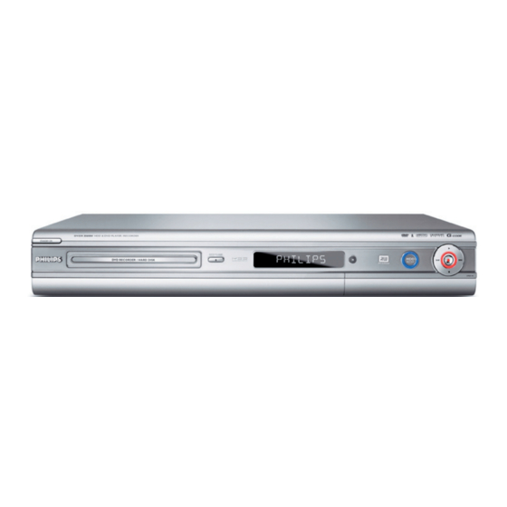
Philips DVDR3350H Service Manual
Dvd-video recorder
Hide thumbs
Also See for DVDR3350H:
- User manual (101 pages) ,
- Specifications (2 pages) ,
- Quick start manual (2 pages)
Table of Contents
Advertisement
Quick Links
DVD-Video Recorder
CLASS 1
LASER PRODUCT
Contents
1
2
3
4
5
6
7
© Copyright 2005 Philips Consumer Electronics B.V. Eindhoven, The Netherlands.
All rights reserved. No part of this publication may be reproduced, stored in a
retrieval system or transmitted, in any form or by any means, electronic,
mechanical, photocopying, or otherwise without the prior permission of Philips.
Published by KC-TE 0549 AV Systems
Version 1.0
DVDR3350H/DVDR3360H/DVDR3370H
DVDR3350H/37/55, DVDR3360H/75/96/97
Contents
Page
2
4
6
9
12
23
23
24
25
26
27
8
28
29
30
30
31
32
33
34
35
9
36
37
38
39
40
Printed in the Netherlands
& DVDR3370H/75/96/97
Subject to modification
Page
41
42
42
43
43
43
44
45
46
47
48
49
50
51
51
52
52
56
59
59
59
64
75
75
76
EN 3139 785 31500
Advertisement
Table of Contents

Related Manuals for Philips DVDR3350H


Summary of Contents for Philips DVDR3350H
-
Page 1: Table Of Contents
Layout: Analog-Main Part (Bottom View) Front: Front Panel - Display © Copyright 2005 Philips Consumer Electronics B.V. Eindhoven, The Netherlands. All rights reserved. No part of this publication may be reproduced, stored in a retrieval system or transmitted, in any form or by any means, electronic, mechanical, photocopying, or otherwise without the prior permission of Philips. -
Page 2: Technical Specifications And Connection Facilities
Frequency response at Cinch (L+R) Test equipment: Fluke 54200 TV Signal generator output : 100 Hz - 10 kHz / 0 ± Test streams: Philips Standard test pattern S/N according to DIN 45405, 7, 1967 1.4.1 System and PHILIPS standard test pattern : ≥... -
Page 3: Digital Output
Technical Specifi cations and Connection Facilities 3139 785 31500 EN 3 Analogue Inputs / Outputs Audio Performance CD 1.5.1 External In (Rear) 1.7.1 Cinch Output Rear Video - Y/C (Hosiden) Output voltage 2 channel mode : 2Vrms ± 1dB according IEC 933-5 Channel unbalance (1kHz) : <1dB Superimposed DC-level on pin 4 (load ≥... -
Page 4: Safety Information, General Notes & Lead Free Requirements
EN 4 3139 785 31500 Safety Information, General Notes & Lead Free Requirements Safety Information, General Notes & Lead Free Requirements Safety Instructions Warnings 2.1.1 General Safety 2.2.1 General Safety regulations require that during a repair: • All ICs and many other semiconductors are susceptible to •... - Page 5 “Video Plus+” and “PlusCode” are registered trademarks of workshop during a repair: the Gemstar Development Corporation. The “Video Plus+” • Use only lead-free solder alloy Philips SAC305 with order system is manufactured under licence from the Gemstar Development Corporation. code 0622 149 00106. If lead-free solder-pate is required, please contact the manufacturer of your solder-equipment.
-
Page 6: Directions For Use
Directions For Use The following except of the Quick Use Guide serves as an introduction to the set. The Complete Direction for the Use can be downloaded in different languages from the internet site of Philips Customer care Center: www.p4c.philips.com... - Page 7 Directions For Use 3139 785 31500 EN 7...
- Page 8 EN 8 3139 785 31500 Directions For Use...
-
Page 9: Mechanical Instructions
Mechanical Instructions 3139 785 31500 EN 9 Mechanical Instructions Dismantling and Assembly of the Set 4.1.2 Dismantling of the Hard-Disk Drive & Front Panel Assembly For item numbers please see the exploded view in Chapter 9. 1) Remove the 4 screws from the Hard-Disk Drive. 4.1.1 Dismantling of the DVD Loader Tray Cover 1) Inserting a minus screw driver and push the lever in the... - Page 10 EN 10 3139 785 31500 Mechanical Instructions 3) Remove the 6 screws to remove the front plate 184 3) Place the Basic Engine in the service position by fl ipping as shown in Figure 4-5. the basic engine to the vertical position. Figure 4-5 Figure 4-7 4.1.3...
- Page 11 Mechanical Instructions 3139 785 31500 EN 11 2) Service Position can be achieved by fl ipping the Digital 3) Service Position can be achieved by fl ipping the Analog board to the Vertical Position as shown in Figure 4-9. board to the Vertical Position as shown in Figure 4-10. Figure 4-12 Figure 4-9 Note: The cable (just to transfer the service connection to the...
-
Page 12: Upgrade Software & Repair Chart
Remove disc from tray & reset system 7. Remove the Upgrade Disc and press <OK> button to confi rm 8. The TV screen goes blank, tray close and after a while the Philips Logo screen appear again. C. Procedure to apply the HDD fi rmware upgrade: 1. - Page 13 EN 13 7. Remove the Upgrade Disc and press <OK> button to confi rm. 8. The TV screen goes blank, tray close and after a while the Philips Logo screen appear again. 9. Press <Tuner> and <Setup>. 10. In “SETUP MENU – HDD”, select “Delete HDD” and press <OK>...
- Page 14 EN 14 Upgrade Software & Repair Chart 3139 785 31500 NOTES: 1. For references to voltage levels, NOK represents voltage measurements that are outside the range of +-10% of specifi ed values 2. For references to soldering touch ups and replacing components, OK means the set no longer shows the problem and is working fi...
- Page 15 Upgrade Software & Repair Chart 3139 785 31500 EN 15 Repair Chart 5.3.1 Completely Dead Set Visible problems with connections Check all cable connections for visible disconnections Fix the cable connections or loose connections No visible problems with connections Check Voltage at Digital Board Connector 1501 Pin 1=3.30v Pin 2 =3.30v Pin 3 =3.30v...
- Page 16 EN 16 Upgrade Software & Repair Chart 3139 785 31500 5.3.2 Cannot Read Disk Visible problems with connections Check supply cable from PSU Connector J5 to Drive 4 pin connector for visible Fix the cable connection disconnections or loose connections No visible problems with connections Visible problems with...
- Page 17 Upgrade Software & Repair Chart 3139 785 31500 EN 17 5.3.4 Audio No Sound (Playback) NOTE1: To start debugging this section, playback in repeat mode a 1kHz 0dB sine wave from a test CD NOTE2: All references are to Analog Board unless otherwise specified Visible problems with Check cables on connector 1600 and 1400 connections...
- Page 18 EN 18 Upgrade Software & Repair Chart 3139 785 31500 5.3.5 Audio No Sound (TV & External Source) NOTE1: To start debugging this section, playback a 0dB 1kHz sine wave from a test disc on the external source which exhibits the problem. NOTE2: All references are to Analog Board unless otherwise specified Visible problems with connections...
- Page 19 Upgrade Software & Repair Chart 3139 785 31500 EN 19 Part 2 Check I310 & I311 Check MSP (7500) Xtal at I509 = Verify against Truth Table below 18.432MHz Check Supply voltage at F420 = 8V I508 = 5V I515 = 5V IF MDX 7301 pin 3 &...
- Page 20 EN 20 Upgrade Software & Repair Chart 3139 785 31500 5.3.6 No Video Out Upon Power ON (Assume set is not dead) NOTE: To verify that the set is not dead, you should be able to do the following. 1. See on the Front Display the words “Ch001” after the required boot up time has elapsed 2.
- Page 21 Upgrade Software & Repair Chart 3139 785 31500 EN 21 5.3.7 No Video In Only NOTE1: All references are to Digital Board unless otherwise specified NOTE2: For problem with Rear Video Input, refer to Section1. For problem with Front Video Input, go to Section2. Section1 Section2 Visible loose...
- Page 22 EN 22 Upgrade Software & Repair Chart 3139 785 31500 5.3.8 Tuner Not Functioning NOTE: All references are to Analog Board Check for visible cracks on PCB at the areas near Replace Analog Board to the Tuner Check Voltage at testpoints Replace PSU I119 = 33V F101 = 5V...
-
Page 23: Block Diagrams,Waveforms, Wiring Diagram
Block Diagrams, Waveforms, Wiring Diagram. 3139 785 31500 EN 23 Block Diagrams, Waveforms, Wiring Diagram Overall Block Diagram of the Set ANALOG BOARD Front Keyboards 1201 CONTROL LINES, AND SUPPLY LINES CONTROL LINES 1922 AFCRI AFCLI CVBSFIN AUDIO L CONTROL UNIT SLAVE CFIN MICROPROCESSOR YFIN... -
Page 24: Control Block Diagram
Block Diagrams, Waveforms, Wiring Diagram. 3139 785 31500 EN 24 Control Block Diagram Control Block Diagram Analog Board Front FAN_CTRL Keys I2C Bus Front Panel Processor Level Shifter NEC uPD-16316GBT Reset HOST_Reset >=1 Reset 5VSTBY Supply Display FRONT Board IDE0 DVDR Multi Sound RSA1,RSA2... -
Page 25: Wiring Diagram
3139 785 31500 EN 25 Wiring Diagram DVDR3350H, DVDR3360H and DVDR3370H Note: To see the pin assignments, open the corresponding group by clicking the [+] / [-] icon(s) next to the left margin. Hide all groups to see block diagram and interconnections in one screen. -
Page 26: Waveforms Of Analog Board
Block Diagrams, Waveforms, Wiring Diagram. 3139 785 31500 EN 26 Waveforms Waveforms of Analog Board F219 Y_OUT F220 C_OUT F222 CVBS_OUT F236 D_C F237 D_Y F238 D_VR F239 D_YG F240 D_UB I302 AFER I304 AFEL I619 ALDAC I621 ARDAC I714 D_OUT 7500MSP XTAL_IN 7500MSP XTAL_OUT... -
Page 27: Waveforms Of Digital Board
Block Diagrams, Waveforms, Wiring Diagram. 3139 785 31500 EN 27 Waveforms of Digital Board AUD_BCKI T537 AUD_BOKO T541 AUD_DAI(0) T539 AUD_DAO(0) T543 AUD_MCKI T540 AUD_MCKO T544 AUD_WCKI T538 AUD_WCKO T542 VOA_BPb T518 VOA_GY T520 VOA_RPr T521 VOA_SY T522 VOA_SC T523 VOA_CVBS T524... -
Page 28: Test Point Overview For Analog Board
Block Diagrams, Waveforms, Wiring Diagram. 3139 785 31500 EN 28 Test Points Overview for Analog Board Testpoint_AnalogBd_32694.pdf 2005-11-18... -
Page 29: Test Point Overview For Digital Board
Block Diagrams, Waveforms, Wiring Diagram. 3139 785 31500 EN 29 Test Points Overview for Digital Board Testpoint_DigitalBd_32683.pdf 2005-11-18... -
Page 30: Circuit Diagram And Pwb Layout
Circuit Diagrams and PWB Layouts 3139 785 31500 EN 30 Circuit Diagrams and PWB Layouts Analog: Frontend Video (FV) 0803 H7 1100 F1 1101 C1 2100 B6 2101 A11 from PS 2102 F5 5VSTBY 33VSTBY 2103 F6 2104 F6 2105 H3 2106 H3 5V_FV VIDOUT... -
Page 31: Analog: Video In / Out (Iov)
Circuit Diagrams and PWB Layouts 3139 785 31500 EN 31 Analog: Video In / Out (IOV) 1201-1 I13 F204 C2 1201-3 C13 F205 E3 1202 E2 F206 E3 1203 F13 F207 G2 1204 H2 F208 G2 1205 I7 F209 G2 1206 I6 F210 H2 1207-1 C1... -
Page 32: Analog: Audio In / Out (Ioa)
Circuit Diagrams and PWB Layouts 3139 785 31500 EN 32 Analog: Audio In / Out (IOA) 1201-2 E9 1207-2 A1 2300 A3 2301 A2 2302 B3 2303 B2 REAR IN 1 2304 B2 2305 C2 2306 A5 F300 2300 2307 A5 2308 D2 2309 D2 2310 D2... -
Page 33: Analog: Power Supply (Ps)
Circuit Diagrams and PWB Layouts 3139 785 31500 EN 33 Analog: Power Supply (PS) 1400 A1 2412 B5 2417 E4 3403 F2 3408 G5 5400 B5 7400 F2 7405 A4 F404 A2 F409 B2 F414 B2 F419 H6 2352 G4 2413 D4 2418 E5 3404 F1... -
Page 34: Analog: Multi Sound Processing (Msp)
Circuit Diagrams and PWB Layouts 3139 785 31500 EN 34 Analog: Multi Sound Processing (MSP) 1500 F6 2500 A1 2501 C1 2502 C1 2503 E2 from PS 8VSTBY 2504 E2 8VSTBY 2505 A5 2506 A5 2507 A6 2508 A6 2509 A6 2510 B8 I512 I513... -
Page 35: Analog: Audio Converter (Dac_Adc)
Circuit Diagrams and PWB Layouts 3139 785 31500 EN 35 Analog: Audio Converter (DAC_ADC) 1600 C1 F606 D2 2600 B1 F607 D1 2603 D3 F608 D1 2604 D3 F609 D1 2605 D4 F610 D1 2606 D4 F611 E1 2607 E1 F612 E1 5VSTBY 2608 E1... -
Page 36: Analog: Digital In / Out 1 (Digio 1)
Circuit Diagrams and PWB Layouts 3139 785 31500 EN 36 Analog: Digital In / Out 1 (DIGIO 1) 0006 F2 1700 C9 1701 D9 2700 A4 2701 A4 2702 D2 2703 E5 2704 D5 2705 D8 2706 D7 3700 A3 I712 3701 A4 3702 B4... -
Page 37: Analog: Control Unit (Cu)
Circuit Diagrams and PWB Layouts 3139 785 31500 EN 37 Analog: Control Unit (CU) 0005 E1 1800 C1 1803 B3 1804 E4 2800 E3 3800 D1 3801 E1 3802 E2 3803 E2 3804 F2 frm/to Dig Board 3805 E3 3806 E3 3807 F3 HLW20S-2C7 3808 D2... -
Page 38: Layout: Analog-Main Part (Top View)
Circuit Diagrams and PWB Layouts 3139 785 31500 EN 38 Layout: Analog-Main Part (Top View) TopView_AnalogBd_32694.pdf 2005-11-18... -
Page 39: Layout: Analog-Main Part (Bottom View)
Circuit Diagrams and PWB Layouts 3139 785 31500 EN 39 Layout: Analog-Main Part (Bottom View) TopView_AnalogBd_Hmc_32694.pdf 2005-11-18... -
Page 40: Front: Front Panel - Display
Circuit Diagrams and PWB Layouts 3139 785 31500 EN 40 Front: Front Panel - Display 0100 F2 3138 H10 I110 H9 1100 D6 3139 G9 I111 H10 1101 D5 3140 G10 I112 H10 1201 D13 4102 F1 I113 H10 12VSTBY 1203 1203 A7 4103 F2... -
Page 41: Front: Front Panel - Audio/Video In
Circuit Diagrams and PWB Layouts 3139 785 31500 EN 41 Front: Front Panel - Audio/Video-In 1202 B1 1218 F3 1219 E2 1300 D3 1301 D1 3200 1401 E1 5VSTBY 5ESD 1402 E1 2200 A2 2201 A2 2202 A2 2203 A3 2204 C1 2205 D3 2206 E2... -
Page 42: Layout: Front Panel (Top Copper Pattern)
Circuit Diagrams and PWB Layouts 3139 785 31500 EN 42 Layout: Front Panel (Top Copper Pattern) - SMD + Components TopView_FrontBd_32673.pdf 2005-11-18 Layout: Front Panel (Bottom Copper Pattern) - Components TopView_FrontBd_Hmc1_32673.pdf 2005-11-18... -
Page 43: Front: Standby
Circuit Diagrams and PWB Layouts 3139 785 31500 EN 43 Front: Standby Layout: Standby (Top View) Layout: Standby (Bottom View) 0013 C2 1303 C4 2300 D2 6300 D3 6301 D3 F300 C2 F301 C2 STANDBY BOARD I300 C4 0013 1303 I300 F300 EVQ11L05R... -
Page 44: Digital: Back-End Processor
Circuit Diagrams and PWB Layouts 3139 785 31500 EN 44 Digital: Back-End Processor 1101 B6 3169 F9 1105 E5 3171-1 G10 1111 D6 3171-2 G10 2101 B6 3171-3 G10 2102 B6 3171-4 G10 2105 E8 3172-1 G10 Back-end Processor 2106 E5 3172-2 G10 3V3BE Communication (COM) -
Page 45: Digital: Memory
Circuit Diagrams and PWB Layouts 3139 785 31500 EN 45 Digital: Memory 2201 D2 3275-4 E12 2202 D2 3277-1 F12 2203 D3 3277-2 F12 2204 D4 3277-3 F12 2205 D3 3277-4 F12 Memory 2211 B5 3281-1 F12 2212 B5 3281-2 F12 2213 B5 3281-3 F12 2214 B5... -
Page 46: Digital: Ieee 1394 Physical Layer
Circuit Diagrams and PWB Layouts 3139 785 31500 EN 46 Digital: IEEE 1394 Physical Layer 1351 D5 1351 D5 2301 D6 2301 D6 2302 D6 2302 D6 2303 D6 2303 D6 2304 D6 2304 D6 2305 D7 2305 D7 IEEE1394 Physical Layer 2306 D7 2306 D7 2307 D7... -
Page 47: Digital: Video Input Processor
Circuit Diagrams and PWB Layouts 3139 785 31500 EN 47 Digital: Video Input Processor 1461 D7 T435 F10 2401 C9 T461 D7 2402 C9 T462 E7 2403 C9 2404 C9 2411 B9 Video Input Processor 2412 B9 2413 B9 2414 B9 2415 B10 2421 B7 2422 B7... -
Page 48: Digital: Interfaces
Circuit Diagrams and PWB Layouts 3139 785 31500 EN 48 Digital: Interfaces 1501 C1 3575-4 G2 T537 A13 1502 I13 3576-1 G2 T538 A13 1511 A7 3576-2 G2 T539 A13 1512 A8 3576-3 G2 T540 B13 1521 A10 3576-4 H2 T541 B13 1522 A10 3577 H2... -
Page 49: Layout: Digital-Main Part (Top View)
Circuit Diagrams and PWB Layouts 3139 785 31500 EN 49 Layout: Digital-Main Part (Top View) TopView_DigitalBd_32683.pdf 2005-11-18... -
Page 50: Layout: Digital-Main Part (Bottom View)
Circuit Diagrams and PWB Layouts 3139 785 31500 EN 50 Layout: Digital-Main Part (Bottom View) BottomView_DigitalBd_32683.pdf 2005-11-18... -
Page 51: Circuit- And Ic Description
Circuit- and IC description 3139 785 30981 EN 51 Circuit- and IC description • 8.1. PSU Board Connector B: Supply to Digital Board 8.1.1. General Pin no. Supply / Signal Remarks 3V3D No component, No copper This screw can 3V3D track area 30.5+/-0.15 be used as EMC... -
Page 52: Front Board
EN 52 3139 785 30981 Circuit- and IC Description 8.2. Front Board (Panel – Display + Key) 8.3. Analog Board 8.2.1. General 8.3.1. General The PCBA consist of the following parts: • This board consists of the following parts: Fan Control •... - Page 53 Circuit- and IC description 3139 785 30981 EN 53 8.3.4. Audio routing Figure 8-2 Analog Audio IO...
- Page 54 EN 54 3139 785 30981 Circuit- and IC Description The sound processing is always done in stereo (that means separate left- and right- channel) and the complete switching is realized by using HEF4052, which is a dual four-to-one multiplexer and MSP3415G, multi-sound processor.
- Page 55 Circuit- and IC description 3139 785 30981 EN 55 8.3.6. Video routing Figure 8-3 Analog Video IO...
-
Page 56: Digital Board
EN 56 3139 785 30981 Circuit- and IC Description The switching of the various video input signals is done video encorder, and provides build-in support for non- by the Video Input Processor on the Digital Board. These simultaneous progressive and interlaced video output. A signals are directly routed to the digital board through 1394 link layer function is also integrated, requiring only connector 1205 on the Analog Board... - Page 57 Circuit- and IC description 3139 785 30981 EN 57 Video Part Front-end I The analogue video input signals CVBS (Rear, Front, The Domino chip interfaces directly to the basic Engine Tuner) and YC (Front) are routed via the board to via ATAPI connector 1571.
- Page 58 EN 58 3139 785 30981 Circuit- and IC Description 8.4.5. Power Supply • 2.5V supply for the SDRAM is generated by an ultra The Digital board is not powered in standby mode. The fast low dropout linear regulator [7515] control signal STBY on the analog board will enable the •...
-
Page 59: Power Supply Unit
Circuit- and IC description 3139 785 30981 EN 59 8.5. Power Supply Unit • to Digital Board 8.5.1. The following are the various supply lines provided: • 12VD to Digital Board • 3V3STBY to Analog Board • to Basic Engine •... - Page 60 EN 60 3139 785 30981 Circuit- and IC Description PIN DESCRIPTION AND CONFIGURATION SYMBOL PIN DESCRIPTION supply voltage ground handbook, halfpage V CC DRAIN CTRL control input input from auxiliary winding for TEA1507 demagnetization timing, OVP and OPP CTRL DRIVER programmable current sense input I sense sense...
- Page 61 Circuit- and IC description 3139 785 30981 EN 61 PIN CONFIGURATION VREF1 DACM_L SC1_OUT_R DACM_R SC1_OUT_L VREF2 AHVSUP 33 32 31 30 29 28 27 26 25 24 23 CAPL_M RESETQ AHVSS I2S_DA_IN2 AGNDC DVSS SC2_IN_L DVSUP SC2_IN_R ADR_CL MSP 34x5G I2S_DA_IN1 SC1_IN_L I2S_DA_OUT...
- Page 62 EN 62 3139 785 30981 Circuit- and IC Description PIN DESCRIPTION AND CONFIGURATION SDIN SCLK AMUTEC LRCK AOUTA MCLK VA_H AOUTB DIF1(SCL/CCLK) BMUTEC DIF0(SDA/CDIN) DEM(AD0/CS) VBIAS Pin Name Pin Description SDIN Serial Audio Data Input ( Input ) - Input for two’s complement serial audio data. SCLK Serial Clock ( Input ) - Serial clock for the serial audio interface.
- Page 63 Circuit- and IC description 3139 785 30981 EN 63 IC7606 - 96KHz Sampling 24-bit stereo audio ADC BLOCK DIAGRAM V DDA V SSA V RP V RN V ref SYSCLK V DDD UDA1361TS V SSD V INL ΣΔ MSSEL DECIMATION CLOCK FILTER CONTROL...
-
Page 64: Digital Board
EN 64 3139 785 30981 Circuit- and IC Description 8.6.2 Digital Board IC7301 - IEEE 1394a-2000 one port cable Transceiver/Arbiter BLOCK DIAGRAM Received Data Decoder/Retimer Link CNA † Interface SYSCLK LREQ TPA+ CTL0 TPA– CTL1 Cable Port TPB+ Arbitration and Control TPB–... - Page 65 Circuit- and IC description 3139 785 30981 EN 65 PIN CONFIGURATION PHP package terminal diagram PHP PACKAGE (TOP VIEW) 47 46 45 44 43 40 39 38 AGND SYSCLK CTL0 CTL1 AGND TPBIAS TSB41AB1 TPA+ TPA– TPB+ TPB– AGND 14 15 17 18 19 20 21 22 23 24 Figure 8-13...
-
Page 66: Pin Description
EN 66 3139 785 30981 Circuit- and IC Description PIN DESCRIPTION TERMINAL TYPE TYPE DESCRIPTION DESCRIPTION NAME PHP NO. AGND 26, 32, 36 Supply – Analog circuit ground terminals. These terminals should be tied together to the low-impedance circuit board ground plane. AV DD 25, 35 Supply... - Page 67 Circuit- and IC description 3139 785 30981 EN 67 TERMINAL TYPE TYPE DESCRIPTION DESCRIPTION NAME PHP NO. DGND 14, 46, 47 Supply – Digital circuit ground terminals. These terminals should be tied together to the low-impedance circuit board ground plane. DV DD 21, 44, 45 Supply...
- Page 68 EN 68 3139 785 30981 Circuit- and IC Description TERMINAL TYPE TYPE DESCRIPTION DESCRIPTION NAME PHP NO. PLLGND Supply – PLL circuit ground terminals. These terminals should be tied together to the low-impedance circuit board ground plane. PLLV DD Supply –...
- Page 69 Circuit- and IC description 3139 785 30981 EN 69 IC7401 - 4x10bit DigitalVideo Decoder with microvision BLOCK DIAGRAM Copy CVBS/Y/G Protection Data Detector Slicer Analog Front End VI_1_A Composite and S-Video Processor CVBS/ VI_1_B ADC1 Pb/B/C VI_1_C Luma CVBS/Y Separation Processing YCbCr 5-line...
- Page 70 EN 70 3139 785 30981 Circuit- and IC Description PIN DESCRIPTION TERMINAL DESCRIPTION DESCRIPTION NAME NUMBER Analog Video VI_1_A VI_1_x: Analog video input for CVBS/Pb/B/C VI_1_B VI_2_x: Analog video input for CVBS/Y/G VI_1_C VI_3_x: Analog video input for CVBS/Pr/R/C VI_2_A VI_4_A: Analog video input for CVBS/Y VI_2_B Up to 10 composite, 4 S-video, and 2 composite or 3 component video inputs (or a combination thereof)
- Page 71 Circuit- and IC description 3139 785 30981 EN 71 TERMINAL DESCRIPTION DESCRIPTION NAME NUMBER Host Interface I 2 C clock input I 2 C data bus Power Supplies AGND Analog ground. Connect to analog ground. A18GND_REF Analog 1.8-V return A18VDD_REF Analog power for reference 1.8 V CH1_A18GND CH2_A18GND...
-
Page 72: Top View
EN 72 3139 785 30981 Circuit- and IC Description IC7501 - Power Distribution Switches BLOCK DIAGRAM Power Switch † Charge Pump Current Driver Limit UVLO Thermal Sense † Current Sense Figure 8-16 PIN CONFIGURATION TPS2041 D OR P PACKAGE (TOP VIEW) Figure 8-17... - Page 73 Circuit- and IC description 3139 785 30981 EN 73 PIN DESCRIPTION TERMINAL DESCRIPTION DESCRIPTION NAME D OR P TPS2041 TPS2051 – Enable input. Logic low turns on power switch. – Enable input. Logic high turns on power switch. Ground 2, 3 2, 3 Input voltage Over current.
- Page 74 EN 74 3139 785 30981 Circuit- and IC Description IC7595 - Voltage Detector Series with Programmable Delay BLOCK DIAGRAM NCP303LSNxxT1 Open Drain Output Configuration Input Reset Output Figure 8-18 PIN DESCRIPTION AND CONFIGURATION PIN CONNECTIONS AND MARKING DIAGRAM Reset Output Input N.C.
-
Page 75: Exploded View & Spare Parts List
Exploded View & Spare Parts List 3139 785 31500 EN 75 Exploded View of the Set Figure 9-1... -
Page 76: Spare Parts List
CAB. FRONT ASSY DVDR3370H/75 0011 3139 247 11652 PSU 05H80 WR DVDR33570H/75, /96, /97 ONLY 0021 3139 248 85821 PCBAS DVDR3350H ANA BOARD NA P002 3141 079 34271 COVER TRAY ASSY DVDR 3350H/37 /37, /55, /96 ONLY P003 3141 079 34261... - Page 77 Exploded View & Spare Parts List 3139 785 31500 EN 77 DIODES PCBAS DVDR3350H ANA BOARD AP (DVDR3360H/75/97 & DVDR3370H/75/97 ONLY) 6200 9322 129 41685 BZM55-C12 MISCELLANEOUS 6201 9322 129 41685 BZM55-C12 1101 2422 542 00025 TUN IF V U PLL IEC BGIDKL B...
- Page 78 3492 2350 035 10229 RST NETW SM ARV24 4X22R PM5 R 3573 3198 031 13390 RST NETW 1206 4X 33R PM5 COL PCBAS DVDR3350H DIGI BOARD NA (DVDR3350H/37 ONLY) 3574 3198 031 13390 RST NETW 1206 4X 33R PM5 COL MISCELLANEOUS...
- Page 79 7595 9322 165 15685 IC SM NCP303LSN30 (ONSE) R 3684 3198 031 13390 RST NETW 1206 4X 33R PM5 COL PCBAS DVDR3350H DIGI BOARD LA (DVDR3350H/55 ONLY) MISCELLANEOUS 1101 2422 543 01502 RES XTL 13MHZ5 16P AT-49 A 1351 2422 543 01503...
- Page 80 RST NETW 1206 4X 33R PM5 COL 7595 9322 165 15685 IC SM NCP303LSN30 (ONSE) R 3684 3198 031 13390 RST NETW 1206 4X 33R PM5 COL PCBAS DVDR3350H DIGI BOARD/96 (DVDR3360H/96 & DVDR3370H/96 ONLY) MISCELLANEOUS 1101 2422 543 01502 RES XTL 13MHZ5 16P AT-49 A...
- Page 81 7595 9322 165 15685 IC SM NCP303LSN30 (ONSE) R 3684 3198 031 13390 RST NETW 1206 4X 33R PM5 COL PCBAS DVDR3350H DIGI BOARD AP (DVDR3360H/75/97 & DVDR3370H/75/97 ONLY) MISCELLANEOUS 1101 2422 543 01502 RES XTL 13MHZ5 16P AT-49 A...
- Page 82 Exploded View & Spare Parts List EN 82 3139 785 31500 COILS & FILTERS PCBAS DVDR3350H FRONT BOARD MISCELLANEOUS 5121 4822 157 11717 BLM31P500SPT 5135 4822 157 11499 BLM11P600SPT 1100 2422 540 00014 RES CER 5MHZ CSTLS*G53 A 5141 4822 157 11717...
- Page 83 7103 4822 130 41246 BC327-25 7104 9322 229 34671 IC SM UPD16316GB-007-8ET-A Y 7106 3198 010 42310 BC847BW 7107 9322 185 95667 IR RECEIVER TSOP4836 (VISH)L 7108 3198 010 42310 BC847BW PCBAS DVDR3350H STANDBY BOARD 1303 4822 276 13732 SWITCH TACT PUSH...