Table of Contents
Troubleshooting

Related Manuals for Panasonic KX-FT931LA-B


Summary of Contents for Panasonic KX-FT931LA-B
- Page 1 Order No.KMF0605960CE Personal Facsimile KX-FT931LA-B B: Black Version (for Latin America) © 1995 Matsushita Electric Industrial Co., Ltd. All rights reserved. Unauthorized copying and distribu- tion is a violation of law.
-
Page 2: Table Of Contents
KX-FT931LA-B TABLE OF CONTENTS PAGE PAGE 1 Safety Precautions -----------------------------------------------3 15.2. Gear Section --------------------------------------------- 130 1.1. For Service Technicians ----------------------------------3 15.3. Jams ------------------------------------------------------- 136 1.2. AC Caution---------------------------------------------------4 15.4. Cleaning--------------------------------------------------- 137 1.3. Personal Safety Precautions ----------------------------5 16 Miscellaneous -------------------------------------------------- 138 16.1. Terninal Guide of the ICs, Transistors and 1.4. -
Page 3: Safety Precautions
KX-FT931LA-B 1 Safety Precautions 1. Before servicing, unplug the AC power cord to prevent an electric shock. 2. When replacing parts, use only the manufacturer's recommended components. 3. Check the condition of the power cord. Replace if wear or damage is evident. -
Page 4: Ac Caution
KX-FT931LA-B 1.1.2. How to recognize that Pb Free Solder is Used P.C.Boards marked as “PbF” use Pb Free solder. (See the figure below.) (Example:Digital board) Note: The “PbF” marked may be found on different areas of the same P.C.Board,depending on manufacture date. -
Page 5: Personal Safety Precautions
KX-FT931LA-B 1.3. Personal Safety Precautions 1.3.1. Moving Sections of the Unit Be careful not to let your hair, clothes, fingers, accessories, etc., become caught in any moving sections of the unit. The moving sections of the unit are the rollers and a gear. There is a separation roller and a document feed roller which are rotated by the document feed motor. -
Page 6: Service Precautions
KX-FT931LA-B 1.4. Service Precautions 1.4.1. Precautions to Prevent Damage from Static Electricity Electrical charges accumulate on a person. For instance, clothes rubbing together can damage electric elements or change their electrical characteristics. In order to prevent static electricity, touch a metallic part that is grounded to release the static... -
Page 7: Warning
KX-FT931LA-B 2 Warning 2.1. About Lead Free Solder (PbF: Pb free) Note: In the information below, Pb, the symbol for lead in the periodic table of elements, will refer to standard solder or solder that con- tains lead. We will use PbF solder when discussing the lead free solder used in our manufacturing process which is made from Tin, (Sn), Silver, (Ag), and Copper, (Cu). -
Page 8: Specifications
KX-FT931LA-B 3 Specifications Applicable Lines: Public Switched Telephone Network Document Size: Max. 216 mm in width Max. 600 mm in length Effective Scanning Width: 208 mm 216 × max. 30 m roll Recording Paper Size: Effective Printing Width: 208 mm Transmission Time* Approx. -
Page 9: General/Introduction
KX-FT931LA-B 4 General/Introduction 4.1. Optional Accessories Model No. Item Specifications/Usage 216 mm × 30 m roll, with 25 mm core KX-A106 Standard thermal recording paper* Use only the included or specified recording paper. Using other recording paper may affect print quality and/or cause excessive wear to the thermal head. -
Page 10: Features
KX-FT931LA-B 4.2.3. Error Message (Display) 5 Features 5.1. Integrated Telephone System • Redialing function General • Phonebook function (100 names) • LCD (Liquid Crystal Display) readout • Caller ID compatible** **Feature requires a subscription to caller identification ser- Facsimile vices offered by certain local telephone companies for a tee. -
Page 11: Technical Descriptions
KX-FT931LA-B 6 Technical Descriptions 6.1. Connection Diagram... -
Page 12: General Block Diagram
KX-FT931LA-B 6.2. General Block Diagram The following is an outline of each device IC on the digital board. (Refer to General Block Diagram (P.13).). 1. ASIC (IC1) Composed mainly of an address decoder and a modem control. Controls the general FAX operations. - Page 13 KX-FT931LA-B 6.2.1. General Block Diagram...
-
Page 14: Control Section
KX-FT931LA-B 6.3. Control Section 6.3.1. ASIC (IC1) This custom IC is used for the general FAX operations. 1. CPU: KB for the image processing. This model uses a Z80 equivalent to the CPU operating 7. THERMAL HEAD I/F: at 12 MHz. Most of the peripheral functions are performed Transmits the recorded data to the thermal head. - Page 15 KX-FT931LA-B SIGNAL POWER SUPPLIED DESCRIPTION VOLTAGE VDD (3.3V) ----- POWER SOURCE (+3.3V) MIDAT/IOP 3.3V PORT (TONE1EN) MICLK/IOP 3.3V OUTPUT PORT (TONE2EN) MILAT/IOP 3.3V PORT (HSRXEN) 20KOSC/IOP 3.3V OUTPUT PORT (PWRCNT) XWAIT 3.3V INPUT PORT (HOOK) HSTRD/IOP 3.3V INPUT PORT (TEST) HSTWR/IOP 3.3V...
- Page 16 KX-FT931LA-B SIGNAL POWER SUPPLIED DESCRIPTION VOLTAGE STB2 3.3V STROBE SIGNAL OUTPUT TO THERMAL HEAD STB3 3.3V OUTPUT PORT (NC) XRESET 3.3V RESET INPUT VDD (3.3V) ----- POWER SOURCE (+3.3V) POWER SOURCE (GND) POWER SOURCE (GND) VDD (3.3V) ----- POWER SOURCE (+3.3V) XORESET 3.3V...
- Page 17 KX-FT931LA-B 6.3.2. Flash Memory (IC2) This 512KB ROM (FLASH MEMORY) carries a common area of 32KB and bank areas which each have 8KB (BK4~BK63). The addresses from 0000H to 7FFFH are for the common area and from 8000H to 9FFFH are for the bank areas.
- Page 18 KX-FT931LA-B 6.3.5. RTC Back up Circuit 1. Function This unit has a lithium battery (BAT1) which works for the Real Time Clock (RTC, Integrated into ASIC:IC1). The RTC continues functioning, even when the power switch is OFF, backed up by a lithium battery.
- Page 19 KX-FT931LA-B 6.3.6. Supervision Circuit for the Thermal Head Temperature 1. Function The thermistor changes the resistor according to the temperature and uses the thermistor's characteristics. The output of pin 139 of IC1 becomes a low level. Then when it becomes a high level, it triggers point A. In point C, according to the voltage output time, the thermal head's temperature is detected.
-
Page 20: Facsimile Section
KX-FT931LA-B 6.4. Facsimile Section 6.4.1. Image Dara Flow During Facsimile Operation Copy (Fine, Super-Fine, Photo) 1. Line information is read by CIS (to be used as the reference white level) via route (1), and is input to IC1. Refer to Block Dia- gram (P.21) - Page 21 KX-FT931LA-B 6.4.2. Block Diagram...
-
Page 22: Thermal Head
KX-FT931LA-B 6.4.3. Thermal Head 1. Function This unit utilizes state of the art thermal printer technology. The recording paper (roll paper) is chemically processed. When the thermal head contacts this paper it emits heat momen- tarily, and black dots (appearing like points) are printed on the paper. If this continues, letters and/or diagrams appear, and the original document is reproduced. - Page 23 KX-FT931LA-B...
- Page 24 KX-FT931LA-B 6.4.4. Scanning Block The scanning block of this device consists of a control circuit and a contact image sensor made up of a celfoc lens array, a light source, and photoelectric conversion elements. When an original document is inserted and the start button pressed, pin 129 of IC1 goes to a high level and the transistor Q14 turns on.This applies voltage to the light source to light it.
- Page 25 KX-FT931LA-B 6.4.5. Stepping Motor Drive Circuit 1. Function One individual stepping motor is used for transmission and reception. It feeds the document or recording paper synchronized for reading or printing. 2. Circuit Operation During motor drive, ASIC IC1 pin 124 becomes a high level, and Q2 and Q1 go ON as a result. +24 V is supplied tothe motor coil.
-
Page 26: Sensors And Switches
KX-FT931LA-B 6.5. Sensors and Switches All of the sensors and switches are shown below. Sensor Circuit Sensor Sensor or Switch Name Message Error Location DIGITAL Motor Position Sensor [CALL SERVICE] ANALOG Recording Paper Sensor [CHECK COVER] and [OUT OF PAPER] Hook SW ————... - Page 27 KX-FT931LA-B 6.5.1. Motor Position Sensor This sensor is a detection switch for recording the position of the CAM. Digital Board Signal (IC1-119 Pin) Home position Low level Other High level 6.5.2. Recording Paper Sensor (SW1) When there is no recording paper, the plate is separated from the switch lever and the switch turns off. Pin 20 of IC1 becomes a high level.
- Page 28 KX-FT931LA-B 6.5.3. Hook Switch (SW2) When the handset is lifted, the switch turns ON, and the signal at pin 43 of IC1 becomes low. When the handset is returned, the switch turns OFF, and the signal at pin 43 of IC1 becomes high.
- Page 29 KX-FT931LA-B 6.5.5. Document Top Sensor (SW39) When a document is brought to the read position, the SW becomes ON, and the input signal of IC1-5 pin (Operation) becomes a low level. When there is no document at the read position, the SW becomes OFF, and the input signal of IC1-5 pin (Operation) becomes a high level.
-
Page 30: Modem Section
KX-FT931LA-B 6.6. Modem Section 6.6.1. Function The unit uses a 1 chip modem (IC5) that serves as an interface between the control section for FAX transmission and reception and the telephone line. During a transmitting operation, the digital image signals are modulated and sent to the telephone line. - Page 31 KX-FT931LA-B Phase A: Call setting Call setting can be manual/automatic. Phase B: Pre-message procedure Phase B is a pre-processing procedure and sequence for confirming the status of the terminal, transmission route, etc., and for terminal control. It implements terminal preparation status, determines and displays terminal constants, confirms synchroniza- tion status, etc.
- Page 32 KX-FT931LA-B 6. Explanation of Communication and Compression Technology a. G3 Communication Signals (T. 30 Binary Process) For G3 Facsimile communication, this is the procedure for exchanging control signals between the sending and receiving machines both before and after transmission of image signals.
- Page 33 KX-FT931LA-B Bit No. DIS/DTC Receiver --- T.4 operation Receiver --- T.4 operation 11,12,13,14 Data signaling rate Data signaling rate 0,0,0,0 V.27 ter fall back mode 2400 bit/s, V.27 ter 4800 bit/s, V.27 ter 0,1,0,0 V.27 ter 1,0,0,0 V.29 9600 bit/s, V.29 1,1,0,0 V.27 ter and V.29...
- Page 34 KX-FT931LA-B Bit No. DIS/DTC Reserved for future recording width capability. Extend field Extend field R8×15.4 lines/mm R8×15.4 lines/mm 300×300 pels/25.4 mm 300×300 pels/25.4 mm R16×15.4 lines/mm and/or 400×400 pels/25.4 mm R16×15.4 lines/mm and/or 400×400 pels/25.4 mm Inch based resolution preferred Resolution type selection “0”: neritic based resolution...
- Page 35 KX-FT931LA-B b. Redundancy Compression Process Coding Mode This unit uses one-dimensional MH format.
- Page 36 KX-FT931LA-B 6.6.2. Modem Circuit Operation The modem (IC5) has all the hardware satisfying the CCITT standards mentioned previously. When the ASIC IC1 (61) is brought to a low level, the modem (IC5) is chip-selected and the resistors inside IC are selected by the select signals from ASIC (IC1) ADR0-ADR4.
-
Page 37: Ncu Section
KX-FT931LA-B 6.7. NCU Section 6.7.1. General It is composed of bell detection circuit, pulse dial circuit, line amplifier, sidetone circuits. 6.7.2. Bell Detection Circuit 1. Circuit Operation The signal waveform for each point is indicated below. The signal (low level section) input to pin 23 of ASIC IC1 on the digital board. - Page 38 KX-FT931LA-B 6.7.5. Line Amplifier and Side Tone Circuits 1. Circuit Operation The reception signal received as output from line transformer T1 is given as input to R81, C17, R13 and IC2(2). Then it is input to the reception system at an amplifier gain of 2.5 dB from pin (2).
- Page 39 KX-FT931LA-B 6.7.6. Calling Line Identification Circuit 1. Function This unit is compatible with the Caller ID service offered by your local telephone company. To use this feature, you must sub- scribe to a Caller ID service. The data for the caller ID from the telephone exchange is sent during the interval between the first and second rings of the bell signal.
- Page 40 KX-FT931LA-B 6.7.7. Calling Line Identification Circuit (DTMF) 1. Function This unit is compatible with the Caller ID service offered by your local telephone company. To use this feature, you must sub- scribe to a Caller ID service. The data for the Caller ID from the telephone exchange is sent before the first ring signal. The data from the telephone exchange is sent by DTMF signal.
-
Page 41: Its (Integrated Telephone System) And Monitor Section
KX-FT931LA-B 6.8. ITS (Integrated Telephone System) and Monitor Section 6.8.1. General The general ITS operation is performed by the modem IC5. The alarm tone, the key tone, the calling tone and the beep are output from the ASIC IC1 (digital board). - Page 42 KX-FT931LA-B 6.9.2. Circuit Diagram R26 R27 R22 R23 R14 R15...
-
Page 43: Operation Board Section
(IC1) and ASIC (IC1: on the DIGITAL BOARD). The key matrix table is shown below. (Chip on board type) ASIC CN206 GATE ARRAY KEYS KIN0~7 MATRIX XLED8, 9 XLED13 READ POSITION SENSOR DOCUMENT SENSOR DIGITAL BOARD OPERATION BOARD KX-FT931LA-B OPERATION BOARD: BLOCK DIAGRAM... -
Page 44: Lcd Section
KX-FT931LA-B 6.11. LCD Section The Gate Array IC(IC1) works only for writing the ASCII code from the data bus (D4~D7). V0 is supplied for the crystal drive. R25, R24, R15 and R17 are density control resistors. Consequently, in this unit, the timing (positive clock) is generated by the LCD interface circuitry in the gate array (IC1). -
Page 45: Power Supply Board Section
KX-FT931LA-B 6.12. Power Supply Board Section This power supply board uses the switching regulator method. Block Diagram Input Input Rectifier Circuit Output Circuit Kick-on Circuit Voltage Circuit Over Converter voltage Circuit A-B Voltage Wave Form Surge 9~6V absorber circuit Output... - Page 46 KX-FT931LA-B The following is an overview of how the power supply unit is controlled. The control method of this power supply unit is pulse width modulation. When Q is ON, the energy is charged in the transfer primary coil according to E .
- Page 47 KX-FT931LA-B [Surge Absorber Circuit] This circuit is for absorbing surge voltage generated by the Q1. [Control Circuit and Detecting Circuit] The control circuit amplifies the output with increased voltage detected in the error detecting circuit. Then it drives the main transis- tor.
-
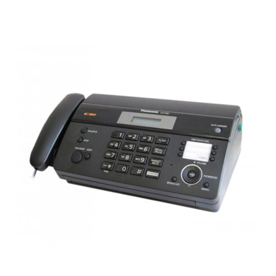
Page 48: Location Of Controls And Components
KX-FT931LA-B 7 Location of Controls and Components 7.1. Overview (1) Speaker (2) Document guides (3) Document feeder tray (4) Top cover (5) Document exit (6) Document entrance (7) Top cover release button... -
Page 49: Control Panel
KX-FT931LA-B 7.2. Control Panel Buttons (1) [CALLER ID] (10) [PAUSE] • To use Caller ID features. • To insert a pause during dialing. (2) [STOP] (11) [MONITOR] • To stop an operation or programming session. • To initiate dialing without lifting the handset. -
Page 50: Installation Instructions
KX-FT931LA-B 8 Installation Instructions 8.2. Connections Important: 8.1. Installation Space • The unit will not function when there is a power failure. To make calls in emergency situations, you should con- The space required to install the unit is shown below. -
Page 51: Installing The Recording Paper
KX-FT931LA-B 8.3. Installing the Recording Paper 5. Close the top cover securely by pushing down on both sides. 1. Open the top cover by pressing the top cover release but- ton ( 6. Press [FAX/START], then tear off the excess paper by 2. -
Page 52: Operation Instructions
KX-FT931LA-B 9 Operation Instructions 9.1. Setting Your Logo Your logo will be printed on the top of each page sent from your unit. The logo can be your name or the name of your company. Note: Refer to Other (P.9) for display message. - Page 53 KX-FT931LA-B To select characters with dial keypad 3. Press [5] 3 times. 4. Press [ ] to move the cursor to the next space and press [5] 3 times. To change uppercase or lowercase letters Pressing the [ ] button will change to uppercase or lower- case letters alternately.
-
Page 54: Test Mode
KX-FT931LA-B 10 Test Mode The codes listed below can be used to perform simple checks for some of the unit’s functions. When complaints are received from customers, they provide an effective tool for identifying the locations and causes of malfunctions. To do this, you set the Service mode (Refer to Operation Flow (P.56).) first, then operate the below test items. -
Page 55: Dtmf Single Tone Transmit Selection
KX-FT931LA-B 10.1. DTMF Single Tone Transmit Selection When set to ON (=1), the 12 keys and transmission frequencies are as shown. High Frequency (Hz) Low Frequency (Hz) High (Hz) 1209 1336 1477 “1” “5” 1209 Low (Hz) “2” “6” 1336 “1”... -
Page 56: Service Mode
KX-FT931LA-B 11 Service Mode The programming functions are used to program the various features and functions of the machine, and to test the machine. This facilitates communication between the user and the service man while programming the unit. 11.1. Programming and Lists 11.1.1. - Page 57 KX-FT931LA-B 11.1.3. Service Function Table Code Function Set Value Effective Default Remarks Range Pause time X 100 msec 001~600 ---------- Flash time X 10 ms 01~99 ---------- Dial speed select 1: 10 pps 1, 2 ---------- 1: 20 pps Bell detection time...
- Page 58 KX-FT931LA-B Code Function Set Value Effective Default Remarks Range Receive error limit value set 1: 5 % Sets the number of acceptable error lines when the 2: 10 % FAX reconstructs the received data. Refer to Receive 3: 15 % Problem (P.81).
-
Page 59: The Example Of The Printed List
KX-FT931LA-B 11.2. The Example of the Printed List 11.2.1. User Mode (Example of a printed out list) Note: The above values are the default values. - Page 60 KX-FT931LA-B 11.2.2. Service Mode Settings (Example of a printed out list) Note: The above values are the default values.
- Page 61 KX-FT931LA-B 11.2.3. History (Example of a printed out list) Note: See the following descriptions of this report. Item No. (1) ~ (44) are corresponding to the listed items in Descriptions of the History Report (P.62).
- Page 62 KX-FT931LA-B 11.2.3.1. Descriptions of the History Report (31) Not used (1) SOFTWARE VERSION FLASH ROM version (32) NUMBER OF DIVIDED PRINTING IN FAX RECEPTION (2) SUM The number of faxes received that were divided into more than FLASH ROM internal data calculation.
-
Page 63: Troubleshooting Guide
KX-FT931LA-B 12 Troubleshooting Guide 12.1. Troubleshooting summary 12.1.1. Troubleshooting After confirming the problem by asking the user, troubleshoot according to the instructions and observe the following precautions. 12.1.2. Precautions 1. If there is a problem with the print quality or the paper feed, first check if the installation space and the print paper meets the specifications, the paper selection lever/paper thickness lever is set correctly, and the paper is set correctly without any slack. -
Page 64: Error Messages-Display
KX-FT931LA-B 12.2. Error Messages-Display If the unit detects a problem, one or more of the following Erase unnecessary items. messages will appear on the display. The explanations given in the [ ] are for servicemen only. Note: Refer to Error Message (Display) (P.10) for display mes- •... -
Page 65: Error Messages Report
KX-FT931LA-B 12.3. Error Messages Report 12.3.1. Journal Report 1. Press [MENU] repeatedly to display “PRINT REPORT”. 2. Press [ ] or [ ] until the “JOURNAL REPORT” is displayed. 3. Press [SET]. 4. The report is printed out. Note: Refer to Error Message (Report) (P.9) for display message. - Page 66 KX-FT931LA-B...
- Page 67 KX-FT931LA-B CROSS REFERENCE: Test Mode(P.54)
- Page 68 KX-FT931LA-B CROSS REFERENCE: Test Mode(P.54)
- Page 69 KX-FT931LA-B CROSS REFERENCE: Test Mode(P.54)
- Page 70 KX-FT931LA-B...
- Page 71 KX-FT931LA-B CROSS REFERENCE: Maintenance(P.128) ADF (Auto Document Feed) Section(P.92) Operation Panel Section(P.167) CROSS REFERENCE: Test Mode(P.54)
- Page 72 KX-FT931LA-B...
- Page 73 KX-FT931LA-B...
- Page 74 KX-FT931LA-B CROSS REFERENCE: Test Mode(P.54)
- Page 75 KX-FT931LA-B 12.3.2. Special service journal reports Journal 2 and Journal 3 shown below, which are special journals giving the additional detailed information about the latest 30 communications, can be printed by Service Code 881 or 882. Remote printing function for the journal reports (JOURNAL, JOURNAL 2 and JOURNAL 3) is also available for service technicians.
- Page 76 KX-FT931LA-B 12.3.2.1. Journal 2 Refer to JOURNAL 2 in Printout Example(P.77). Journal 2 displays the additional detailed information about the last 30 communications. Descriptions: (1) RCV. MODE Indicates which receive mode the unit was in when the unit received a fax message.
- Page 77 KX-FT931LA-B 12.3.2.2. Journal 3 Refer to JOURNAL 3 in Printout Example (P.77). (9) ERROR LINE(RX) Descriptions: When an error occurs while receiving a fax, this shows the (6) ENCODE number of error lines. Compression Code: MH/MR (10) MAKER CODE (7) MSLT This shows a 2 digit code of the other party's fax machine MSLT means Minimum Scan Line Time.
- Page 78 KX-FT931LA-B 12.3.3. Communication Section Find the problem in the table shown below, and refer to the corresponding troubleshooting procedure in Defective Facsimile Section (P.79). Symptom Content Possible cause The paper is not fed properly when faxing. Troubleshooting Problem with the feeding mecha- (Nor in the copy mode.)
- Page 79 KX-FT931LA-B 12.3.3.1. Defective Facsimile Section 12.3.3.1.1. Transmit Problem CROSS REFERENCE: Operation Panel Section(P.112) ADF (Auto Document Feed) Section(P.92) Maintenance(P.128)
- Page 80 KX-FT931LA-B 12.3.3.1.2. Sometime there is a transmit problem Note: Refer to Error Message (Display) (P.10) for display message. Note: • “596: Transmit level set” represents a service code. (Refer to Service Function Table(P.57).)
- Page 81 KX-FT931LA-B 12.3.3.1.3. Receive Problem First confirm whether the recording paper is installed properly or not before starting troubleshooting. (Refer to “Remarks”.) Note: “596: Transmit level set” represents a service code. (Refer to Service Function Table (P.57).) Remarks: Regarding the reception problem, we have investigated the conceivable causes in the flow chart except for the software-related errors.
- Page 82 KX-FT931LA-B 12.3.3.1.4. The unit can copy, but cannot transmit/receive CROSS REFERENCE: Analog Board Section(P.107) Test Mode(P.54)
- Page 83 KX-FT931LA-B 12.3.3.1.5. The unit can copy, but cannot either transmit/receive long distance or interna- tional communications The following two causes can be considered for this symptom. Cause 1: The other party is executing automatic dialing, the call has been received by this unit, and the CED or DIS signal response time is too long.
- Page 84 KX-FT931LA-B (Causes and Countermeasures) Countermeasure Side Echo Communication Problem Example Countermeasure Service Code Sending side Some time is needed to compare the level Add a dummy signal to the beginning of Service code (521) of the receiving and sending signals for the the training signal.
- Page 85 KX-FT931LA-B Fig. c (Countermeasure by Changing the Interval Between CED and DIS) Fig. d (Countermeasure by Ignoring the 1st DIS) <TX side signal> <RX side signal> <Countermeasure> 2nd / 3rd DCS / Training & delayed CFR / FTT at TX side 2nd / 3rd EOP / EOM / MPS &...
- Page 86 KX-FT931LA-B 12.3.3.1.7. How to record fax signal by using PC Recording FAX signal is one of the useful analysis measures to solve communication problems. The way of recording easily by using PC is shown as follows. 1. Equipment • 1 jig Parts No.
-
Page 87: Remote Programming
KX-FT931LA-B 12.4. Remote Programming If, after the call is connected, the customer describes the situation and it is determined that the problem can be corrected by making parameter changes, this function makes it possible to change parameters such as the user code and service code from another fax (using DTMF tones). - Page 88 KX-FT931LA-B 12.4.2. Program Mode Table Code Function Set Value Default Remote Set- ting Set date and time dd/mm/yy hh:mm 01/01/06 Your logo --------- None Your FAX number --------- None Print sending report 1:ON / 2:OFF / 3:ERROR ERROR FAX ring count 1-4 / 5: EXT.TAM...
- Page 89 KX-FT931LA-B Code Function Set Value Default Remote Set- ting Sensor test --------- --------- Print test pattern --------- --------- Top margin 1~9 mm DTMF ON time 060~200 10ms DTMF OFF time 060~200 10ms History list 1:SET --------- Journal 2 1:SET ---------...
-
Page 90: Troubleshooting Details
KX-FT931LA-B 12.5. Troubleshooting Details 12.5.1. Outline Troubleshooting is for recovering quality and reliability by determining the broken component and replacing, adjusting or clean- ing it as required. First, determine the problem then decide the troubleshooting method. If you have difficulty finding the broken part, determine which board is broken. - Page 91 KX-FT931LA-B 12.5.3. Troubleshooting Items ITEM SYMPTOM REFERENCE No feed See No Document Feed (P.92) (Auto Document Feeder) Paper jam See Document Jam (P.93) Multiple feed See Multiple Feed (P.94) Skew See Skew (P.95) Printing Skewed receiving image. See Skewed Receiving Image (P.97) Image is distorted.
- Page 92 KX-FT931LA-B 12.5.4. ADF (Auto Document Feed) Section 12.5.4.1. No Document Feed Note: (*1) : Refer to Multiple Feed (P.94) (*2) : Refer to How to Remove the Operation Board, LCD and Platen Roller (P.120) (*3) : Refer to Test Mode (P.54) (*4) : Refer to Digital Board Section (P.99)
-
Page 93: Document Jam
KX-FT931LA-B 12.5.4.2. Document Jam CROSS REFERENCE: Test Mode (P.54) Sensor Section (P.113) Note: (*1) : Refer to How to Remove the Operation Board, LCD and Platen Roller (P.120) (*2) : Refer to Disassembly and Assembly Instructions (P.117) - Page 94 KX-FT931LA-B 12.5.4.3. Multiple Feed Note: (*1) : Refer to How to Remove the Separation Holder and Document Feed Support (P.121) (*2) : Refer to Disassembly and Assembly Instructions (P.117) (*3) : Refer to Maintenance (P.128)
- Page 95 KX-FT931LA-B 12.5.4.4. Skew Note: (*1) : Refer to Maintenance Items and Componet Locations (P.128) (*2) : Refer to Disassembly and Assembly Instructions (P.117) (*3) : Refer to How to Remove the Separation Holder and Document Feed Support (P.121) (*4) : Refer to How to Remove the Operation Board, LCD and Platen Roller (P.120)
- Page 96 KX-FT931LA-B 12.5.4.5. Image is Distorted (When printing) CROSS REFERENCE: Thermal Head Section (P.115). Test Mode(P.54) CIS (Contact Image Sensor) Section (P.114). Note: (*1) : Refer to Maintenance Items and Componet Locations (P.128) (*2) : Refer to Disassembly and Assembly Instructions (P.117)
- Page 97 KX-FT931LA-B 12.5.4.6. Black or White Vertical Lines Appear CROSS REFERENCE: Test Mode(P.54) Digital Board Section (P.99) Note: (*1) : Refer to How to Remove the Lock Lever and Thermal Head (P.123) (*2) : Refer to Maintenance Items and Componet Locations (P.128) (*3) : Refer to How to Remove the Operation Board, LCD and Platen Roller (P.120)
- Page 98 KX-FT931LA-B 12.5.4.8. When Coping or Printing, an Abnormal Sound is Heard from the Unit Note: (*1) : Refer to Document Feeder Cleaning (P.137) (*2) : Refer to Thermal Head Cleaning (P.137) (*3) : Refer to Disassembly and Assembly Instructions (P.117) (*4) : Refer to How to Remove the Motor of Gear Block (P.126)
-
Page 99: Digital Board Section
KX-FT931LA-B 12.5.5. Digital Board Section When the unit fails to boot up the system, take the troubleshooting procedures very carefully. It may have a serious problem. The symptom: No response when the power is turned on. (No LCD display, and keys are not accepted.) The first step is to check the power source. - Page 100 KX-FT931LA-B 12.5.5.1. Digital Block Diagram Digital board is including analog system. All analog signals (Telephone, CID and TAM) excepting Fax communications. Another one is ASIC system for mechanical functions: Copy, Fax and UI (LCD/Key). And serial interface (UART) connects both systems.
- Page 101 KX-FT931LA-B NG Wave pattern Note: Refer to NG Example (P.106).
- Page 102 KX-FT931LA-B Normal Wave Patterns Remarks: When you use an oscilloscope to judge whether a signal to be tested is normal or NG, perform the signal check in exactly the same order as in [List 1]. (If the ASIC fails to access the ROM, the ASIC cannot access DRAM normally.) The digital circuit actually operates according to the timing combinations of these signals.
- Page 103 KX-FT931LA-B I/O and Pin No. Diagram...
- Page 104 KX-FT931LA-B 12.5.5.2. Check the Status of the Digital Board First, please check voltages and oscillation whether they are correct as follows.
- Page 105 KX-FT931LA-B...
- Page 106 KX-FT931LA-B 12.5.5.3. NG Example...
- Page 107 KX-FT931LA-B 12.5.6. Analog Board Section This chapter provides the testing procedures required for the analog parts. A signal route to be tested is determined depending upon purposes. For example, the handset TX route begins at the handset microphone and the signal is output to the telephone line.
- Page 108 KX-FT931LA-B 12.5.6.2. Defective ITS (Integrated Telephone System) Section 1. No handset and monitor transmission / reception Following the ITS section or NCU section, search for the route between the microphone and the telephone line (sending) or between the telephone line and the speaker (receiving) where the signal disappears.
- Page 109 KX-FT931LA-B 12.5.7. Power Supply Board Section 12.5.7.1. Key components for troubleshooting Check the following parts first: F1, D10-D13, C5, and Q1. This comes from our experience with experimental tests. For example: power supply and lightning surge voltage test, withstanding voltage test, intentional short circuit test, etc.
- Page 110 KX-FT931LA-B 12.5.7.2. Troubleshooting Flow Chart...
- Page 111 KX-FT931LA-B 12.5.7.3. Broken Parts Repair Details (D10, D11, D12, D13) Check for a short-circuit in terminal 4. If D10, D11, D12 and D13 are short-circuits, F1 will melt (open). In this case, replace all of the parts (D10, D11, D12, D13, F1).
- Page 112 KX-FT931LA-B 12.5.8. Operation Panel Section 12.5.8.1. No Key Operation CROSS REFERENCE: Test Mode(P.54) 12.5.8.2. No LCD Indication CROSS REFERENCE: Test Mode(P.54)
- Page 113 KX-FT931LA-B 12.5.9. Sensor Section Refer to Sensors and Switches (P.26) for the circuit descriptions. 12.5.9.1. Check the Document Sensor (SW39)....“CHECK DOCUMENT” Note: Refer to Error Message (Display) (P.10) for display message. 12.5.9.2. Check the Read Position Sensor (SW38)....“REMOVE DOCUMENT” Note:...
- Page 114 KX-FT931LA-B 12.5.10. CIS (Contact Image Sensor) Section Refer to Scanning Block (P.24). CROSS REFERENCE: Test Mode(P.54)
- Page 115 KX-FT931LA-B 12.5.11. Thermal Head Section Refer to Thermal Head(P.22).
-
Page 116: Service Fixture & Tools
KX-FT931LA-B 13 Service Fixture & Tools... -
Page 117: Disassembly And Assembly Instructions
KX-FT931LA-B 14 Disassembly and Assembly Instructions 14.1. Disassembly Flowchart 14.1.1. Upper Cabinet Section CROSS REFERENCE: A-1 : How to Remove the Operation Panel Block (P.119) A-2 : How to Remove the Operation Board, LCD and Platen Roller (P.120) A-3 : How to Remove the Separation Holder and Document Feed Support (P.121) A-4 : How to Remove the Image Sensor (CIS) and Feed Roller (P.122) -
Page 118: Lower Cabinet Section
KX-FT931LA-B 14.1.2. Lower Cabinet Section CROSS REFERENCE: B-1 : How to Remove the Bottom Frame (P.124) B-2 : How to Remove the Analog Board, Digital Board, Power Supply Board and Power Cord (P.125) B-3 : How to Remove the Gear Block and Separation Roller (P.126) -
Page 119: Disassembly Procedurel
KX-FT931LA-B 14.2. Disassembly Procedurel 14.2.1. How to Remove the Operation Panel Block... - Page 120 KX-FT931LA-B 14.2.2. How to Remove the Operation Board, LCD and Platen Roller...
- Page 121 KX-FT931LA-B 14.2.3. How to Remove the Separation Holder and Document Feed Support...
- Page 122 KX-FT931LA-B 14.2.4. How to Remove the Image Sensor (CIS) and Feed Roller...
- Page 123 KX-FT931LA-B 14.2.5. How to Remove the Lock Lever and Thermal Head...
- Page 124 KX-FT931LA-B 14.2.6. How to Remove the Bottom Frame...
- Page 125 KX-FT931LA-B 14.2.7. How to Remove the Analog Board, Digital Board, Power Supply Board and Power Cord...
- Page 126 KX-FT931LA-B 14.2.8. How to Remove the Gear Block and Separation Roller 14.2.9. How to Remove the Motor of Gear Block...
- Page 127 KX-FT931LA-B 14.2.10. Installation Position of the Lead Wires...
-
Page 128: Maintenance
KX-FT931LA-B 15 Maintenance 15.1. Maintenance Items and Componet Locations 15.1.1. Outline MAINTENANCE AND REPAIRS ARE PERFORMED USING THE FOLLOWING STEPS. 1. Periodic maintenance Inspect the equipment periodically and if necessary, clean any contaminated parts. 2. Check for breakdowns Look for problems and consider how they arose. - Page 129 KX-FT931LA-B 15.1.2.1. Maintenance List OPERATION CHECK REMARKS Document Path Remove any foreign matter such as paper. ---------- Rollers If the roller is dirty, clean it with a damp cloth then dry thoroughly. Refer to How to Remove the Image Sensor (CIS) and Feed Roller (P.122).
-
Page 130: Gear Section
KX-FT931LA-B 15.2. Gear Section This section shows how the motor-driven gear mechanism works in the main operations: FAX transmission, FAX reception the motor and copying. 15.2.1. Mode Selection When the motor attached to the Drive Motor Gear rotates counterclockwise (CCW), Swing Gear A engages the CAM and the CAM turns counterclockwise to select a mode. - Page 131 KX-FT931LA-B 15.2.2. Mode Operation Once a mode is selected, the Drive Motor Gear rotates clockwise (CW) and then the Swing Gear A-1 controls the mode opera- tion. 15.2.2.1. TX Mode Swing Gear A engages Gear TX and conveys its drive power to the Separation Roller Gear for pre-feeding documents.
-
Page 132: Copy Mode
KX-FT931LA-B 15.2.2.3. Copy Mode Swing Gear A and B engage Gear TX and Gear RX respectively and drive both the Separation Roller Gear and the Platen Roller Gear for feeding documents and recording paper in the copying operation. Fig. D: Copy mode 15.2.2.4. - Page 133 KX-FT931LA-B 15.2.3. Mechanical Movements in the Main Operations 15.2.3.1. Idle Status...
- Page 134 KX-FT931LA-B 15.2.3.2. Scanning 15.2.3.3. Printing Note: See Sensors and Switches (P.26) CROSS REFERENCE: Sensor Section (P.113) Error Messages-Display (P.64)
- Page 135 KX-FT931LA-B 15.2.3.4. Copying CROSS REFERENCE: Sensor Section (P.113)
-
Page 136: Jams
KX-FT931LA-B 15.3. Jams 15.3.1. Recording Paper Jams 15.3.2. Document Jams - Sending 1. Open the top cover by pressing the top cover release but- 1. Open the top cover by pressing the top cover release but- ton ( ton ( ) and remove the jammed document carefully 2. -
Page 137: Cleaning
KX-FT931LA-B 15.4. Cleaning 15.4.2. Thermal Head Cleaning If smudges or black/white lines appear on a copied/received 15.4.1. Document Feeder Cleaning document, check whether there is dust on the thermal head. Clean the document feeder when: Clean it to remove the dust. -
Page 138: Miscellaneous
KX-FT931LA-B 16 Miscellaneous 16.1. Terninal Guide of the ICs, Transistors and Diodes 16.1.1. Digital Board 16.1.2. Analog Board 16.1.3. Operation Board... -
Page 139: Power Supply Board
KX-FT931LA-B 16.1.4. Power Supply Board... -
Page 140: How To Replace The Flat Package Ic
KX-FT931LA-B 16.2. How to Replace the Flat Package IC Even if you do not have the special tools (for example, a spot heater) to remove the Flat IC, with some solder (large amount), a soldering iron and a cutter knife, you can easily remove the ICs that have more than 100 pins. -
Page 141: Bridge Modification Procedure
KX-FT931LA-B 2. Apply flux to all pins of the FLAT PACKAGE IC. 3. Solder the pins, sliding the soldering iron in the direction of the arrow. 16.2.4. Bridge Modification Procedure 1. Lightly resolder the bridged portion. 2. Remove the remaining solder along the pins using a soldering iron as shown in the figure below. -
Page 142: Test Chart
KX-FT931LA-B 16.3. Test Chart 16.3.1. ITU-T No.1 Test Chart... - Page 143 KX-FT931LA-B 16.3.2. ITU-T No.2 Test Chart...
- Page 144 KX-FT931LA-B MEMO:...
-
Page 145: Schematic Diagram
KX-FT931LA-B 17 Schematic Diagram 17.1. Digital Board 4M DRAM 4M FLASH MOTOR BLOCK FOR PROGRAM A[4] D[0] A[5] D[1] A[6] D[2] A[0] A[0] D[0] A[7] D[3] A[1] A[1] D[1] RBA[0] D[4] A[2] A[2] D[2] D[0] RBA[1] D[5] +24V A[3] A[3]... - Page 146 XCLK/EYEXY EYESYNC EYECLK 2.7K (21) EYE PATTERN MONITOR C207 TEST PAD K1000p SPMUTE CIS BLOCK (22) +3.3VD R142 TO SPEAKER IC12 (23) +5V TO +2V +5VA C143 K1000p C140 R140 R141 9.1K K0.1u KX-FT931LA-B : DIGITAL BOARD SCHEMATIC DIAGRAM (24)
-
Page 147: Analog Board
KX-FT931LA-B 17.2. Analog Board +24VA 110K +2.0V J220p 300:600 K0.047u 50V4.7u K0.047u +12V 110K J220p 510K +24V J27p K0.033u +24V J82p 560K +2.0V PAPER LINETX TONE1 (10) K0.1u K0.022u Z0.1u P_SHORT BELL/DCN 1A2K HOOK (11) LINERX MONRX H/STX_MUTE (12) H/SRX (13) 6.8K... - Page 148 (PU AT DIGITAL BOARD) TO EXT. TEL 250V1u 15K 1/2W (10) 5.6K K0.068u 1K2A +24V (11) RLY1 K0.1u (12) J220p 620K K0.027u (13) K0.027u +2.0V FLT3 1 HSMIC- 2 HSSP+ 3 HSSP- 4 HSMIC+ (14) K0.1u 16V10u KX-FT931LA-B : ANALOG BOARD SCHEMATIC DIAGRAM...
-
Page 149: Operation Board
KX-FT931LA-B 17.3. Operation Board... -
Page 150: Power Supply Board
KX-FT931LA-B 17.4. Power Supply Board... - Page 151 KX-FT931LA-B MEMO:...
-
Page 152: Printed Circuit Board
KX-FT931LA-B 18 Printed Circuit Board 18.1. Digital Board 18.1.1. Component View... - Page 153 KX-FT931LA-B 18.1.2. Bottom View...
-
Page 154: Analogue Board
KX-FT931LA-B 18.2. Analogue Board 18.2.1. Component View ZNR1 PCB-CH RLY1 AUTO-CH PFUP1547Z... - Page 155 KX-FT931LA-B 18.2.2. Bottom View EXT.LINE +12V PFUP1547Z...
-
Page 156: Operation Board
KX-FT931LA-B 18.3. Operation Board 18.3.1. Component View... - Page 157 KX-FT931LA-B 18.3.2. Bottom View...
-
Page 158: Power Supply Board
KX-FT931LA-B 18.4. Power Supply Board J102 D105 J103 D110 C109 J101 D7 D17 54D1 BOND R111 R112 R115 C410 R409 R410 Q101 D104 R119 R122 ZNR1 R121 R412 R411 WHITE BLACK/ /BLUE BROWN... -
Page 159: Appendix Information Of Schematic Diagram
KX-FT931LA-B 19 Appendix Information of Schematic Diagram Note: 1. DC voltage measurements are taken with an oscilloscope or a tester with a ground. 2. The schematic diagrams and circuit board may be modified at any time with the development of new technology. - Page 160 KX-FT931LA-B MEMO...
-
Page 161: Exploded View And Replacement Parts List
KX-FT931LA-B 20 Exploded View and Replacement Parts List 20.1. Cabinet, Mechanical and Electrical Parts Location 20.1.1. Operation Panel Section... -
Page 162: Upper Cabinet Section
KX-FT931LA-B 20.1.2. Upper Cabinet Section... - Page 163 KX-FT931LA-B 20.1.3. Lower Cabinet Section...
- Page 164 KX-FT931LA-B 20.1.4. Gear Block Section...
- Page 165 KX-FT931LA-B 20.1.5. Screws...
- Page 166 KX-FT931LA-B 20.1.6. Accessories and Packing Materials...
-
Page 167: Replacement Parts List
KX-FT931LA-B 20.2. Replacement Parts List Ref. Part No. Part Name & Description Remarks Notes: PFKR1086Z1 GUIDE, LEFT 1. The marking (RTL) indicates that the Retention Time is PFUV1088Z2 COVER, DOCUMENT GUIDE PFHX1834Z READ SHEET (WHITE PLATE) limited for this item. -
Page 168: Digital Board Parts
KX-FT931LA-B 20.3.4. Gear Block Section Ref. Part No. Part Name & Description Remarks C3ABKC000034 C1CB00001959 Ref. Part No. Part Name & Description Remarks B1HAGFF00015 C0ABEB000052 PFDG1447Z GEAR,TX4 IC10 C0JBAS000252 PFDG1444Z GEAR,TX1 IC11 C0JBAA000474 PFDG1446Z GEAR,TX3 IC12 C1BB00000129 PFDG1445Z GEAR,TX2 PFDG1442Z... - Page 169 KX-FT931LA-B Ref. Part No. Part Name & Description Remarks Ref. Part No. Part Name & Description Remarks C125 ECJ1VB1C104K K5H251200003 FUSE C127 ECJ1VC1H101J 100P C128 ECJ1VB1C104K (COILS) C129 ECJ1VF1E104Z PQLQR2KA113 COIL C140 ECJ1VB1C104K PQLQR2KA113 COIL C142 F2G1H4R70017 PQLQR2KA20T COIL C143 ECJ1VB1H102K 0.001...
-
Page 170: Analog Board Parts
KX-FT931LA-B 20.5. Analog Board Parts Ref. Part No. Part Name & Description Remarks R112 ERJ3GEYJ334 330K R123 ERJ3GEYJ104 100K Ref. Part No. Part Name & Description Remarks R124 ERJ3GEYJ473 R125 ERJ3GEYJ222 2.2K PCB2 PFLP1754LAZ ANALOG BOARD ASS'Y (RTL) R126 ERJ3GEYJ393... -
Page 171: Operation Board Parts
KX-FT931LA-B Ref. Part No. Part Name & Description Remarks Ref. Part No. Part Name & Description Remarks ERJ3GEY0R00 ECJ1VB1H392K 0.0039 ERJ3GEY0R00 F2A1C1000030 ERJ3GEY0R00 ECJ1VB1C473K 0.047 ERJ3GEY0R00 ECJ1VB1H682K 0.0068 ERJ3GEY0R00 ECJ1VB1C473K 0.047 ERJ3GEY0R00 ECJ1VF1E104Z ERJ6GEYJ1R0 ECJ1VB1C473K 0.047 ECJ1VC1H270J ERJ3GEYJ101 ECJ2VF1H104Z ERJ3GEYJ103 ECJ1VB1C223K 0.022... -
Page 172: Power Supply Board Parts
KX-FT931LA-B Ref. Part No. Part Name & Description Remarks Ref. Part No. Part Name & Description Remarks SW20 EVQ11Y05B SPECIAL SWITCH PFVDERA9102 DIODE(SI) SW21 EVQ11Y05B SPECIAL SWITCH 1SS355F DIODE(SI) SW22 EVQ11Y05B SPECIAL SWITCH 1SS355F DIODE(SI) SW23 EVQ11Y05B SPECIAL SWITCH MA8091... -
Page 173: Fixtures And Tools
KX-FT931LA-B Ref. Part No. Part Name & Description Remarks PFCKD31E225 PFCKD2C1H101 100P PFCKD31E105 C411 PFCKD71H224 0.22 C101 PFCEA35L330M C102 PFCEA16ZL470 C109 DEHC32H471 470P C115 PFCKDB31H104 20.8. Fixtures and Tools Ref. Part No. Part Name & Description Remarks PQZZ9K7Z EXTENSION CORD, 9 PIN...