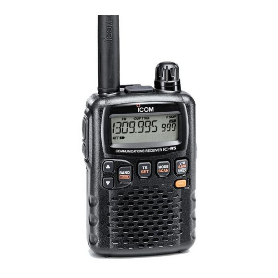
Icom IC-R5 Service Manual
Coomunications receiver
Hide thumbs
Also See for IC-R5:
- Supplementary manual (1 page) ,
- Instruction manual (80 pages) ,
- Instruction manual (9 pages)
Table of Contents
Advertisement
Quick Links
Download this manual
See also:
Instruction Manual
Advertisement
Table of Contents

Related Manuals for Icom IC-R5


Summary of Contents for Icom IC-R5
- Page 1 SERVICE MANUAL COMMUNICATIONS RECEIVER...
- Page 2 INTRODUCTION This service manual describes the latest service information for the IC-R5 COMMUNICATIONS RECEIVER at the time of publication. MODEL Version SYMBOL AC ADAPTER Europe BC-149D U.K. Italy U.S.A. BC-149A IC-R5 France BC-149D Spain BC-149D Export-01 EXP-01 BC-136A Export-02 EXP-02...
-
Page 3: Table Of Contents
TABLE OF CONTENTS SECTION SPECIFICATIONS SECTION INSIDE VIEWS SECTION DISASSEMBLY INSTRUCTIONS SECTION CIRCUIT DESCRIPITON RECEIVER CIRCUITS ........... . .4-1 PLL CIRCUITS . - Page 4 SECTION 1 SPECIFICATIONS GENERAL RECEIVER • Receiver system : Tripple super heterodyne • Frequency range • Intermediate frequency : 1st 266.7 MHz Version Receive Frequencies (MHz) 2nd 19.65 MHz EUR, U.K., 450 kHz ITA, ESP, CAN 0.495 – 1309.995 • Sensitivity* : (except spurious points) EXP-01, EXP-02 Frequency (MHz)
- Page 5 SECTION 2 INSIDE VIEWS • LOGIC UNIT EEROM (IC2: CAT24WC256) AF mute switch (Q350: 2SJ144) AF power amplifier (IC450: TA31056F) AF filter (Q301: XP6501) Battery charger circuit +3.2 regurater D503: MA133 (IC103: R1111N321B) D500: SB07-03C Q501: 2SB-1132 DC-DC convertor IC102: XC6371A351PR D105: RB551V •...
-
Page 6: Section 3 Disassembly Instructions
SECTION 3 DISASSEMBLY INSTRUCTIONS • • REMOVING THE REAR PANEL REMOVING THE LOGIC UNIT 1 Unscrew 2 screws, A . 1 Unsolder 2 points, I. 2 Remove the rear panel in the direction of the arrow. 2 Unscrew 2 screws, J, and then remove the LOGIC unit. 3 Remove the LOGIC unit in the direction of the arrow. -
Page 7: Section 4 Circuit Descripiton
SECTION 4 CIRCUIT DESCRIPTION 4-1 RECEIVER CIRCUITS The 15 MHz–29.995 MHz signals pass through the band switching diode (D63) and high-pass filter (C516–C520, L83, 4-1-1 BAND SWITCHING CIRCUIT (RF UNIT) L84) and are then applied to the RF amplifier circuit (Q505) The RF signals from the antenna connector pass through the via the band switching diode (D64). - Page 8 4-1-4 1ST IF AND 2ND MIXER CIRCUITS (RF UNIT) (3) 30–117.995 MHz, 175–329.995 MHz The 30 MHz–117.95 MHz, 175 MHz–329.995 MHz signals The 2nd mixer circuit converts the 1st IF signal to a 2nd IF pass through the band switching circuit and low-pass filter signal.
-
Page 9: Pll Circuits
The electronic volume control circuit controls AF gain, there- (2) WFM mode fore, the AF output level is according to the [VOL] setting and The 3rd IF signal from the 3rd mixer bypasses the ceramic fil- also the squelch conditions. ter (FI2) and fed back to the limiter amplifier section (pin 5). -
Page 10: Other Circuits
An oscillated signal from the 1st VCO passes through the The 2nd VCO circuit (Q6, D17, L45, C80, C207, C208) oscil- buffer amplifiers (IC4, Q43) is applied to the PLL IC (IC3, pin lates 247.05 MHz and 286.35 MHz. The oscillated signal is 19) and is prescaled in the PLL IC based on the divided ratio applied to the 2nd mixer (IC10, pin 3), and is then mixed with (N-data). -
Page 11: Power Supply Circuits
4-3-3 EAR PHONE ANTENNA CIRCUIT 4-4 POWER SUPPLY CIRCUITS (LOGIC AND RF UNITS) VOLTAGE LINE When switching to the ear phone antenna while WFM band DESCRIPTION LINE receiving, the received RF signal passes through the exter- The voltage from the external power supply or nal speaker jack (LOGIC unit;... -
Page 12: Port Allocations
Input port for the CTCSS decode sig- Outputs the power swtich control sig- RTONE nal (67–254.1 Hz). PCON nal. Low: IC-R5 is power ON. I/O port for the data signals from/to the ESIO EEPROM (LOGIC unit; IC2, pin 5). Outputs control signal for +3S and +3SC R3V regulator circuits. - Page 13 CPU (Continued) Port Description number name Outputs LCD back light control signal. LIGHT High: Lights ON. Input port for the clock signal from the [DIAL]. Input port for the up, down signals from the [DIAL]. Input port for the [SQL] swtich. Low: [SQL] swtich is pushed.
-
Page 14: Section 5 Adjustment Procedures
SECTION 5 ADJUSTMENT PROCEDURES 5-1 PREPARATION Some adjustments must be adjusted on the adjustment mode. When entering the adjustment mode, the 68 kΩ terminator is required. ‘ ‘ REQUIRED TEST EQUIPMENT EQUIPMENT GRADE AND RANGE EQUIPMENT GRADE AND RANGE Output voltage : 3.0 V DC Frequency range : 0.1–1000 MHz... - Page 15 Connecting the power supply directly CAUTION! DO NOT input more than 3.0 V when connect the power supply to the LOGIC unit as shown right. Otherwise IC-R5 will be damaged. Power supply 3 V / 1 A 5 - 2...
-
Page 16: Pll Adjustment
5-2 PLL ADJUSTMENT “REFERENCE FREQUENCY” adjustment must be performed at “ADJUSTMENT MODE”. ADJUSTMENT MEASUREMENT POINT ADJUSTMENT ADJUSTMENT CONDITION VALUE UNIT LOCATION UNIT ADJUST 1ST VCO • Displayed frequency : Connect the digital 1.8 V – 2.8 V LOCK 493.300 MHz multi-meter to the VOLTAGE •... - Page 17 • RF UNIT DETECTOR OUTPUT VOLTAGE adjustment QUAD DETECTOR OUTPUT VOLTAGE check point REFERENCE FREQUENCY check point 2ND VCO LOCK VOLTAGE check point 1ST VCO LOCK VOLTAGE check point 1ST VCO LOCK VOLTAGE adjustment Bottom view 5 - 4...
-
Page 18: Adjustment Mode Adjustments
5-3 ADJUSTMENT MODE ADJUSTMENTS • The following adjustments must be performed at “ADJUSTMENT MODE”. • The following adjustments can be adjustned automatically. The detail shows “AUTOMATICALLY ADJUSTMENT” (at page 5-8). ADJUSTMENT MEASUREMENT POINT ADJUSTMENT ADJUSTMENT CONDITION VALUE UNIT LOCATION UNIT ADJUST •... - Page 19 • RF UNIT BAR ANTENNA check point VHF SENSITIVITY check point UHF SENSITIVITY check point Bottom view 5 - 6...
- Page 20 ADJUSTMENT MODE ADJUSTMENTS (Continued) • The following adjustments must be performed at “ADJUSTMENT MODE”. ADJUSTMENT ADJUSTMENT CONDITION OPERATION Push and hold the [MOD] key. • Displayed frequency : (SM ch) 14.100 MHz S-METER • Connect the SSG to the antenna connector and set as : •...
-
Page 21: Automatically Adjustments
5-4 AUTOMATICALLY ADJUSTMENTS • The following adjustments must be performed at “ADJUSTMENT MODE”. • The following adjustments can be ajusted automatically. • In case of be finished to adjust “BAR ANTENNA”, “VHF SENSITIVITY” and “UHF SENSITIVITY” ADJUSTMENTS already, DO NOT need to perform the following adjustment. ADJUSTMENT ADJUSTMENT CONDITION OPERATION... -
Page 22: Section 6 Parts List
SECTION 6 PARTS LIST [LOGIC UNIT] [LOGIC UNIT] ORDER ORDER DESCRIPTION DESCRIPTION 1140010860 S.IC M30220MA-121RP [USA] 7030005240 S.RESISTOR ERJ2GEJ 473 X (47 kΩ) 1140010870 S.IC M30220MA-120RP except [USA] 7030005240 S.RESISTOR ERJ2GEJ 473 X (47 kΩ) 1130011140 S.IC CAT24WC256K1.8 7030005240 S.RESISTOR ERJ2GEJ 473 X (47 kΩ) 1110005820 S.IC R3112N281A-TR... - Page 23 [LOGIC UNIT] [LOGIC UNIT] ORDER ORDER DESCRIPTION DESCRIPTION R306 7030007340 S.RESISTOR ERJ2GEJ 153 X (15 kΩ) C103 4030008680 S.CERAMIC C2012 JF 1C 105Z-T R307 7030005050 S.RESISTOR ERJ2GEJ 103 X (10 kΩ) C104 4030008680 S.CERAMIC C2012 JF 1C 105Z-T R308 7030008290 S.RESISTOR ERJ2GEJ 183 X (18 kΩ) C105 4030017460 S.CERAMIC...
- Page 24 [LOGIC UNIT] [RF UNIT] ORDER ORDER DESCRIPTION DESCRIPTION 6450002010 S.CONNECTOR HSJ1501-011010 Q506 1590002430 S.TRANSISTOR DTA144EE TL 6510020560 S.CONNECTOR AXK5S40340P Q507 1530003590 S.TRANSISTOR 2SC5277D2-TL J500 6450002130 CONNECTOR 04-730A1-02BKA Q508 1590001660 S.TRANSISTOR XP4312 (TX) Q509 1590002430 S.TRANSISTOR DTA144EE TL Q510 1590001540 S.TRANSISTOR UMD6N TR 5030001990 LCD TTR5169 UPFDHW Q513...
- Page 25 [RF UNIT] [RF UNIT] ORDER ORDER DESCRIPTION DESCRIPTION 6200006990 S.COIL ELJRE 56NG-F 7030005220 S.RESISTOR ERJ2GEJ 223 X (22 kΩ) 6200005740 S.COIL ELJRE 47NG-F 7030007300 S.RESISTOR ERJ2GEJ 332 X (3.3 kΩ) ERJ2GEJ 471 X (470 Ω) 6200007170 S.COIL MLF1608A 3R3K-T 7030005000 S.RESISTOR 6200005740 S.COIL ELJRE 47NG-F 7030007340 S.RESISTOR...
- Page 26 [RF UNIT] [RF UNIT] ORDER ORDER DESCRIPTION DESCRIPTION R216 7030007290 S.RESISTOR ERJ2GEJ 222 X (2.2 kΩ) 4030017460 S.CERAMIC ECJ0EB1E102K ERJ2GEJ 150 X (15 Ω) R220 7030005300 S.RESISTOR 4030017460 S.CERAMIC ECJ0EB1E102K ERJ2GEJ 331 X (330 Ω) R221 7030007280 S.RESISTOR 4030017460 S.CERAMIC ECJ0EB1E102K R222 7030007290 S.RESISTOR...
- Page 27 [RF UNIT] [RF UNIT] ORDER ORDER DESCRIPTION DESCRIPTION C176 4030017420 S.CERAMIC ECJ0EC1H470J C521 4030016930 S.CERAMIC ECJ0EB1A104K C178 4030017460 S.CERAMIC ECJ0EB1E102K C522 4030016790 S.CERAMIC ECJ0EB1C103K C180 4030017460 S.CERAMIC ECJ0EB1E102K C523 4030017910 S.CERAMIC ECJ0EB1H152K C182 4030017460 S.CERAMIC ECJ0EB1E102K C524 4030016790 S.CERAMIC ECJ0EB1C103K C183 4030017550 S.CERAMIC ECJ0EC1H1R5B...
- Page 28 SECTION 7 MECHANICAL PARTS AND DISASSEMBLY O tional roducts Nicd cel P-3GPT/BA2 [ EXP ] only 7-1 CABINET PARTS Optional products Nicd cel P-3GPT/BA2 Optional products Nicd cel P-3GPA/BA2 [CHASSIS PARTS] [ USA ] , [ CAN ] Optional products Nicd cel P-3GPA/BA2 Optional products Nicd cel KRO.7AAUR SAFT REF.
- Page 29 MP5 (C) MP2 (C) MP26 (C) MP15 (C) MP8 (C) EP3 (L) MP24 (C) EP4 (L) MP20 (C) DS1 (L) MP22 (C) MP3 (C) MP3 (L) MP23 (C) J1(C) MP19 (C) MP4 (L) MP14 (C) MP22 (C) MP6 (C) MP18 (C) J1 (R) MP11 (C) MP24 (C)
-
Page 30: Section 8 Semi-Conductor Information
SECTION 8 SEMI-CONDUCTOR INFORMATION DIODES TRANSISTOR AND FET S 2SA1588 GR 2SB1132 R 2SC4081 S 2SC4117 GR 2SC4215 O 1SS372 1SV172 1SV286 1SV305 1SV308 (Symbol: N9) (Symbol: BE) (Symbol: T7) (Symbol: TV) (Symbol: TX) (Symbol: ZG) (Symbol: BAR) (Symbol: BS) (Symbol: DG) (Symbol: QO) HVU350B... -
Page 31: Section 9 Board Layouts
SECTION 9 BOARD LAYOUTS 9 - 1 LOGIC UNIT • TOP VIEW B5887D R451 C504 C136 R108 C127 C133 Q103 C123 IC104 C134 R107 C126 C505 R105 R104 C116 9 - 1... - Page 32 • BOTTOM VIEW C451 J500 C500 C501 C450 C453 D502 D501 D500 R502 R400 C458 C503 D503 C118 AMDET C457 R102 NOISE R501 RSSI FSET C401 R402 FMDET C132 C120 PSTB 300MC to RF unit J1 800MC PDAUL C452 IC400 L100 R406 UHFC...
- Page 33 9 - 2 RF UNIT • TOP VIEW C675 R110 R237 C570 C414 R112 C665 C543 R236 R234 C546 C141 R105 R233 C540 C429 C427 C667 R106 C218 R239 R108 IC11 C664 R325 R209 C430 C101 C136 C516 C519 C206 C567 R220 R222...
- Page 34 • BOTTOM VIEW R331 C673 C676 D101 R335 R332 C264 R101 R100 R334 C671 C558 C513 C145 C436 R102 C548 R216 C511 R203 C243 C201 R207 C515 C121 C153 C233 R152 C194 C192 R151 C537 Q510 C402 C100 C504 Q503 C410 Q504 Q506...
-
Page 35: Logic Unit
SECTION 10 BLOCK DIAGRAM J1(CHASSIS) SMA-R226 RF UNIT Q506 DTA144 HF3V B1_3V 300MC 300M3V D68 1SV172 LEVEL TRAC TUNE CONV Q501 DTA144 Q509 DTA144 D100 SVC347 Q513 XP4601 UHFC B2_3V UHF3V ANTSW VHFC B3_3V VHF3V Q502 XP1113 Q504 XP1113 D69 MA2S077 800MC Q507 2SC5277 D76 MA2S077... -
Page 36: Voltage Diagram
SECTION 11 VOLTAGE DIAGRAM • LOGIC UNIT TTR5169 AXK5S40340P ANTSW DBL2 DBL2 DBL1 DBL1 CONT1 CONT0 +3CPU +3CPU +3CPU +3CPU SHIFT SHIFT TRAC VHFC LIGHT 2.99 V ON: 3.13 V OFF: 0.0 V UHFC From/to LIGHT RF unit J1 2SC4081 S 10 k LIGHT ON: 2.46 V... -
Page 37: Rf Unit
• RF UNIT NOTE antenna D100 connector SV347 A: while receiving AM mode MA2S077 W: while receiving WFM mode R247 C567 R246 6.8 k C166 C174 R169 R136 0.001 47 P R243 C235 100 k 2.47 V 0.001 Q513 R124 R170 R171 82 k... - Page 38 S-13905IZ-C1 1-1-32, Kamiminami, Hirano-ku, Osaka, 547-0003, Japan © 2002 Icom Inc.