Sony WM-FX477 Service Manual
Hide thumbs
Also See for WM-FX477:
- Operating instructions (2 pages) ,
- Operating instructions (2 pages) ,
- Operating instructions (3 pages)
Table of Contents
Advertisement
WM-FX477/FX479
SERVICE MANUAL
Ver 1.0 1999. 02
Dolby noise reduction manufactured under license from Dolby Labo-
ratories Licensing Corporation.
"DOLBY" and the double-D symbol a are trademarks of Dolby
Laboratories Licensing Corporation.
SPECIFICATIONS
Radio section
Frequency range
FM: 65 – 74/87.5 – 108 MHz (East
European)
87.5 – 108 MHz (Except East European)
AM: 530 – 1,710 kHz (US, Canadian)
531 – 1,602 kHz (Except US, Canadian)
Tape section
Frequency response
(Dolby NR off)
Playback: 30 – 14,000 Hz
Output
Headphones/earphones (2 jack)
Load impedance 8 – 300 ohms
General
Power requirements
3 V DC batteries R6 (AA) × 2/
External DC 3 V power sources
Dimensions (w/h/d)
Approx. 115.8 × 85 × 33.4 mm
× 3
× 1
(4
inches) incl.
5/8
3/8
3/8
projecting parts and controls
Mass
Approx. 175 g (6.2 oz.)/Approx.
255 g (9.0 oz.) incl.batteries and a
cassette
Supplied accessories
Stereo headphones or Stereo
earphones (1)
Carrying case (1)
Design and specifications are subject to change without
notice.
MICROFILM
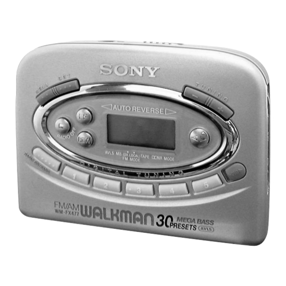
Photo: WM-FX477
Model Name Using Similar Mechanism
Tape Transport Mechanism Type
Notes on Chip Component Replacement
• Never reuse a disconnected chip component.
• Notice that the minus side of a tantalum capacitor may be dam-
aged by heat.
– 1 –
Canadian Model
AEP Model
Chinese Model
RADIO CASSETTE PLAYER
US Model
E Model
WM-FX483
MF-WMFX483-147
Advertisement
Table of Contents

Related Manuals for Sony WM-FX477


Summary of Contents for Sony WM-FX477
- Page 1 SERVICE MANUAL US Model Canadian Model Ver 1.0 1999. 02 AEP Model E Model Chinese Model Photo: WM-FX477 Dolby noise reduction manufactured under license from Dolby Labo- Model Name Using Similar Mechanism WM-FX483 ratories Licensing Corporation. Tape Transport Mechanism Type MF-WMFX483-147 “DOLBY”...
-
Page 2: Table Of Contents
TABLE OF CONTENTS 1. GENERAL ................3 2. DISASSEMBLY 2-1. Cabinet (Front) Assy ............5 2-2. Display Board ..............6 2-3. Holder (Sub) Assy, Cassette ..........6 2-4. Main Board ................. 7 2-5. Mechanism Deck ..............7 2-6. Belt and Motor ..............8 3. -
Page 3: General
SECTION 1 GENERAL This section is extracted from instruction manual. – 3 –... - Page 4 – 4 –...
-
Page 5: Disassembly
SECTION 2 DISASSEMBLY • The equipment can be removed using the following procedure. Cabinet (front) assy Display board Main board Mechanism deck Belt and Motor Holder (sub) assy, cassette Note : Follow the disassembly procedure in the numerical order given. 2-1. -
Page 6: Display Board
2-2. DISPLAY BOARD 1 screws 3 DISPLAY board 2 four claws 2-3. HOLDER (SUB) ASSY, CASSETTE 2 Insert a precision screwdriver (1.4 mm flat-blade) vertically into portion A to release the hinge plate. 3 Portion B to release the hinge plate. 5 spring (torsion) 1 Open the holder (sub) assy, cassette. -
Page 7: Main Board
2-4. MAIN BOARD Note : When installing, fit the switch and slider. 3 screw (M1.4x2.0), locking 2 Unsolder the 4 places. 6 MAIN board switch 5 three claws slider 4 three claws 1 HEAD FLEXIBLE board (CN303) 2-5. MECHANISM DECK 1 screw 4 Remove the mechanism deck in the direction of the arrow. -
Page 8: Belt And Motor
2-6. BELT AND MOTOR 2 two screws (screw (M1.4), special head) 3 motor • How to apply the belt belt M901 wheel assy (SP), capstan 1 belt – 8 –... -
Page 9: Mechanical Adjustments
SECTION 3 SECTION 4 MECHANICAL ADJUSTMENTS ELECTRICAL ADJUSTMENTS PRECAUTION PRECAUTION 1. Clean the following parts with a denatured-alcohol-moistened • Supplied voltage : 2.5V swab : • Control position playback head pinch lever assy VOL control : maximum capstan wheel assy rubber belt 2. -
Page 10: Tuner Section
TUNER SECTION 0 dB = 1 µV • AM Section Setting: • FM Section RADIO ON/BAND switch : AM Setting: RADIO ON/BAND switch : FM AM Tuning Voltage Adjustment FM Tuning Voltage Adjustment digital voltmeter digital Main board voltmeter TP (VT) Main board TP (VT) AM TUNING VOLTAGE ADJUSTMENT... - Page 11 Adjustment Location: main board – main board (side A) – AM TUNING VOLTAGE ADJUSTMENT FM TUNING VOLTAGE ADJUSTMENT AM TRACKING ADJUSTMENT FM TRACKING ADJUSTMENT AM IF ADJUSTMENT Measurement Points: main board – main board (side B) – (VT) FM RF IN (FM RF IN) –...
-
Page 12: Diagrams
VER3 Destination select input (Fixed at “L” in this set.) MBSET MEGA BASS with/without detection input (Fixed at “L” in this set.) DOLBY with/without detection input (Fixed at “L” (WM-FX477) or DLBSET “H” (WM-FX479) in this set.) REV SW Mechanism deck mode detection switch input (REV ON: H) -
Page 13: Block Diagram
WM-FX477/FX479 Pin No. Pin Name Pin Description 5-2. BLOCK DIAGRAM — Stabilized capacitor connection of crystal oscillation power supply. VLCD — LCD driver power rising pressure pin AUDIO 78, 79 C1, 2 — LCD driver power rising pressure pin POWER AMP IC301(1/2) —... -
Page 14: Schematic Diagram -Main Section
WM-FX477/FX479 5-3. SCHEMATIC DIAGRAM — MAIN SECTION — • Refer to page 25 for IC Block Diagrams. (Page 23) Note: • All capacitors are in µF unless otherwise noted. pF: µµF 50 WV or less are not indicated except for electrolytics and tantalums. -
Page 15: Printed Wiring Board -Main Section
WM-FX477/FX479 5-4. PRINTED WIRING BOARD — MAIN SECTION — • Semiconductor M901 CAPSTAN/REEL Location MOTOR Ref. No. Location G-10 D401 D402 D731 H-10 IC301 D-11 <IC331> PH701 (Q2) H-10 Q101 F-11 Q201 F-11 Q301 Q302 D-12 Q303 F-12 Q304 Q305 HP901 <Q331>... -
Page 16: Printed Wiring Board -Display Section
WM-FX477/FX479 5-5. PRINTED WIRING BOARD — DISPLAY SECTION — • Semiconductor Location Ref. No. Location IC701 IC702 B-12 Q701 Q702 Q703 C&SA (Page 19) PANEL Note: • : Through hole. ® • Abbreviation • b : Pattern from the side which enables seeing. -
Page 17: Schematic Diagram -Display Section
WM-FX477/FX479 5-6. SCHEMATIC DIAGRAM — DISPLAY SECTION — (Page 18) Note: • All capacitors are in µF unless otherwise noted. pF: µµF 50 WV or less are not indicated except for electrolytics and tantalums. • C : panel designation. • U : B+ Line. -
Page 18: Exploded Views
SECTION 6 EXPLODED VIEWS NOTE: • IC Block Diagrams • The mechanical parts with no reference • Color Indication of Appearance Parts • Abbreviation number in the exploded views are not supplied. Example : CND : Canadian model. IC1 TA2104 •... - Page 19 Ref. No. Part No. Description Remark Ref. No. Part No. Description Remark 3-349-825-31 SCREW 3-892-535-11 SCREW 3-019-422-01 JOINT 3-030-025-01 HOLDER (LCD) 3-022-857-01 SPRING (OPEN) 3-030-018-01 BUTTON (PRESET) 3-019-421-01 LEVER, OPEN X-3376-953-1 CABINET (FRONT) ASSY (DX/LOCAL) (SILVER) 3-022-856-01 SPRING (KNOB), TENSION (FX479:US,CND,C&SA) X-3376-954-1 CABINET (FRONT) ASSY (ST/MONO) (SILVER) 3-020-512-01 TERMINAL (-), BATTERY...
-
Page 20: Tape Mechanism Deck Section
6-2. TAPE MECHANISM DECK SECTION (MF-WMFX483-147) HP901 M901 Ref. No. Part No. Description Remark Ref. No. Part No. Description Remark X-3375-020-1 PINCH LEVER (N-F) ASSY 3-703-816-31 SCREW (M1.4), SPECIAL HEAD X-3369-747-1 WHEEL ASSY (SP), CAPSTAN X-3375-021-1 PINCH LEVER (R-F) ASSY 3-354-868-01 BELT 3-703-816-73 SCREW (M1.4), SPECIAL HEAD 3-021-950-01 GEAR (DF) -
Page 21: Electrical Parts List
SECTION 7 DISPLAY ELECTRICAL PARTS LIST NOTE: • Due to standardization, replacements in • Items marked “*” are not stocked since When indicating parts by reference the parts list may be different from the they are seldom required for routine service. number, please include the board. - Page 22 DISPLAY MAIN Ref. No. Part No. Description Remark Ref. No. Part No. Description Remark < SWITCH > 1-165-176-11 CERAMIC CHIP 0.047uF 1-109-935-11 TANTAL. CHIP 4.7uF S701 1-572-922-11 SWITCH, SLIDE (HOLD) 1-124-434-00 ELECT 220uF 1-162-974-11 CERAMIC CHIP 0.01uF < VIBRATOR > 1-115-467-11 CERAMIC CHIP 0.22uF X701...
- Page 23 MAIN Ref. No. Part No. Description Remark Ref. No. Part No. Description Remark C313 1-162-927-11 CERAMIC CHIP 100PF < FILTER > C331 1-135-201-11 TANTALUM CHIP 10uF (FX479) 1-236-711-21 FILTER, BAND PASS (EXCEPT EE) C334 1-135-201-11 TANTALUM CHIP 10uF 1-239-813-21 FILTER, BAND PASS (EE) (FX479) C335 1-162-964-11 CERAMIC CHIP...
- Page 24 MAIN Ref. No. Part No. Description Remark Ref. No. Part No. Description Remark Q605 8-729-141-48 TRANSISTOR 2SB624-BV345 R107 1-216-864-11 METAL CHIP 1/16W Q606 8-729-141-48 TRANSISTOR 2SB624-BV345 (US,CND) Q607 8-729-421-26 TRANSISTOR UN5216 R108 1-216-811-11 METAL CHIP 1/16W Q751 8-729-421-26 TRANSISTOR UN5216 (EXCEPT US,CND,FR) Q752 8-729-420-24 TRANSISTOR 2SB1218A-QRS...
- Page 25 MAIN Ref. No. Part No. Description Remark Ref. No. Part No. Description Remark R603 1-216-845-11 METAL CHIP 100K 1/16W MISCELLANEOUS R604 1-216-845-11 METAL CHIP 100K 1/16W *************** R605 1-216-833-11 RES,CHIP 1/16W R606 1-216-845-11 METAL CHIP 100K 1/16W HP901 1-500-555-11 HEAD, MAGNETIC (PLAYBACK) R607 1-216-845-11 METAL CHIP 100K...
- Page 26 WM-FX477/FX479 Sony Corporation 99B0482-1 Printed in Japan C1999. 2 9-926-959-11 Personal A&V Products Company Published by Quality Engineering Dept. – 34 – (Shinagawa)