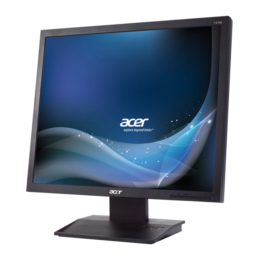
Acer V173 Service Manual
Lcd monitor
Hide thumbs
Also See for V173:
- Service manual (82 pages) ,
- User manual (28 pages) ,
- Quick start manual (3 pages)
Table of Contents
Advertisement
Advertisement
Table of Contents

Related Manuals for Acer V173


Summary of Contents for Acer V173
-
Page 1: Service Manual
Service Manual LCD Monitor Acer V173 - 0 -... -
Page 2: Table Of Contents
Copyright 2008 Acer Incorprated All Rights Reserved This manual may not, in whole or in part, be copied, Photocopied, reproduced, translated, or converted to any electronic or machine readable form without prior written permission of Acer Incorporated. Acer V173 Service Manual... -
Page 3: Important Safety Notice
Important Safety Notice Safety precautions This monitor is manufactured and tested on a ground principle that a user’s safety comes first. However, improper used or installation may cause damage to the monitor as well as to the user. Warning: This monitor should be operated only at the correct power sources indicated on the label on the rear of the monitor. -
Page 4: Product Specification
01 Product Specification General: ACER BV173 is designed with LVDS interface and dual (VGA&DVI) input, it featured with embedded universal AC power supplies. It’s a green product and meets all ROHS standard. The power button and display control buttons are on the front of the monitor. The monitors shall automatically display lower resolution video modes into 1280x1024 full screen display .The image can be adjusted through OSD control. -
Page 5: Electrostatic Discharge Requirements
Storage -20°C to 60°C Temperature range Relative humidity 5% to 80% Altitude 0 to 9144M (30000 ft) 2.2 Safety, EMC, Ergonomics and Compatibility Requirements Items Description TUV/ Other Safety ● ● ● ● ● ● ● ● ● Ergonomics ● ●... - Page 6 +5V output <150mv DC Output Voltage and Current 13.5V-15.6V 1.4A(typ.),1.8A(max) 4.9V-5.3V 1.1A(typ.),1.4A(max) Power consumption without Audio ≤35W Protection See Table-1 Power management See Table-2 Notes: 1. Before each test, the buck capacitor need to be discharged. 2. Before each test, it must be 10 minutes at least after the latest test. Table-1 Protection Condition...
-
Page 7: White Balance Adjustment
Frequency 40.0 @Brightness=3.3V Output Current for mArms INL MT170EN01_VC One Lamp Operating Voltage Vrms INL MT170EN01_VC Kick Off Voltage @Vin=13.5V Hold Up Time Brightness=3.3V 3.3 Brightness output The test to verify specifications in this section shall be performed under the following standard conditions unless otherwise noted. - Page 8 Input / Output Signal Specifications 4.1 Signal Interface Items Condition Spec Note ● Color: Gray 15 pin D-Sub Signal Cable Length: 1800 20 mm Signal type Separate analog R,G,B ● For 15 pin D-sub 700 mV +/- 5% (peak to ●...
-
Page 9: Function Specifications
EDID Data Table : See the attached table (for example) EDID Table For InnoLux MT170EN01_VC Pane 4.1.1 V173 VGA EDID table (INL VC 17’ Panel) 4.1.2 V173 DVI EDID table (INL VC 17’ Panel) Function Specifications 5.1 Panel General Specifications All the tests to verify specifications in this section shall be performed under the following standard conditions unless otherwise noted. - Page 10 “ACER e Color Management” and “User” to instead “Contrast” and “Brightness” separately. When press “ACER e Color Management” to show “e Color OSD”, and press “User” to show OSD interface before. The translations of “ACER e [MENU] Color Management” and “User” are always English.
- Page 11 The On-Screen Display (OSD) shall be an easy to use icon based menu through keypad OSD buttons or remote control unit. The unit shall leave the factory with all OSD controls set to their default values. First Second Third Control Range Default Value ACER e COLOR Empowering Management Technology User mode Text mode Contrast...
- Page 12 Suomalain Hor. Position 0 ~ 100 Ver. Position 0 ~ 100 OSD Timeout 10~ 120 Analog Input (Dual) Digital DDCCI ON/OFF Input (Analg DDCCI ON/OFF only) Resolution H. Freq Info V. Freq ETL000….0000(22) Reset Exit Notes: 1. Clock default 50 is for Visa timing. Others depend on timing. 5.3.1 OSD Function Test 3.1.1 Test mode: 1280x1024 @ 60 Hz 3.1.2 Test pattern: pattern #1 of crosshatch (GENERAL-1)
-
Page 13: Display Check
Standby (No H/V sync) < 1W Orange Power off < 1W No display 5.7 VGA Cable Detect Test If VGA cable of LCD monitor isn’t connected to video pattern generator or PC, “NO SIGNAL” should be shown on screen. Hi-Pot test Test condition: a. - Page 14 Distance between Bright dots L ≥ 15 mm ● Distance between Dark dots L ≥ 15 mm ● Note 1: Dot defect is defined as the defective area is not larger than 50% of the dot area. Bright Dot is defined 5% transmission ND filter.
- Page 15 Equipment: PC, ISP card, signal cable and power cable. ESD requirements: antistatic wrists, antistatic gloves (fingers), and connecting cable Name of ISP program: RTDTool_4.6.exe Manufacture of FW IC RTD 2525L Operational steps: 1. Connection: connect PC to PCBA with signal cable, and then keep AC and DC in open state 2.
- Page 16 Select Bank2 size: 30 Thirdly, click “64K”button and download FW file as below Figure 3.
- Page 17 Fourthly, click “64~96”button, and download extern FW file as below Figure 4 . Fifthly, click“program”button as below, then you will see ISP will going on. There will be prompting if programming is OK.
- Page 18 Program button Note: Please see the configure as below Figure 6. Configure Inform Programming speed...
-
Page 19: Factory Mode
After connecting, AC ON, DC ON Flowing chart Open ISP program Choose manufacturer and model of FW IC LOAD FW files Click program button Beginning Choose Config and adjust programming programming Turn off power if programming is OK 7.3 Factory Mode HOT KEY OPERATION FUNCTION AUTO... -
Page 20: Flat Panel Specification
02. Flat Panel Specification... -
Page 37: Exploded Diagram
03 Exploded Diagram 3.1. LCD Exploded drawing (All) - Page 38 3.2 Assy Bezel Exploded drawing...
- Page 39 3.3Assy BACK COVER Exploded drawing For VC panel...
- Page 40 3.4 Assy BACK COVER Exploded drawing for AUO panel...
-
Page 41: Troubleshooting
Troubleshooting 1. Common Acknowledge 1.1 Monitor Block Diagram The LCD Monitor contains an interface board, and inverter/power keypad board and flat panel. In Inverter/power/Audio board, power section supplies +14V & +5V for Inverter and Interface board used. The inverter section drives the backlight of panel and the DC-DC conversion. Flat panel (LVDS interface) and CCFL Inverter/Power Interface Board... - Page 42 which composed of 4 build-in diodes, it inverts AC to DC. 1.3.1.2 High Voltage to Low Voltage Control Circuit C804 is used to smooth the wave from rectifier. IC802 is a highly integrated PWM controller. When rectified DC high voltage is applied to the Vcc pin during start-up, the MOSFET Q804 is initially off, and the Vcc pin capacitor is charged.
-
Page 43: Inverter Circuit
#14,#22,#10,#21 through R141,R138,R135,R140,via CN901 #5, #6, #8, #7. - LED Indicator on Front Bezel 1 When press button “power”, U102 (MCU) #1 sends out a low potential, via R130, flow to CN901 #2 on keypad, LED Blue ON. 2 When in “Suspend” mode, U102 (MCU) #48 sends out a low potential, via R129, flows to CN901 #4 on keypad, LED Amber ON. - Page 44 No Power & Power LED Off No power Check IC802, Check circuit Check primary C804, T801 if short rectifier voltage Check F801, P801, D801 Check pin7 of Check R806, R807, IC802 voltage R808, about 13V Check R808, R819, Check pin8 of IC802 voltage about 2.5V Check IC801 and Check pin2 of IC802...
- Page 45 2. DC output voltage is unstable Output voltage unstable Check ZD801, D803, Check circuit Check Vbe of D805 if short Q801below 0.3V Check Q801,Q802 Check R832,, IC801, Check Pin R of Check reference IC803 voltage voltage about 2.5V Check R822, R823 Check R815, c814, Check feedback Check vpin2-4of...
- Page 46 4. No Raster No raster? LED Blue? Backlight can’t be turned on. Is there 14Vdc Check power voltage on pin9 supply of IC501? Is there high-level Is Ok R510? voltage on pin8 of Check I/F IC501? board R501 open Connecting the Are connected rightly output connector CN501, CN502,...
- Page 47 5. Black Screen...
- Page 48 6. Bad Screen...
- Page 49 White Screen...
-
Page 50: Spare Parts List
Spare parts List 8171J061A020R 8171J071A020R OEM PART NO DESCRIPTION 791421300600R PCBA,I/F BOARD(VC,EMEA),LE17J0-610 ROHS 791401500000R PCBA,KEYPAD BOARD,LE9D0-612 ROHS 791421400600R PCBA,P/I BOARD,W/O SPK,LE17J0-622 ROHS 791421300700R PCBA,I/F BOARD(EMEA,W/O),LE17J0-710 ROHS 430300801670R HRN ASSY 2x4P 55mm UL1571#28,ROHS 430300801760R HRN ASSY 2x4P to 8P 160mm UL1571#28,ROHS 430303001520R HRN LVDS FFC 30P 231mm W/MYLAR&Core ROHS 453070800210R... -
Page 51: Schematics And Layouts
06 Schematics and Layouts 5DVCC 3.3VCC U101 LD1117AL-3.3V 5DVCC CN101 VIN VOUT C141 Shoule be canceled for the brightness is not so good BKLT-EN VBRI 2 VOLUMN 2 MUTE 2 8P 2.0mm 5DVCC VLCD 3.3VCC Q101 AP2305GN R103 BKLT-EN R104 Q102 2N7002 INVON 2... - Page 52 MCU_VCC D101 D102 SN4148 SN4148 MCU_VCC MCU_VCC MCU_VCC 3.3VCC DSUB_5V Q105 PMBT3906 R107 3.3VCC C112 C111 10u/25V 0.1/16V Q106 PMBT3906 PANELPOWER_ON/OFF 1 RTD_SD3/SDI 4 MCU_RESET RTD_SCLK 4 R128 VBRI P5.0/PWM0 VOLUMN P5.1/PWM1 INVON P5.2/PWM2 MUTE P5.3/PWM3 LED2 R129 P5.4/PWM4 LED1 R130 P5.5/PWM5 DSCL/P5.6...
- Page 53 DSUB_5V CN103 DSUB_5V 2 DZ11AA1-H5W6-4F FB101 60Ω R149 C117 0.047u/16V RTD_R+ 4 R150 C118 0.047u/16V RTD_R- 4 FB102 60Ω R151 C119 0.047u/16V RTD_G+ 4 R152 C120 0.047u/16V RTD_G- 4 FB103 60Ω R153 C121 0.047u/16V RTD_B+ 4 R154 C122 0.047u/16V RTD_B- 4 3.3VCC R155 R156...
- Page 54 3.3VCC TMDS_VDD FB105 60Ω C131 3.3VCC 0.1/16V C132 0.1/16V R144 R132 R1.8DVCC R1.8DVCC Q110 PMBT2907A C134 C133 C135 C136 C137 0.1/16V 0.1/16V 0.1/16V 0.1/16V 10u/25V CN104 FFC-CON Q111 PMBT2907A RXO0- RXO0- RXO0+ RXO0+ RXO1- RXO1- RXO1+ RXO1+ RXO2- RXO2- RXO2+ RXO2+ TMDS_VDD U104...
- Page 55 R827 C815 1000p/500V C805 T801 2200p/400V SPW-0xx DC 380V Max. SR5150PT R805 D803 L802 0R2 1W +14V R834 R835 R804 R831 D801 68K 2W 100Ω 1W C804 ZD801 BL4-06 C817 82u/450V C806 R828 C816 C819 1000p/500V 4700p/400V 1000u/25V 470u/25V Q801 D802 R830 2PC1815GR...
-
Page 57: Assembly And Disassembly
7.0 Assembly and Disassembly (1).Take panel out of box and place it on the foam. (2).Tear open the PE bag and put it in LCP 17" the designated carton. MT170EN01- Place (3).Place panel on the foam like the 631102072741R panel attached picture. - Page 58 Assembly and Disassembly continue) 1.Reverse the panel by 180 degree,put the surface of panel upsides and insert front bezel in the panel. 2.Reverse the panel by 180 degree using both hands,put the surface of panel downsides and make sure FFC interface is closer to operator.
- Page 59 Insert powerboard into the designated Fix chassis PCBA,P/I BOARD,W /O 791421401600R location of chassis ,like the attached &poweboard SPK,LE17K0-622 ROHS Picture HRN LVDS FFC 30P Connect Connent powerboard with the relevant 284mm mainboard&power PIN in the mainboard like the attached 430303001520R W/MYLAR&Core board...
- Page 60 Fix 3 pcs of screws separately on the poweboard and mainboard like the attached Picture1 Tear adhensive film out of adhensive film like attached Picture Paste FFC wire on the disignated location like the attached Picture...
- Page 61 (1). Handle hexagonal screws and electric opener (2). Twist screw in the interface like the attached Picture1. (3). Place cushion on the designated location after iron frame is taken away. Thread lamp wire into the relevant hole of chassis like the attached Picture 1.Tear off the adhensive tape of FFC wire;...
- Page 62 Check if back cover is fixed properly Fix stand on the back of assemble like attached Picture Check if base is qualified and insert it into the relevant location properly like the attached Picture (1)Release monitor to the packing line (2)Put monitor into carton like the attached picture...